Semiconductors
1/166
There's no tags or description
Looks like no tags are added yet.
Name | Mastery | Learn | Test | Matching | Spaced | Call with Kai |
|---|
No analytics yet
Send a link to your students to track their progress
167 Terms
A Conductor is
a material through which electricity passes easily because it has free electrons
What material offers very little resistances to the flow of electrons?
Conductors
What 3 metals/conductors allow electricity to pass easily?
Silver copper and aluminum
Silver is a better conductor than ?
copper
Copper is used more frequently because ?
Because it is cheaper
Aluminum is used as?
Is used as a conductor where light weight is important
Why are some materials good conductors ?
One of the most important reasons is the presence of free electrons.
If a material has many electrons that are free to move away from their atoms , that material will be ?
That material will be a good conductor of electricity
Although free electrons usually move in a haphazard (lacking any obvious principle of organization) way , their movement can be ?
There movement can be controlled (electric current )
Electric current is a flow that control ?
electrons to move in the same direction
Conductors may be in the from of?
Bars , tubes, or sheets
The most familiar conductors are ?
Wire
To prevent conductors from touching at the wrong places they are usually coated with plastic, rubber , or cloth material called and ?
Insulator or insulation
various electrical applications require different ?
Different conductor sizes
Electrical wire -
is designed by definite gauge sizes that designate wire of a specific diameter.
As the diameter of wire decrease , The gauge number increase this is an example of
Inversely proportional
Copper wire is often stranded because stranded wire is ?
Stranded wire is easily bent without breaking
To bend or flex wire constantly , it is necessary to ?
To make many smaller strands into a cable or bundle. This allows for the flexing of the cable or wire without breaking
What is lamp cord made of ?
The lamp cord in your home is made of fine strands of copper wire. This allows it to be flexible and bend where you want it on the way from the plug to the lamp.
Larger wire used for wiring commercial or industrial buildings are ?
Are also stranded
Any number of small wire are grouped In a cable to carry ?
To carry the same amount of current a solid conductor wire
The larger wires have to be stranded because ?
Larger wires have to be stranded so they'll be easier to bend and work with if not it would be impossible to work with them
A solid No. 18 wire
is easily bent , but it's not as flexible as a multiple-strand cable
multiple-strand cable -
made up of smaller gage wire to equal the No.18 wire used in lamp
Insulator
a material with very few , if any, free electrons
No known material is a perfect insulator , however there at materials that are poor conductors that are classified as insulators such as,
Glass , dry wood , rubber, mica , and certain plastics
in between insulators and conductors are?
Semiconductors
semiconductors are
Materials that have conductivity properties about halfway between good conductors and good resistors
semiconductor materials are
the foundation of the vast array of electronic devices that surround us including
Computers, telephones, radios , televisions , refrigerators , microwave ovens , automobiles , airplanes, traffic lights , light-emitting diodes (LEDs)
Diode
a semiconductor device with terminals , typically allowing the flow of current in one direction only
The properties of semiconductor materials are
Silicon and germanium
Silicon and germanium are useful in electronic devices like
Integrated circuits , chips, transistors , diodes, & solar cells.
Semiconductor solar photovoltaic panels directly covert light energy into
Electrical energy
The electronic properties and conductivity of a pure or intrinsic semiconductor material can be changed in a controlled way to make them limited and predictable conductors by adding very small quantities of other elements such as
Boron or phosphorous to the melted semiconductor and then letting them melt to solidify back into a crystal form .
semiconductor is applied to both
Diodes and transistors as well as certain special types of electronic devices
germanium and silicon perform somewhere between the level of
Conductor and insulator in terms of opposition to current flow
The amount of opposition is programmed into it manufactured into the device by
Controlling the impurities introduced into pure germanium or pure silicon
Germanium and silicon can be purified to better than
99.999999 percent
By controlling the amount of doping agent introduced into each crystalline structure, manufactures can control
Can control the amount of opposition to current flow
Semiconductor diode is made by
Joining a piece of P material with a piece of N material
The place where two materials are joined is referred to as
the junction
The Junction is
Very thin , and each end had a piece if wire attached for connecting the diode , thus making a circuit
Both holes and electrons are involved in
Conduction in the PN junction diode
The holes in the N material near the junction are attracted by
Attracted by the negative ions on the P side of the junction and pass across the junction
Free electrons produced on the P side of the junction pass across the junction and
And neutralize positive ions on the N side ( example of intrinsic conduction)
Because of intrinsic conduction the junction is no longer
Is no longer a rectifier when an external voltage is applied across it
The point contact diode
is a very small unit that is used for rectifying signals.
Rectifying power
line frequencies and higher currents.
Unlike the junction diode , the point contact type depends on
Depends on the pressure or contact between a point and a semiconductor crystal for its operation
In a point contact diode
one section consists of a small , rectangular crystal of N material (either germanium or silicon) and a fine beryllium copper, phosphor-bronze , or tungsten wire called the cat whisker
Cat whiskers
presses against the semiconductor material and forms the other part of the diode
The reason for using a fine - pointed wire instead of a flag metal plate is to produce
Produce a high density electric file by the point of contact without using too large external voltage source.
The opposite end of the cat whiskers is used as
The diode terminal for connection purposes
Since the size of the cat whisker is limited , the amount of current the diode can handle is also limited
Tunnel Diodes
Tunnel diodes can be used in extremely small spaces , such as
part of an integrated circuit (IC) or chip.
Tunnel diodes can switch at
very high rates [ 2 to 10 gigahertz (GHz) ]
A gigahertz
is 1,000 megahertz (MHz)/ 1 billion times per second
Tunnel diodes are doped by using
Gallium arsenide, gallium antimonide, and indium antimonide
A megahertz is
1 million times per second
Silicon - controlled rectifier (SCR)
is a specialized rectifier or diode; is a specialized four-layer type of device used for the control of current on its cathode-to-anode path.
What is used to control the resistance between the cathode and anode?
a gate
An SCR conducts current in
In the forward direction only
Examples of SCR are
Light dimmer and the speed control for an electrically powered small hand drill
what is a feature of a conductor regarding their atomic structreq
less than 4 electrons in its valence band
this overlaps with the conduction band
what is a insulator
a material with no free electrons
What is a diffrence between conductors and a semi conductor
a semi conductors valence shell does not overlap with conductors
what is doping
adding very small amounts of a different element with either more, or less electrons in its outer shell.
what is the process of doping
an impurity is introduced into the semi conductor in order to change its electrical conductivity
it allows it to act like either a semi conductor or in insulator
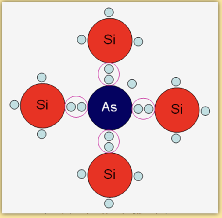
N type conductor what is it.
add a small number of atoms aresenic (As) with five outer electrons in its outer shell to pure silicon with four. we end up with a spare electron in the conductor layer.
because atom can have 8 in this band because its silicon and we bond them we would have an extra electron this process is what doping is
we do this because that free electron can now carry charge make it N(egative) type
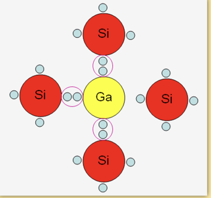
What is a P type semi conductor
now beacause silicon has four outer electrons if we add something like gallium with 3 outer electrons gives 7 not 8 outer electrons leaving a hole that can attract electrons
this creates electric current
P(ostive) type
what happens if we attach a piece of P type to a piece of N type
we get a “depletion layer” because its depleted of free charge carriers
what is a diode and its property
n type joined to p type doped semi conductor
its fundamental property is to conduct electric current in only one direction
how can we use the diode and how does it work
force current in one direction by reinforcing/eliminating the depletion layer can flow across the diode
what is a transistor
two diodes using three layers of semi conductor
what if we apply two different power supplies with enough voltafe to a two diodes
becomes transistor which functions as an electron switch
how can we use semi conductors to create a switch
we need three layers of them
what is a photodiode
a semi conductor that converts light into electrical current
the current is generated when photons are absorbed by the photodiode
the light energy creates a hole within the depletion layer which allows current to flow
at night what does the photodiode do
its semiconductor acts as an insulator and at day its a conductor
what is CCDs
2d rays of photodioded that chanhe light into a grid of electrical charge
all of the photodiode is a pixel. so more light on it means more charge created
what must we do to the charge in photodiode to make it useful
moved to main memory using a shift byte by byte
Semiconductor
Materials that conduct electricity at values between that of a pure metal and a good insulator.
Doping
The process of adding impurities to pure semiconductors to enhance their conductivity.
N-Type
Materials with negatively-charged carriers (free electrons) due to the presence of donor impurities, determining conductivity.
P-Type
Materials with positively-charged carriers ("holes") due to the presence of acceptor impurities, determining conductivity.
P-N junction diode
Formed by joining a P-Type semiconductor to an N-Type semiconductor, creating a single semiconductor-crystal structure.
Magnet
Any material or object that produces a magnetic field.
Magnetic Field
A volume of space where magnetic forces are exerted.
Law of Magnetism
Like poles repel, unlike poles attract.
Magnetization
The process where a magnetic material acquires magnetism, either temporarily or permanently.
Electromagnet
A current-carrying conductor wrapped around an iron core.
Magnetic Flux
The number of lines of force in a magnetic field (φ).
Magnetic Flux Density
The number of lines of force per unit area in a given magnetic field (B).
Neutral Point
The point between magnetic fields where magnetic flux density is 0.
Angle of DIP
The angle between Earth's magnetic flux and the horizontal.
Angle of DECLINATION
The angle between magnetic North and geographic North.
What is the relationship between temperature and carrier concentration in intrinsic semiconductors?
Carrier concentration increases with temperature due to more electron-hole pairs being generated.
What are majority and minority carriers in semiconductors?
Majority carriers are the most abundant type of charge carrier in a doped semiconductor (electrons in n-type, holes in p-type), while minority carriers are the least abundant.
Define the term "acceptor" in the context of semiconductors.
An acceptor is an impurity atom that increases the number of holes (p-type).
What happens to the conductivity of an intrinsic semiconductor as temperature increases?
The conductivity increases rapidly due to the generation of more electron-hole pairs.