flat panel detectors/ DR
1/15
There's no tags or description
Looks like no tags are added yet.
Name | Mastery | Learn | Test | Matching | Spaced |
|---|
No study sessions yet.
16 Terms
flat pannel detector
an array of pixel-sized detectors (DELs) thats very flat and thin
-contains capacitor and thin film translator (TFT) switch
DELs
measures xray absorption
array of pixels fastened to glass base/ substrate
dexels - once exposure is recieved and signal is collected

absorption materials in detector
photo conductors- absorbs xrays and emits electric charge, also converts light to electronic signal
scintillators- phosphors that absorb xrays and emit light
absorption material determines whther IR is _______ or _________ capture
direct, indirect
two types of flat pannels
Direct and indirect
direct capture
-TFT converts xray to digital signal
-single step system, xrays strike photoconductor and converts to signal which is then temporarilly stored in DEL capacitor, TFT switching gate releases signal to be read out
-signal is rad out through edges of array of DELS (DEL contains signal), signal is read out line by line, signal is apmlified and sent to ADC for processing
-active layer: amorphous selenium (a-Se) photoconductor
array of hardware pixels or DELs (data elements)
-signal from attenuated beam is collected within DEL
3 components to label:
semiconductor surface area (a-Se)
capacitor - stores charge
TFT switching gate - releases charge for readout
fill factor
the % of detectors elements area dedicated to xray absorption
-high fill factor equals: higher contrast resolution, higher spatial resolution
TFT readout
DEL charges are read out on a pixel by pixel and column by column basis
indirect capture
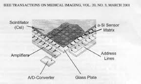
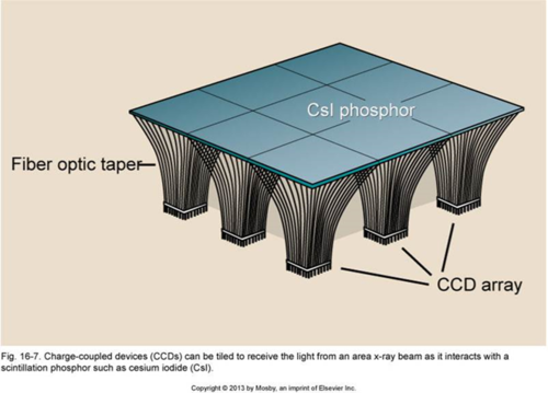
-scintillator and CCD (charge coupled device) or scintillator and TFT (thin film transistor)
-In CCD: light sensitive device that can respond to very low intensities, CsI is most common or GdOS, xray strikes scintilator and fiber optic cables collect light for read out, once recieved, applied charge is sent to ADC, uses A-Si
-TFT: xray strikes scintilator - CsI or GDOS and A-Si converts light to signal, TFT array captures charge in DEL and stores in capactor, TFT switch sends to ADC
-active layer - smorphous silicon (a-Si) photoconductor
scintillator: materila that absorbs xray and emits light

bucket brigade readout
-each DEL contains 3 electrodes that hold electrons in a potential well
-once bucket is full, can dump into amplifier at the end

DEL of indirect conversion system
-cesium iodide phosphor (top layer) absorbs xray and emits light, entire array of DELS covered with screen of cesium iodide
-amorphous silicon then absorbs light and emits electrons
unstructured vs structured scintillaotr construction
un:
-light scatters, reduced spatial resolution
Structured:
-needle like structure, increased interactions, less light speed, improved resolution
CMOS (complimentary metal oxide conductor)
indirect capture type
always compared to CCD array
scintillator works the same, each DEL contains its own transistor, amplifier, noise correction circuit and digitization circuit which results in lower fill factor and higher noise
signal readout is slightly different from CCD, DELs charge is sent across the chip and read in a corner of the array
signal sent to ADC
CCD vs CMOS
CCD
better light sensitivity
greater fill factor for better quality
modular construction (easy for repairs)
uses more power (110x)
CMOS
more susceptible to noise
lower light sensitivity
lower fill factor
less power
inexpensive to manufacture
lower quality and lower resolution
DR artifacts
IMG lag (ghosting)- detector doesnt clear signal from previous image
Back scatter- non-appropriate collimation
Gain calibration- used to compensate for sensitivity variation across the detector