physics - electronics
1/51
There's no tags or description
Looks like no tags are added yet.
Name | Mastery | Learn | Test | Matching | Spaced |
|---|
No study sessions yet.
52 Terms
examples for electronic devices
Moblie phone , computers , televisions and radios
electrical conductors
Materials that conduct electricity
examples for conductors
copper, aluminum , iron , lead
mixed conductors
simultaneously conducting both electricity and ions
examples for mixed conductors
brass, nichrome , manganin
electrical insulators
Materials that do not conduct electricity
examples for insulators
ebonite , polythene , plastic , dry wood, asbestos, glass
The reasons for the conductors to have the ability to conduct electricity
the ability of some of the electrons in the atoms of such materials to move freely within the conductor
Electrons in the outer shells of conductors act in this manner
reason:
because they are not tightly bound to the nucleus
reason for insulators not having the ability to conduct electricity
There are very few electrons that are free to move
reason :
because inter-atomic bonds (covalent bonds) between the atoms of insulators are strong
semi conductors
Materials that conduct a small amount of electricity
examples for semi conductors
Silicon , germanium
( in crystalline form )
element symbol of silicon and germanium
Si , Ge
Silicon , germanium ( semiconductors ) group in periodic table
fourth
the number of electrons in the outermost shell of Silicon, germanium ( semiconductors )
four
the structure formed by Silicon , germanium ( semiconductors ) and it’s process
structure : crystal lattice structures
process:
by sharing the four electrons in their outermost shell to make covalent bonds with four nearby atoms
and thereby obtaining a stable electronic configuration
having eight electrons in the outermost shell.
the nature of bonds formed by Silicon , germanium ( semiconductors )
these bonds are
rather weak
can be broken from the thermal energy that is available even at room temperature, causing the release in electrons
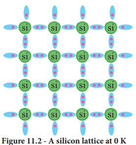
this fig described
shows the covalent bonds of the silicon lattice at 0 K.
All the bonds are complete at this temperature.
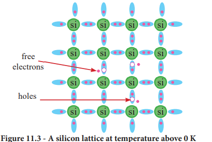
this fig described
shows that some bonds have been broken releasing some free electrons at a temperature higher than 0 K.
where can an electron deficiency can be observed
at the positions where the free electrons used to be
What is observed at the spots where the free electrons used to be?
An electron deficiency.
Why is there an electron deficiency at certain spots?
Because the free electrons have moved away from where they used to be.
positions with an electron deficiency known as
holes
Why does a hole in a solid act like a positive charge?
Because the missing electron means the positive protons in the nucleus are not neutralized.
In a neutral atom, what is the relation between protons and electrons?
The number of protons equals the number of electrons.
What is a “hole” in semiconductor physics?
A hole is the absence of an electron, which behaves like a positive charge.
Why is a hole in a semiconductor considered a positive charge?
Because when an electron is missing, the positive protons in the nucleus are not neutralized. In a neutral atom, protons = electrons, so the absence of an electron makes the hole act like a positive charge.
Missing electron → proton not neutralized → hole behaves positive.
In semiconductors,
not only electrons contribute to the conduction of electricity.
When an electron in an adjacent atom jumps to an atom with a hole having a positive charge,
the position of the hole can change.
By changing the position of a hole from one atom to another in this manner, holes can move around in the lattice and contribute in conducting a current.
charges of electrons and holes
Electrons - negative charge carriers
holes - positive charge carriers.
what happens when an electric potential difference is applied across a semiconductor ?
holes - move from the positive to the negative potential
electrons - move from the negative to the positive potential
the (conventional) current flows - from the positive to the negative potential.
the charge carriers that conduct electricity in metallic conductors
negatively charged electrons
In semiconductors
the negatively charged electrons as well as the positively charged holes act as the charge carriers that contribute in the conduction of electricity.
what is a hole generated for
in the breaking of a bond to release an electron
the number of carrier electrons present in a semiconductor is equal to the number of holes.
semiconductor lattice
is electrically neutral
reason for semiconductor lattice to be neutral
A semiconductor lattice is electrically neutral because the number of carrier electrons present is equal to the number of holes generated when bonds break, maintaining an overall balance of charges
intrinsic semiconductors
Pure semiconductor materials that exist in crystalline form
examples for intrinsic semi conductors
silicon (Si) and germanium (Ge)
Effect of Temperature on the Conduction of Electricity
Since,
the random motion of free electrons increases as the temperature is increased,
a rise in the temperature inhibits the current flow.
Therefore, a temperature rise in conductors causes a decrease in the conductivity (increase in the resistivity).
However in semiconductors, a rise in temperature breaks bonds generating more holes and free electrons
causing an increase in the conductivity (decrease in the resistivity).
extrinsic semiconductors
Carriers of the semiconductors that have been increased by doping it with another element
what happens when a minute amount of element phosphorus is mixed to a silicon ( intrinsic semiconductor)
Phosphorous is
an element in group V of the periodic table
has five electrons in the outermost shell.
A phosphorous atom
makes the number of electrons in its outermost shell eight by obtaining four electrons from four nearby silicon atoms around it.
In the process, one of the five electrons is left behind without taking part in forming a bond. This electron has the opportunity to move about freely in the lattice.( free electron)

what does this picture show ?
shows how a phosphorous atom forms bonds with silicon atoms
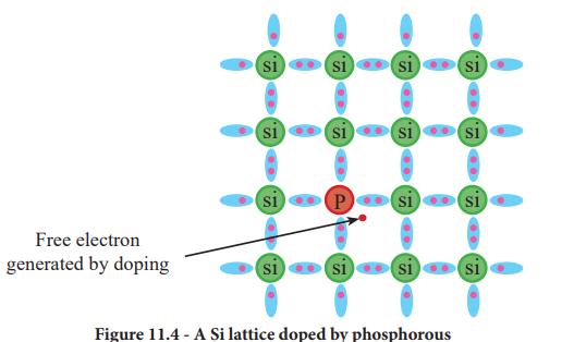
explain the fig
The electron left behind increases the conductivity of the lattice.
Since negatively charged electrons are introduced to the lattice as charge carriers, the semiconductor is known as a negative type or n-type semiconductor.
another way to form n-type extrinsic
By doping an intrinsic semiconductor with other elements in group V such as arsenic (As) and antimony (Sb)
what are donor atoms ?
electrons that are donated to the lattice by group V elements
what happens if a intrinsic semiconductor is doped with an element in group III
intrinsic semiconductor: silicon
element in group III : Boron
The boron atom forms bonds with nearby silicon atoms. However, since there are only three electrons in the outermost shell of the boron atom, there is a deficiency of one electron in order to form four bonds.
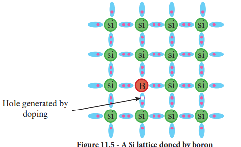
what does it show ?
shows how the atoms and bonds are configured in this case
Where does a hole exist in a boron-doped silicon atom?
At the point where the electron is deficient to form a bond
Why does the conductivity of silicon increase when holes are present?
Because holes can conduct electricity as positive charges.
Why are extrinsic semiconductors with holes called p-type?
Because a hole is equivalent to a positive charge.
In p-type semiconductors, which carriers are majority and which are minority?
Holes are the majority carriers, and electrons are the minority carriers.
How can p-type semiconductors be formed other than with boron?
By doping silicon with other group III elements such as aluminium (Al), gallium (Ga), or indium (In).
Why are group III elements called acceptor atoms in semiconductors?
Because they produce holes that can receive electrons.
What are accepter atoms ?