All things graphs
1/62
There's no tags or description
Looks like no tags are added yet.
Name | Mastery | Learn | Test | Matching | Spaced | Call with Kai |
|---|
No analytics yet
Send a link to your students to track their progress
63 Terms
How do you calculate dynamic resistance from and IV graph
Calculate the gradient by using a tangent - ohms law
Where is the operating point
A specified point on the graph
What are the IV characteristics for an ideal diode in forward bias
No voltage drop and current flowing
What are the IV characteristics for an ideal diode in reverse bias
No current flowing but a voltage drop
What are the V characteristics for a practical diode in forward bias
Voltage increases untill biasing voltage and then stops increasing.
What are the V characteristics for a practical diode in reverse bias
The increasing voltage is all dropped over the diode
What are the I characteristics in an practical diode in forward bias
No current flow until biasing voltage is reached and then maximum current flow
What is the I characteristics of an practical diode in reverse bias
No current flow
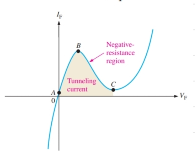
What happens to a tunnel diode in forward bias between A and B
The diode will start conducting after a very small amount of voltage and the current increases

What happens to a tunnel diode in forward bias between B and C
It shows negative resistance, and a potential barrier will start to form again

What happens to a tunnel diode in forward bias after point C
It begins to act as a normal diode again
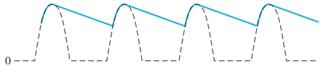
What would the time period of the wave give
The time period of the waveform at the output of the diode
Where is best to operated a Zener diode (graphical)
The knee

What does this graph show
The relationship between Vce and Ic for different Ib

What is the condition for the cut of region
Ib = 0

Why must IB = 0 to be in cut of region
As the base will not be conducting as it is either in reverse bias or not forward bias enough to conduct

If ideally there is no base current in cut off region, what is the actual approximation
A small amount of leakage current
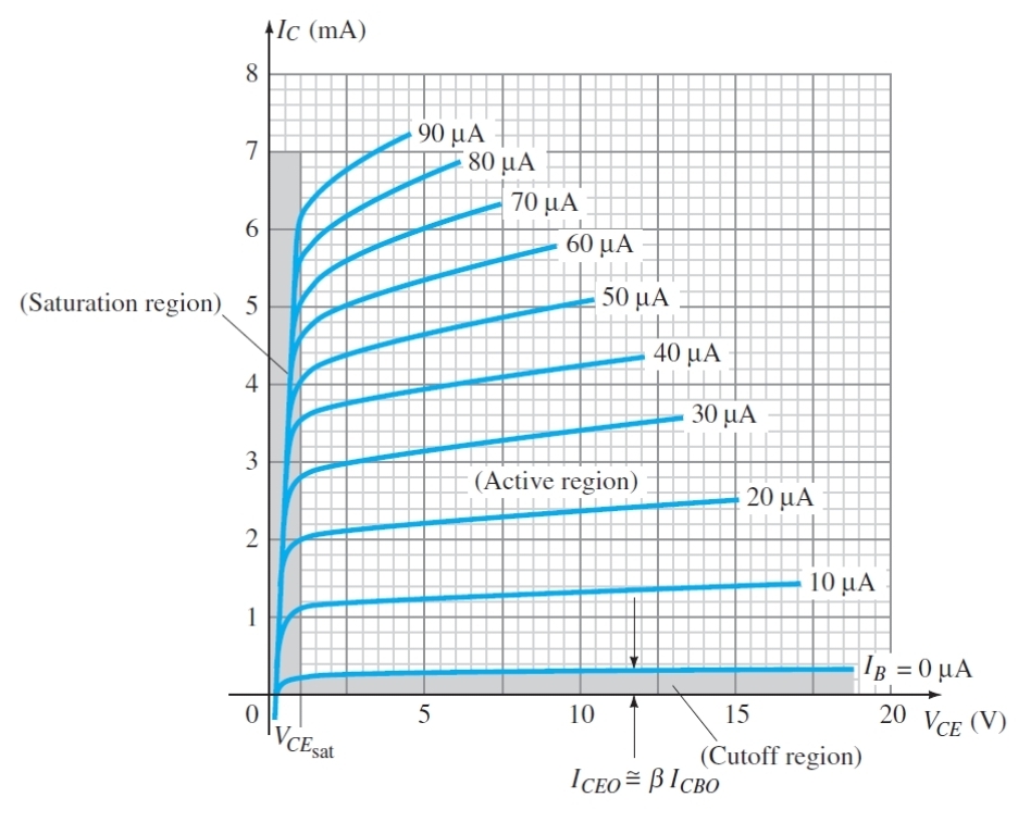
What is the condition to be in active region (Transistor)
Vce is high enough that is more positive than base and emitter

What is the condition for saturation region
Vce is low so both junctions are forward bias

Why does IB not significantly increase Ic in the saturation region
As the collector is saturated so its ability to take more current is limited by its voltage not Ib

What does the almost flat lines in the active region show for the relationship between IC and VCE
Vce does not effect Ic in this region

Why is the saturation region shaped like that
As both junctions are forward bias, charges flood the base quickly

What does VCEsat stand for (BJTs)
The collector - emitter saturation voltage

What is VCEsat (BJT)
The max value at which the transistor is still in the saturation region
What do you need to sketch a collector curve (BJTs)
Ic, Ib and Vce
What is a load line (BJT)
A straight line used to explain the behavior of the BJT in the 3 modes
What does a load line represent (BJTs)
The voltage and current in the linear portion of the circuit
What are the points called where the load line intercepts with the curves
Q points
What is a Q point
The optimal operation in the active region for that value of Ib
What two points do you need to draw a load line
Vce=Vcc and Ic = Icsat
What are FETs controlled by
Voltage
What does FET stand for
Field effect transistors
Which is more temperature stable, FETs or BJTs
FETs
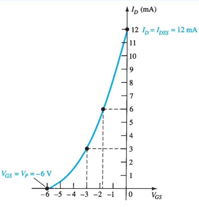
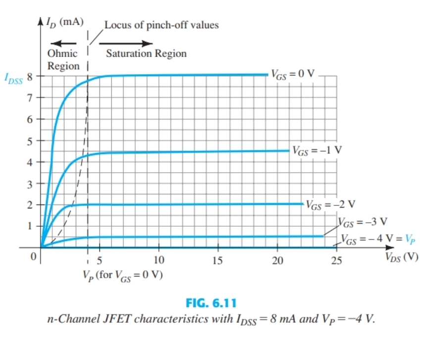
What is on the x-axis of a drain characteristic graph (JFET)
Vds
What is on the Y axis of a drain characteristic graph (JFET)
Id
At what point on a drain characteristic graph (JFET) does ID flatten off
Idss
On a drain characteristic graph (JFET) what is the value of VGS for IDSS
0
What happens to the line on the drain characteristic graph (JFET) when VGS is less than zero (-1, -2)
It looks the same but the current levels off at a lower value
What is this graph called
Transfer characteristic curve
What is plotted on a transfer characteristic curve (JFETs)
Id Vs Vgs
What is on the X axis of a transfer characteristic curve (JFETs)
Vgs
What is the max ID value for a transfer characteristic curve (JFETs)
Idss
What is on the Y axis of a transfer characteristic curve (JFETs)
Id
What is the min value for VGS for a transfer characteristic curve
Vp
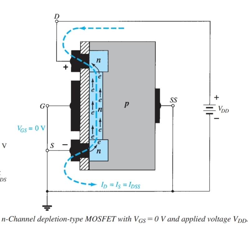
What are the IV characteristics for a MOSFET with Vgs = 0 the same as
JFET
Why does ID level off for the MOSFET
As a depletion region is caused by an electric field attracting the electrons out of the channel leaving very few charge carriers
What is the output of a comparator is the non inverting terminal is higher than the inverting
High signal
What is the output of a comparator where the input at the non inverting terminal is less than the inverting terminal
Low signal
What does the comparators output vary between
Two constant outputs with different polarities

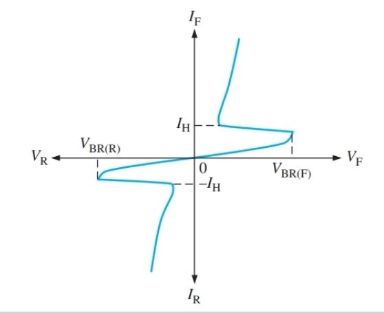
Why does the voltage decrease after going over VBR
When the device goes into saturation mode, voltage drops to very small but in active region there would be a voltage drop across the collector emitter junction

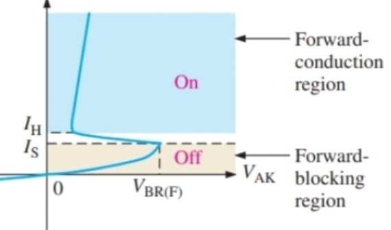
What is this graph
The IV characteristics of a thyristor

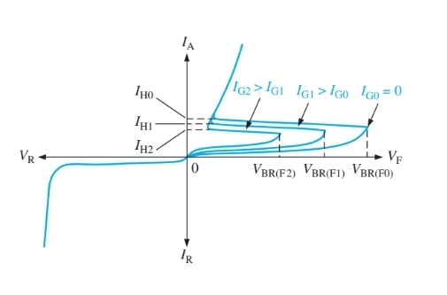
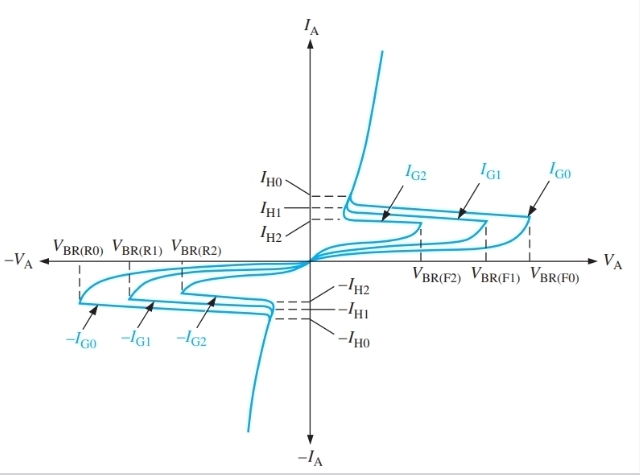
What will happen to VBR when a pulse is applied
It will decrease

What does the impact of IG tell us about VBR
A lower external potential will be required if there is a positive impulse on the gain terminal

What happens to VBR as IG increases
It decreases

How can current be decreased below IH
Decreasing the applied potential or having a circuit in place to do it

What values does Ig not effect
Switchover and holding values

If a SCR does not work for both directions of voltage, what does work
DIAC and TRIAC
What is a DIAC
A 4 layer device that can conduct with both polarities of applied potential
What is this the IV graph for
Shockley diode
What is this IV graph for
SCR
What is this IV graph for
DIAC
When is VBR at its max in a TRIAC
When Ig = 0
What is this graph for
TRAIC