Computer Systems Final Exam
1/30
There's no tags or description
Looks like no tags are added yet.
Name | Mastery | Learn | Test | Matching | Spaced | Call with Kai |
|---|
No analytics yet
Send a link to your students to track their progress
31 Terms
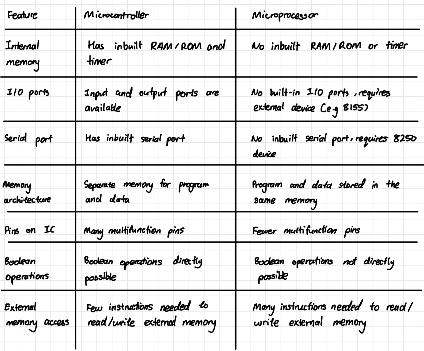
MCU vs MPU
Types of ISAs
RISC (Reduced Instruction Set Computer): Use a small, simple. and highly optimised set of instructions, designed to execute in one CPU cycle whenever possible.
CISC (Complex Instruction Set Computer): Use a large and complex set of instructions, where a single instruction can perform multiple low-level operations.
RISC emphasizes simple instructions that are executed very fast, while CISC emphasizes powerful instructions that reduce the number of instructions per program
5 criterions for ISA design
1. Types of operands: defines the data types instructions can handle
2. Types of operations: specifies the actions the CPU can perform
3. Instruction format: defines how instructions are structured
4. Number of registers: determines how many registers can be used by instructions
5. Addressing Modes: specifies how the CPU identifies the operand's location
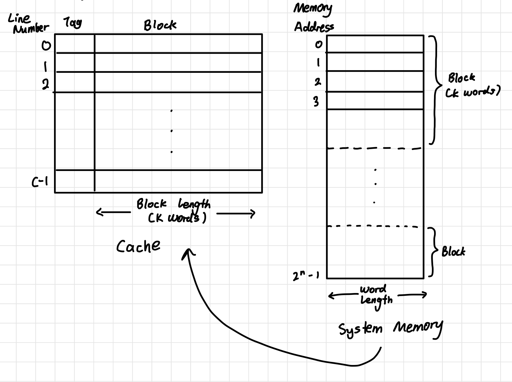
How content of System Memory is stored in cache
System memory is divided into fixed-sized blocks, and the cache is organised into cache lines of the same size. Each cache line can store exactly one memory block. When the CPU accesses the address, the cache is checked to see if the block containing that address is already present. If it is not found, the memory block is fetched from the system memory and copied into the selected cache line. Along with the data, a tag is stored in the cache line, which identifies the specific memory block currently held there. This tag allows the CPU to verify whether the correct block is stored in taht cache line during future accesses.
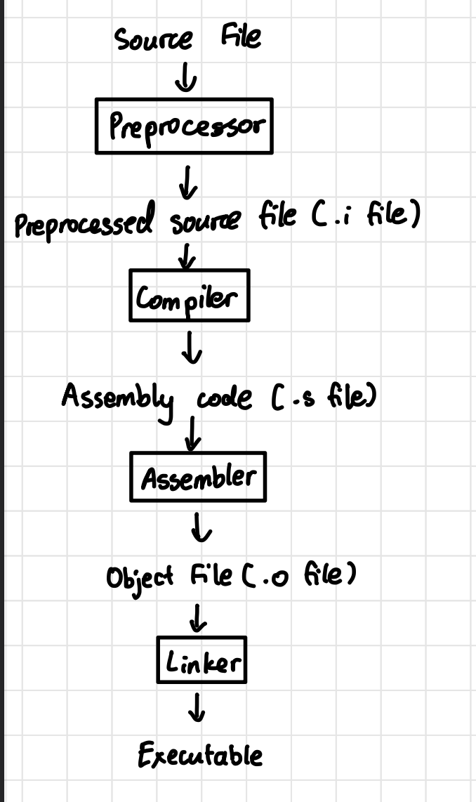
Compilation Process Block Diagram
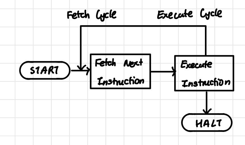
Fetch Execute /Instruction Cycle Block Diagram (without interrupts)
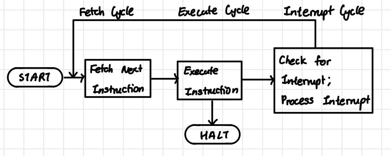
Fetch Execute / Instruction Cycle Block Diagram (with interrupts)
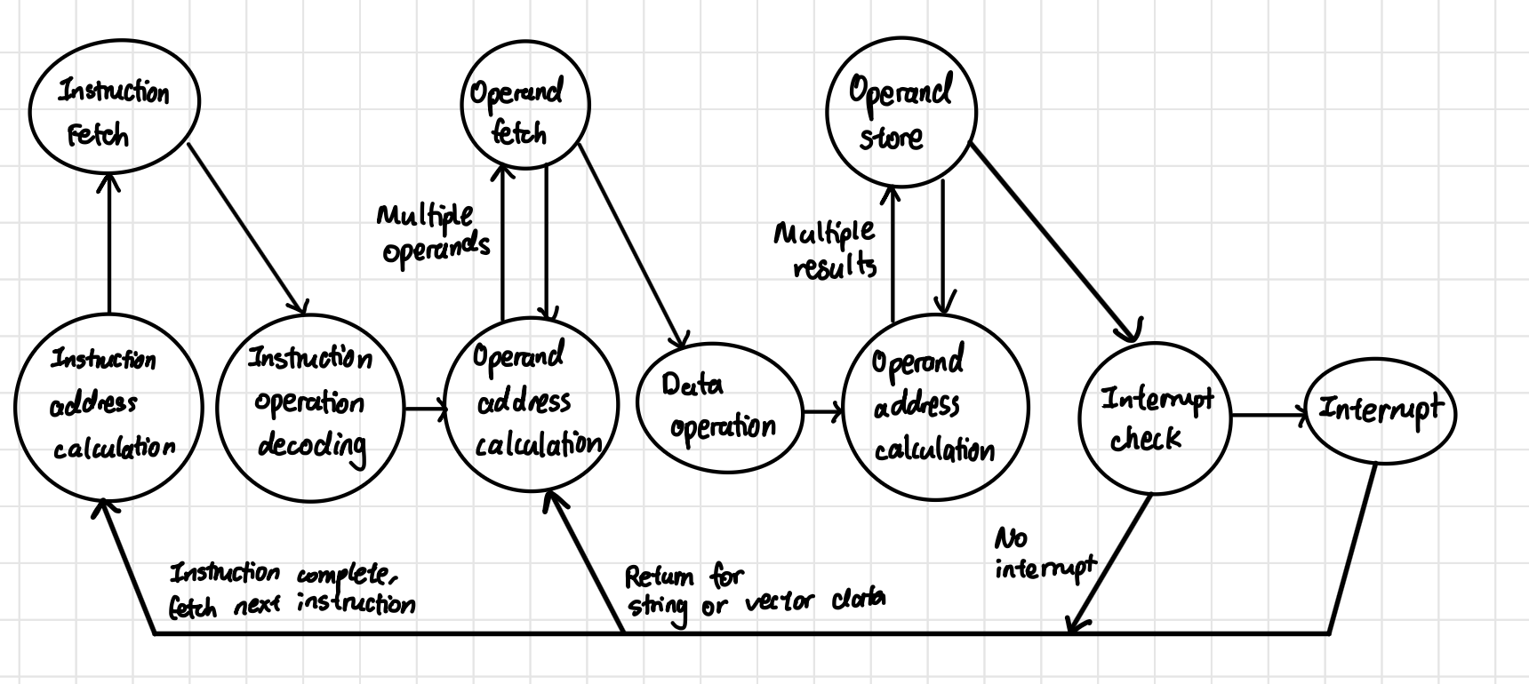
Instruction Cycle State Diagram (with interrupts)
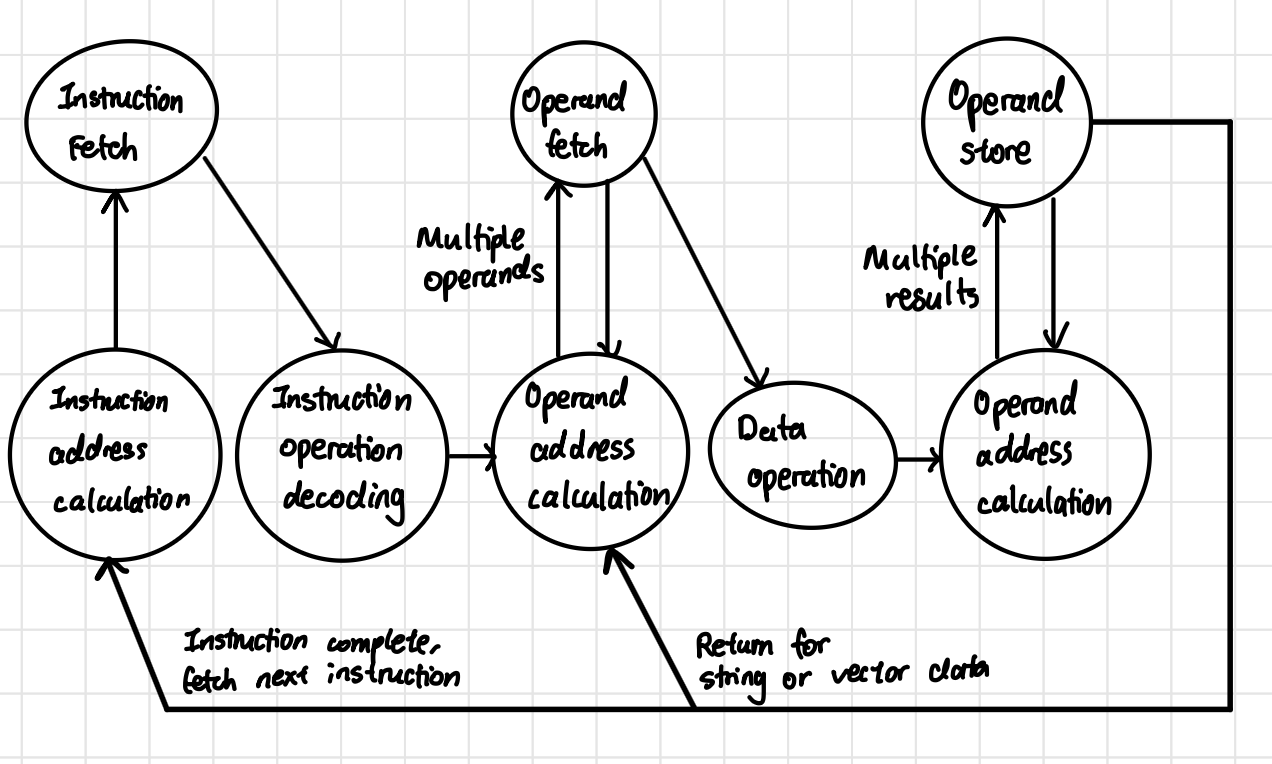
Instruction Cycle State Diagram (without interrupts)
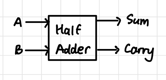
Half Adder Block Diagram
Half Adder Circuit Diagram
Half Adder Truth Table

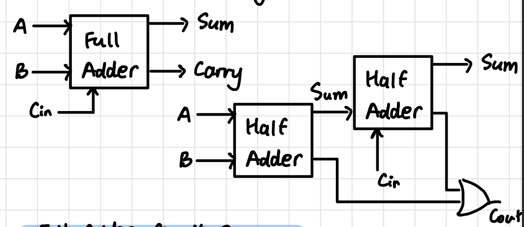
Full Adder Block Diagram
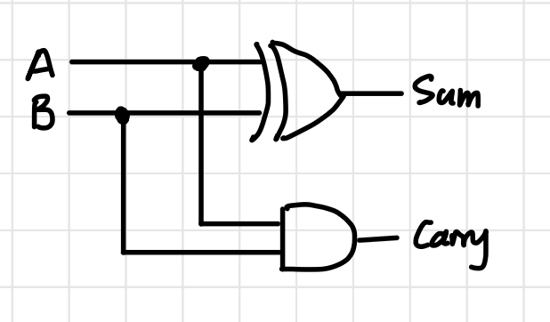
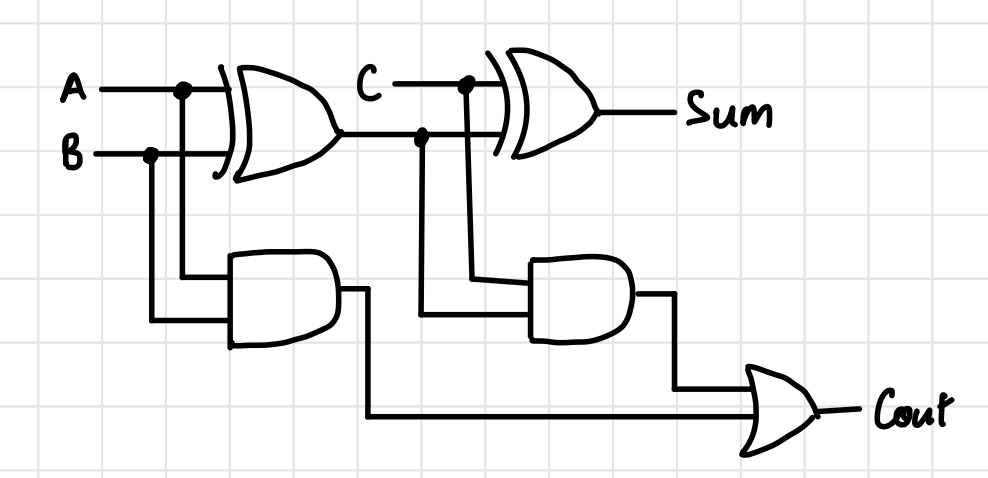
Full Adder Circuit Diagram
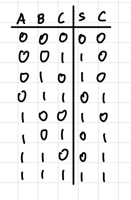
Full Adder Truth Table
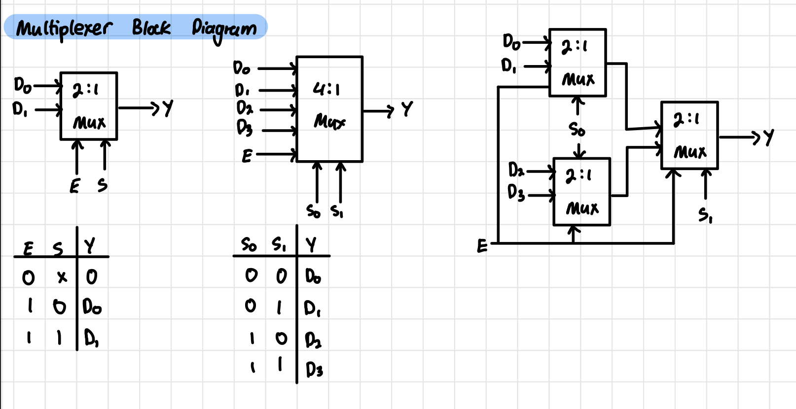
Multiplexer Block Diagram
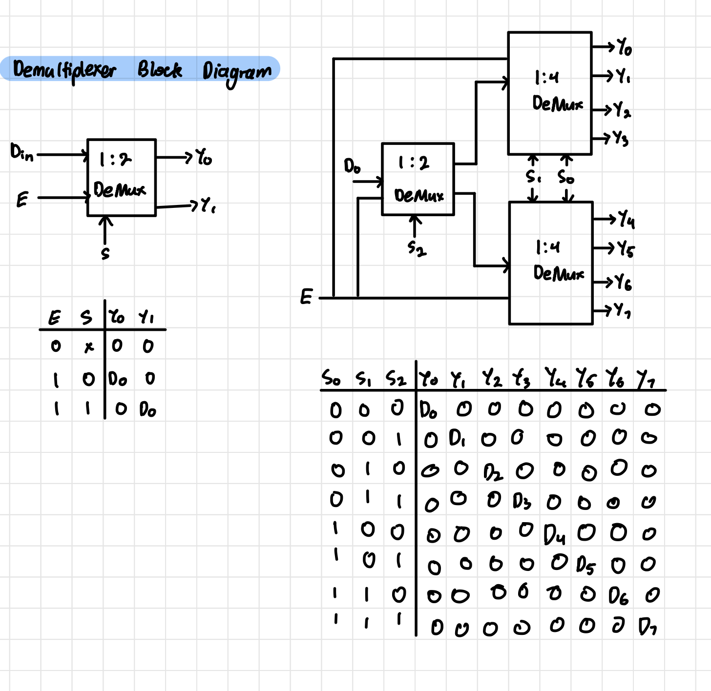
Demultiplexer Block Diagram
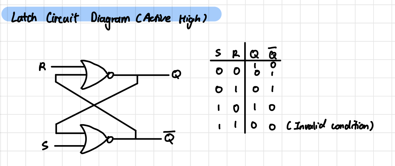
Latch Circuit Diagram (Active High)
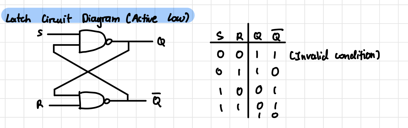
Latch Circuit Diagram (Active Low)
SR Flip Flop Circuit Diagram

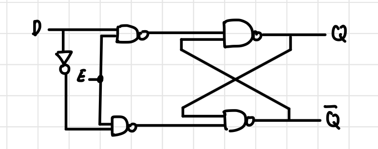
D Flip Flop Circuit Diagram
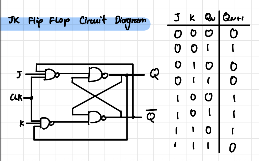
JK Flip Flop Circuit Diagram
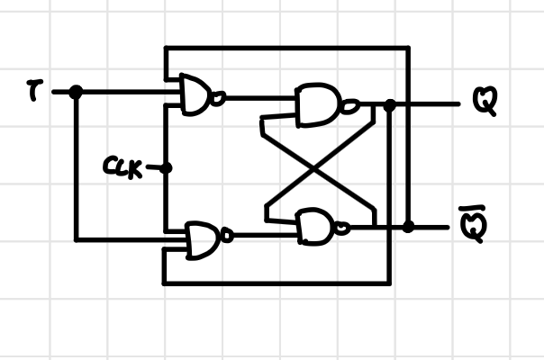
T Flip Flop Circuit Diagram
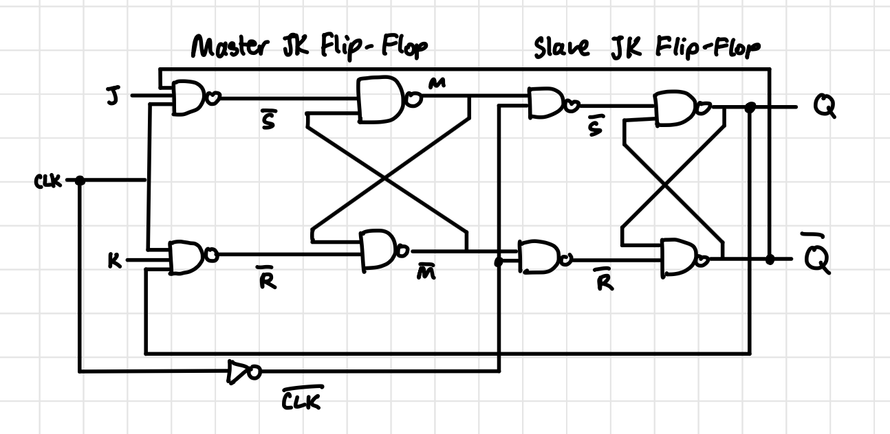
Master-Slave JK Flip Flop Circuit Diagram
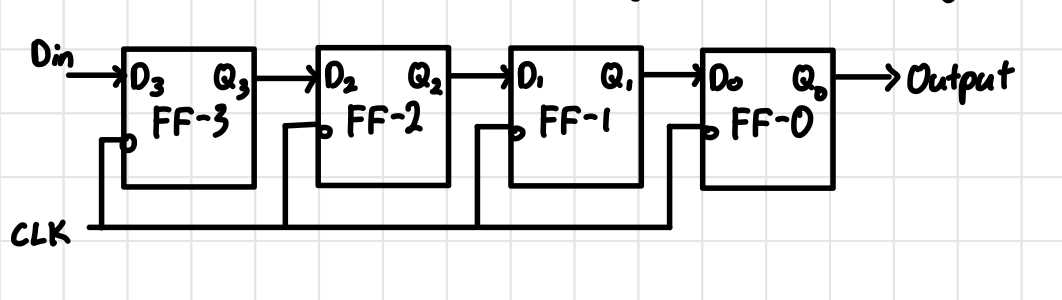
SISO Block Diagram
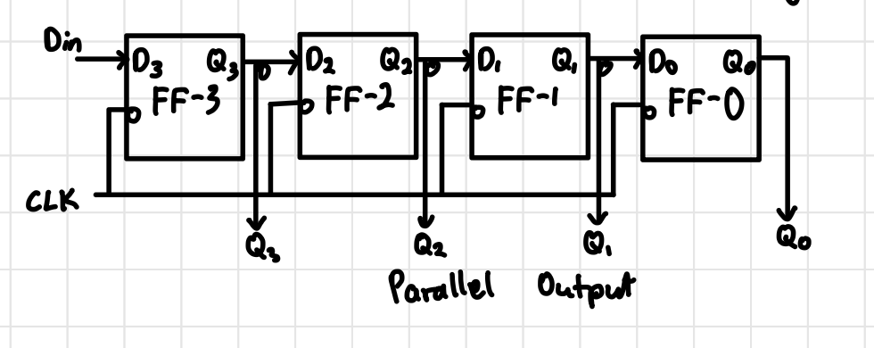
SIPO Block Diagram
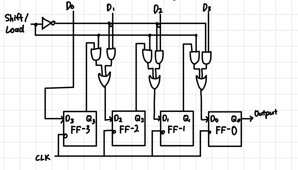
PISO Block Diagram
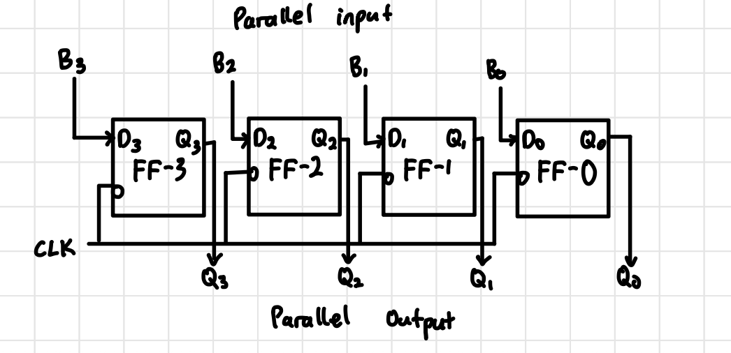
PIPO Block Diagram
I/O Module Block Diagram

I/O Controller Block Diagram

Cache and System Memory Diagram