Electron microscopy - revision
1/14
There's no tags or description
Looks like no tags are added yet.
Name | Mastery | Learn | Test | Matching | Spaced |
|---|
No study sessions yet.
15 Terms
what is an electron?
An electron is a negatively charged subatomic particle that orbits the nucleus of an atom. In chemistry, electrons are essential for chemical bonding, determining how atoms interact to form molecules. They occupy energy levels or orbitals, and the arrangement of electrons in these orbitals governs an element’s reactivity, valency, and placement in the periodic table. Electrons are involved in ionic and covalent bonding, redox reactions, and the flow of electricity in conductive materials.
symbol: e-
2.Calculate the wavelength of electrons being accelerated through 50kV.
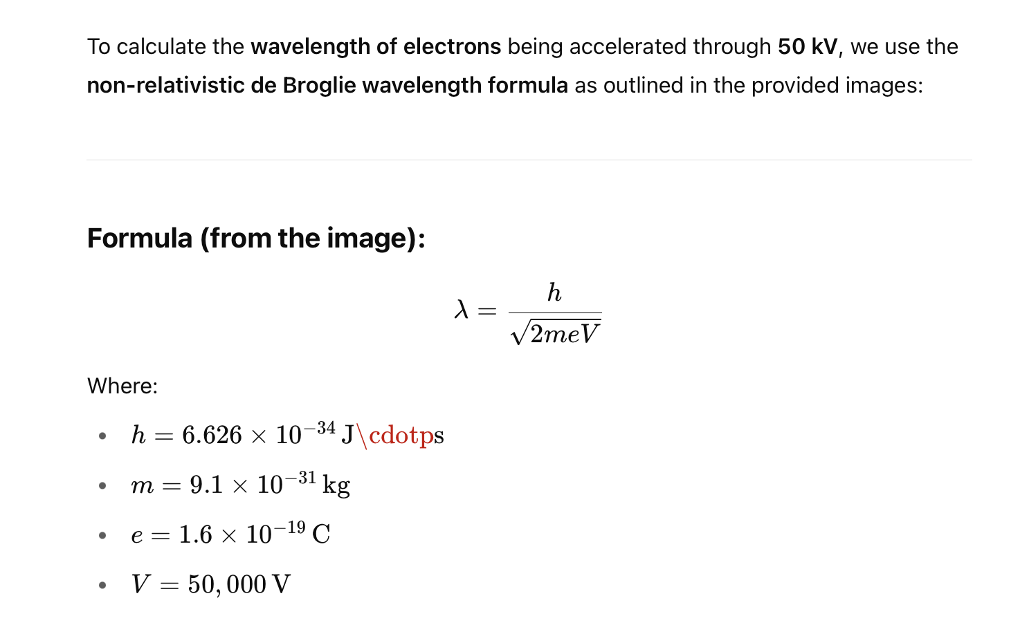
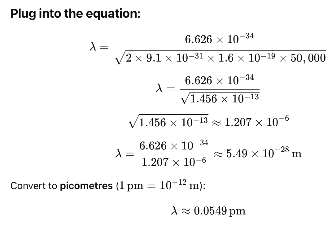
✅ Answer:
The de Broglie wavelength of electrons accelerated through 50 kV is approximately 0.055 picometres (pm).
Note: This is a non-relativistic estimate. For more accurate values at high voltages (like 50 kV and above), relativistic corrections should be applied as shown in the lower boxed formula on the second image. Let me know if you'd like that version calculated too.
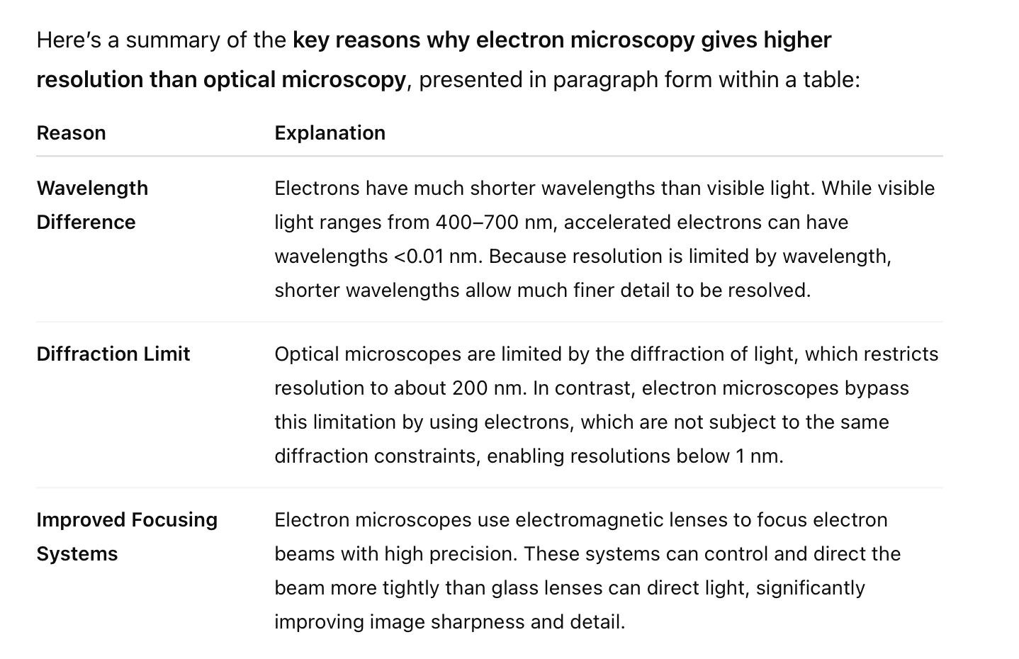
Why does electron microscopy give much higher resolution than optical microscopy?
Electron microscopy gives much higher resolution than optical (light) microscopy because electrons have a much shorter wavelength than visible light, and resolution is fundamentally limited by the wavelength of the imaging source.
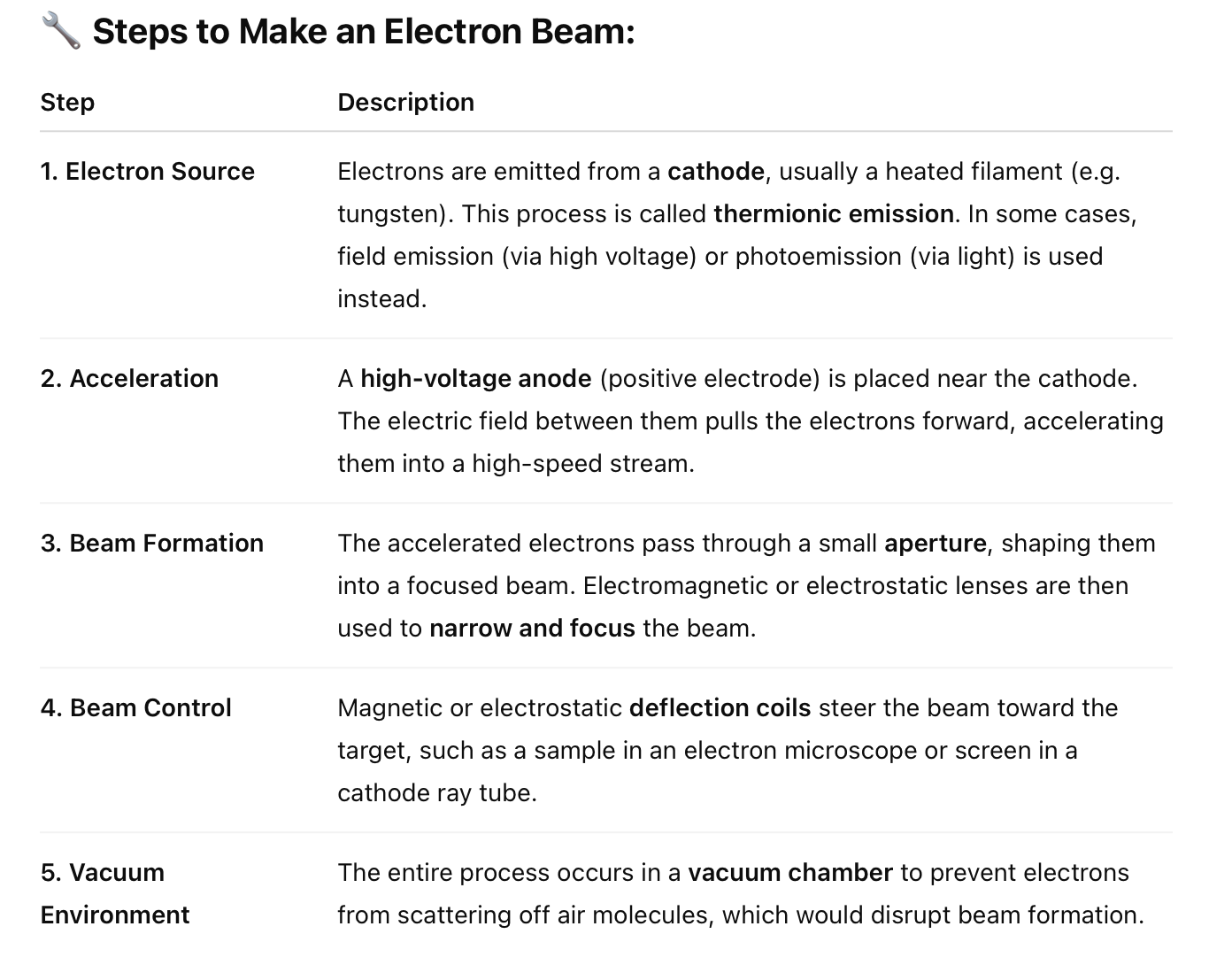
How do you make an electron beam?
An electron beam is produced by generating free electrons and accelerating them using electric fields, typically inside a vacuum. Here's how it's done step by step:
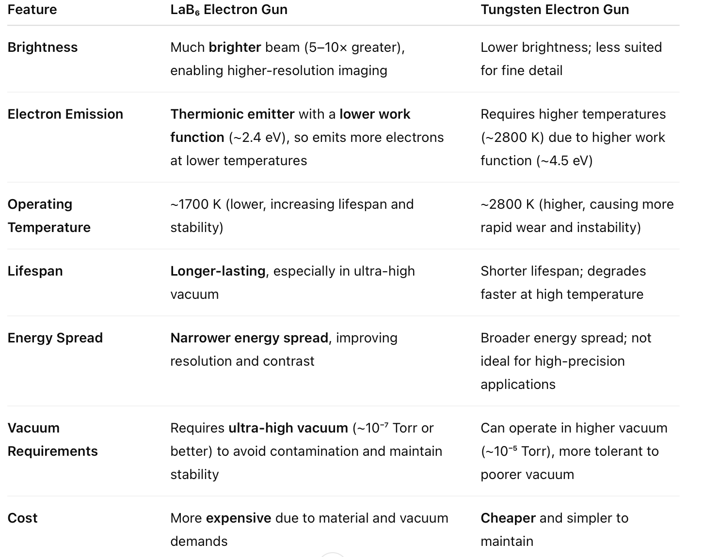
Why is a LaB6 electron gun better than a W gun?
A LaB₆ (lanthanum hexaboride) electron gun is considered better than a tungsten (W) filament gun in many applications because it offers superior performance in several key areas:
✅ Summary:
A LaB₆ gun is better because it delivers:
Brighter, more stable beams
Sharper images and higher resolution
Greater efficiency at lower temperatures
However, it needs a cleaner vacuum system and costs more, which can be a trade-off in simpler or lower-budget instruments.
How can you control an electron beam?
Controlling an electron beam involves manipulating its trajectory, focus, and position using electric and magnetic fields.These methods are fundamental in devices like electron microscopes, cathode ray tubes (CRTs), and particle accelerators.
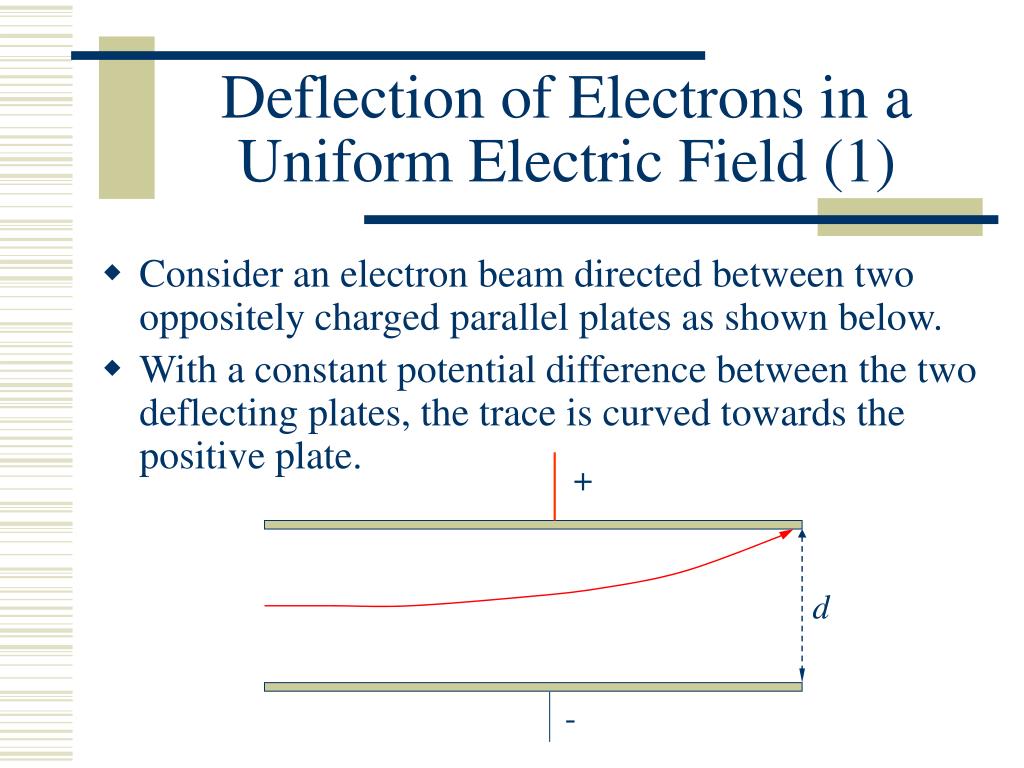
Electric Field Deflection
Mechanism: By placing two oppositely charged plates on either side of the electron beam, an electric field is created perpendicular to the beam's path. The electrons experience a force due to this field, causing the beam to deflect toward the positively charged plate.
Application: This principle is utilized in CRTs to direct the electron beam across the screen, forming images.EBM Machine
Magnetic Field Deflection
Mechanism: When an electron beam passes through a magnetic field perpendicular to its direction of motion, it experiences the Lorentz force, causing it to move in a circular or helical path.
Application: Magnetic deflection is employed in oscilloscopes and certain types of electron microscopes to steer the beam accurately.
Electromagnetic Lenses
Mechanism: Electromagnetic lenses use magnetic fields generated by coils to focus and shape the electron beam, similar to how optical lenses focus light.
Application: These lenses are crucial in electron microscopes for achieving high-resolution imaging by focusing the electron beam onto the specimen.
Deflection Coils (Rastering)
Mechanism: Deflection coils generate varying magnetic fields that can rapidly change the direction of the electron beam, allowing it to scan across a surface in a controlled pattern.
Application: This technique is used in scanning electron microscopes (SEMs) to systematically scan the electron beam over the sample surface for imaging.Dexter Magnetic Technologies
Stigmators
Mechanism: Stigmators apply weak, adjustable magnetic or electric fields to correct asymmetries in the electron beam, reducing astigmatism and improving image clarity.
Application: They are essential in fine-tuning the beam in high-resolution electron microscopy.Wikipedia+1Global Sino+1
📺Visual Demonstration
For a practical demonstration of electron beam deflection using magnetic fields, you can watch the following video:
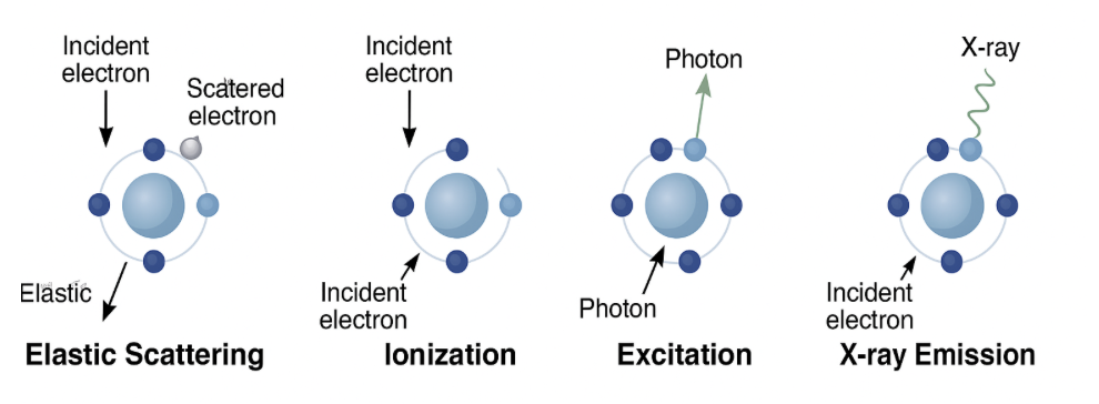
When an electron beam interacts with matter, what can happen to the atoms and molecules in the sample? Define the processes using diagrams at the atomic scale.
1. Elastic Scattering
In elastic scattering, an incident electron interacts with the electric field of an atom—usually the nucleus—without transferring significant energy. The electron changes direction but retains nearly all its original energy. This process affects the trajectory of the beam and contributes to image contrast in electron microscopy.
2. Ionization
Ionization occurs when the incident electron transfers enough energy to eject an inner-shell electron from the atom. This leaves the atom ionized (positively charged) and creates a vacancy in an electron shell, which can lead to secondary effects like X-ray emission or Auger electron release. Ionization is a key process in generating electron energy loss spectra.
3. Excitation
In excitation, the incident electron transfers part of its energy to an atomic electron, promoting it to a higher energy level without ejecting it from the atom. The excited electron eventually falls back to its original state, releasing energy as a photon—typically a visible or ultraviolet photon depending on the energy transition.
4. X-ray Emission
X-ray emission follows ionization when a higher-energy electron drops down to fill the inner-shell vacancy. The energy difference is released as a characteristic X-ray photon. This process forms the basis of Energy Dispersive X-ray Spectroscopy (EDS), which is used to identify the elemental composition of materials.
In electron microscopy, what is the reaction volume and factors determine its size? How big are these reaction volumes.
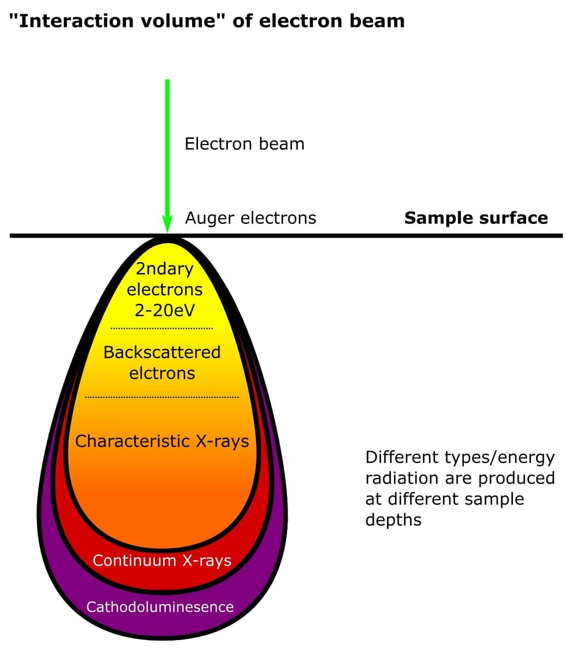
Reaction Volume in Electron Microscopy
In electron microscopy, the reaction volume—also called the interaction volume—is the 3D region within a samplewhere incident electrons interact with atoms. It defines the zone where signals like secondary electrons, backscattered electrons, X-rays, and Auger electrons are generated.
Size of the Reaction Volume
The size ranges from a few nanometres to several micrometres, depending on various factors.
In Transmission Electron Microscopy (TEM): the interaction volume is extremely small (~1–10 nm), as electrons pass through thin specimens.
In Scanning Electron Microscopy (SEM): the interaction volume can reach up to 1–5 micrometres, especially in bulk specimens.
Factors That Determine Reaction Volume Size
Factor | Effect on Reaction Volume |
|---|---|
Accelerating Voltage | Higher voltages increase electron penetration depth, expanding the reaction volume. |
Atomic Number (Z) | Higher-Z materials scatter electrons more, reducing penetration and shrinking the volume. |
Sample Density | Denser materials absorb more energy, leading to smaller interaction volumes. |
Beam Spot Size | A finer beam creates a more localized reaction volume, especially important for high-resolution imaging. |
Electron Scattering | Both elastic and inelastic scattering broaden the volume shape, especially in SEM, forming a "teardrop" or "pear-shaped" zone. |
Summary:
The reaction volume is crucial for interpreting resolution and signal origin in electron microscopy.
It is typically larger in SEM (up to microns) and much smaller in TEM (nanometres).
Controlled by beam energy, material properties, and beam focus, this volume limits spatial resolution, especially for X-ray and backscattered signals.
A pure element in SEM can produce many lines in the spectrum. Why?
In Scanning Electron Microscopy (SEM), a pure element can produce many lines in its X-ray spectrum due to the presence of multiple electron shells and allowed electronic transitions within the atom. These spectral lines are known as characteristic X-ray peaks.
Why This Happens:
Multiple Electron Shells (K, L, M...)
Atoms have several energy levels (shells), such as the K-shell (1s), L-shell (2s, 2p), and M-shell (3s, 3p, 3d). When an incident electron knocks out an inner-shell electron (e.g., from the K-shell), an electron from a higher shell falls down to fill the vacancy.Each Transition Releases a Photon
The energy difference between the shells is emitted as an X-ray photon, and this energy is specific to the element and the shells involved.Many Possible Transitions
A single element can produce:Kα lines: transition from L → K shell
Kβ lines: M → K shell
Lα, Lβ...: transitions involving L and M shells, etc.
Resulting Spectrum
The X-ray Energy Dispersive Spectrum (EDS or EDX) of a pure element will show multiple peakscorresponding to each of these transitions, despite being from just one type of atom.
Example:
For iron (Fe), you might see:
Kα line at ~6.4 keV
Kβ line at ~7.1 keV
Possibly L lines if low-energy X-rays are detectable
Summary:
A pure element produces many lines in an SEM spectrum because each electron shell can participate in distinct characteristic X-ray emissions. These multiple electronic transitions result in a spectrum with several sharp peaks, even from a single element.
What do the signals generated by the electron beam/specimen interaction reveal about the
sample.
When an electron beam interacts with a specimen in electron microscopy, it generates several types of signals. Each signal provides different, complementary information about the composition, structure, and topography of the sample:
Signals and What They Reveal:
Signal | What It Reveals About the Sample |
|---|---|
Secondary Electrons (SE) | Provide high-resolution surface topography. These low-energy electrons are emitted from near the surface, showing fine surface details. |
Backscattered Electrons (BSE) | Reveal atomic number contrast (Z-contrast). Heavier elements backscatter more electrons, so they appear brighter, helping to identify phase distribution. |
Characteristic X-rays (EDS/EDX) | Reveal the elemental composition. Each element emits specific X-ray energies when inner-shell electrons are replaced, allowing qualitative and quantitative analysis. |
Auger Electrons | Provide surface chemical composition with nanometre-scale depth sensitivity, useful in surface science and materials analysis. |
Transmitted Electrons (TEM) | Give internal structure and crystallography. These electrons pass through thin specimens and form high-resolution images (down to atomic scale). |
Electron Energy Loss (EELS) | Reveal chemical bonding, oxidation states, and light element content, especially in Transmission Electron Microscopy (TEM). |
Summary:
The various signals generated by electron–specimen interaction offer a multidimensional picture of the sample:
SE → Surface detail
BSE → Composition contrast
X-rays (EDS) → Elemental identification
Auger → Surface chemistry
TEM signals → Atomic structure
EELS → Chemical and electronic environment.

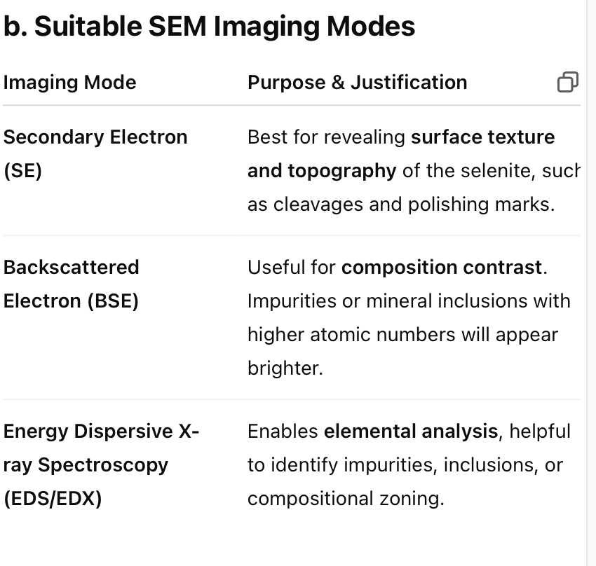
The picture below shows a polished piece of selenite crystal. Does not look very pure!
a. How would you prepare the sample for scanning electron microscopy?
b. Which imaging modes would be most suited for the analysis of the sample?
analysis of a polished selenite crystal-
While the selenite appears impure or inhomogeneous in the image, Scanning Electron Microscopy (SEM) can reveal far more about its microstructure and composition. Here's how you'd approach it:
Sample Preparation for SEM
Sectioning (if needed)
Cut a small, flat piece (~5–10 mm) from the selenite sample to fit into the SEM chamber.Mounting
Secure the sample onto an aluminium stub using conductive carbon tape or glue.Surface Cleaning
Use compressed air, ethanol rinse, or ultrasonic cleaning to remove dust or oils without altering the surface structure.Coating (if non-conductive)
Since selenite is insulating, coat the surface with a thin layer of conductive material (e.g. gold, carbon, or platinum) using sputter coating. This prevents charging and improves image quality.Vacuum Insertion
Place the sample into the SEM vacuum chamber for imaging.
Summary:
Preparation: Clean, mount, and sputter-coat the selenite for SEM.
Best imaging modes: Use SE for surface detail, BSE for compositional contrast, and EDS to identify non-selenite inclusions.
Why is DNA difficult to analyze using SEM.
DNA is difficult to analyze using Scanning Electron Microscopy (SEM) due to several key challenges related to its physical, chemical, and electrical properties:
1. Non-conductive Nature
DNA is non-conductive, so when it's exposed to an electron beam in SEM, it accumulates charge (called charging). This distorts the image and can damage the sample. Conductive coating (e.g. gold or carbon) is required, but that can mask fine structural details.
2. Highly Sensitive to Electron Beam Damage
DNA is composed of delicate organic molecules that are easily damaged or broken by the high-energy electrons in SEM. This can lead to structural changes, fragmentation, or complete loss of the sample’s form.
3. Requires Dehydration
SEM operates in a vacuum, but DNA naturally exists in a hydrated state in cells or solutions. Removing water can cause the DNA to collapse, denature, or aggregate, making it difficult to maintain its native structure.
4. Small Size and Low Atomic Number
DNA is extremely thin (~2 nm diameter) and composed mainly of light elements (C, H, O, N, P). These elements produce weak electron signals, resulting in poor contrast and low signal-to-noise ratio in SEM images.
5. Complex Sample Preparation
To preserve the native shape of DNA under SEM, extensive preparation is required: fixation, dehydration, drying, and coating. This is time-consuming and may introduce artefacts.
Because of these challenges, Atomic Force Microscopy (AFM) or Transmission Electron Microscopy (TEM) is often preferred for imaging DNA at the nanoscale.
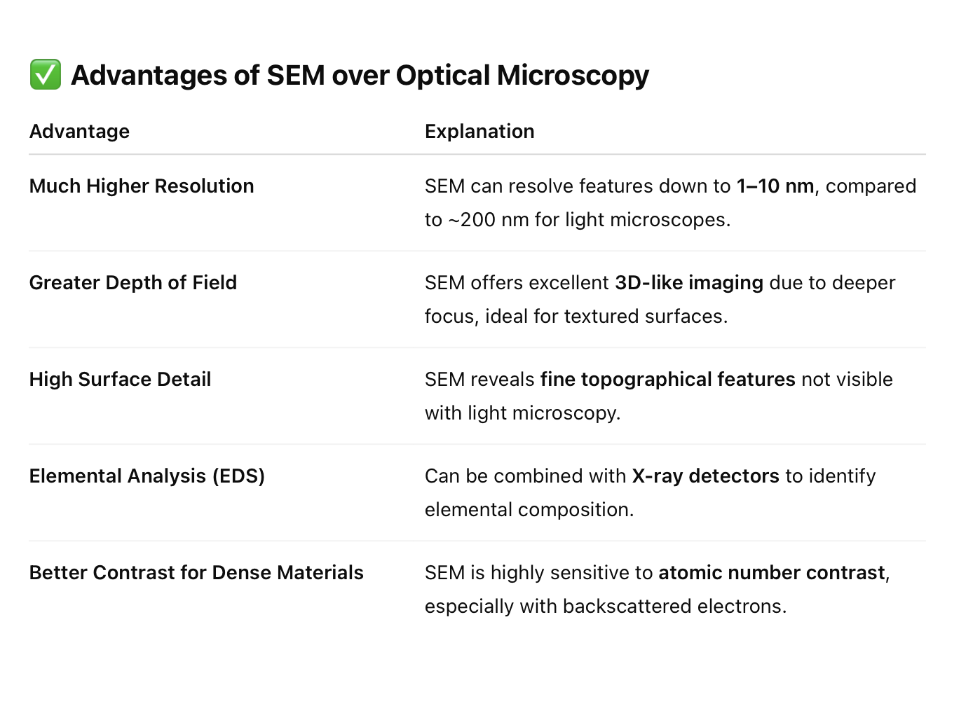
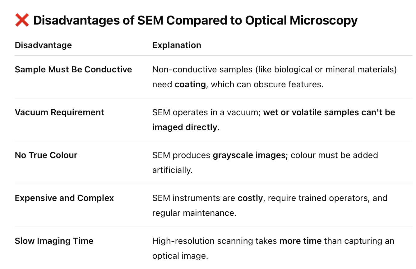
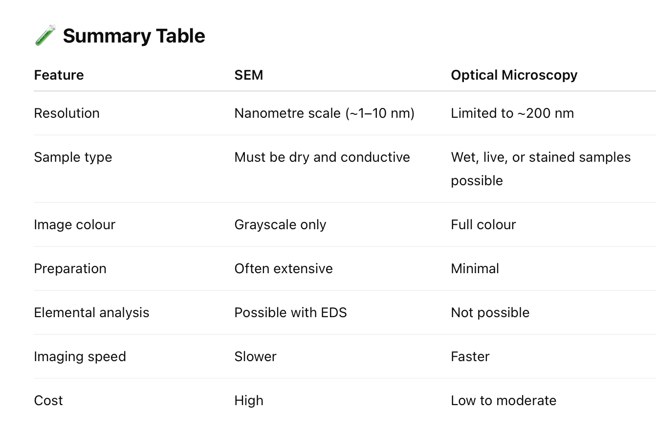
State the advantages and disadvantages of SEM when compared optical microscopy.