scanning probe microscopy part 3 - (SPM) scanning tunnelling
1/17
There's no tags or description
Looks like no tags are added yet.
Name | Mastery | Learn | Test | Matching | Spaced |
|---|
No study sessions yet.
18 Terms
Theory
Introduction:
STM was the first SPM.


Electron tunnelling (Quantum)
electrons have wave-particle duality.
electron tunnelling is a quantum mechanical effect.
A tunnelling current occurs when electrons move through a barrier that they classically shouldn’t be able to move through.
In classical terms, if you don’t have enough energy to move “over” a barrier, you won’t.
Tunnel Effect
When a quantum object is sent on a thick barrier, it bounces off.
If the barrier is thin enough the object may sometimes get through.
the thinner the barrier the more likely the object to pass.
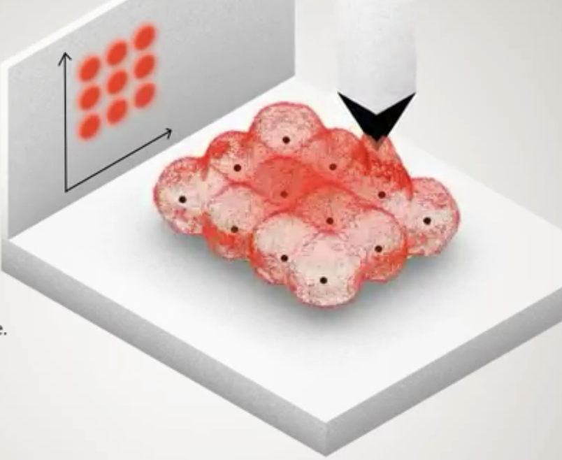
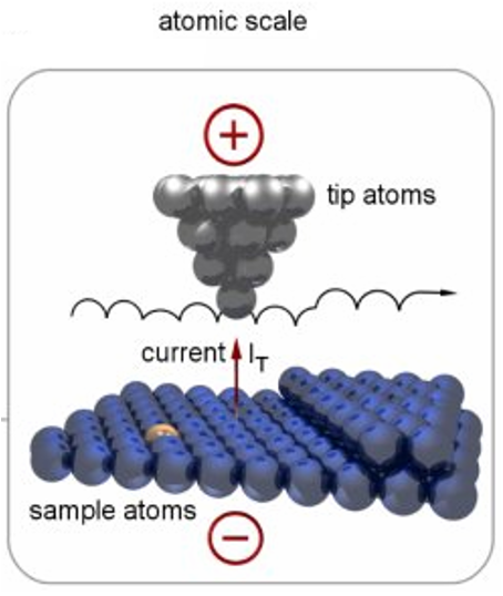
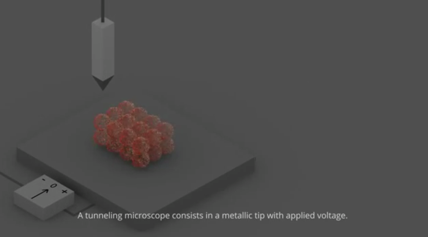
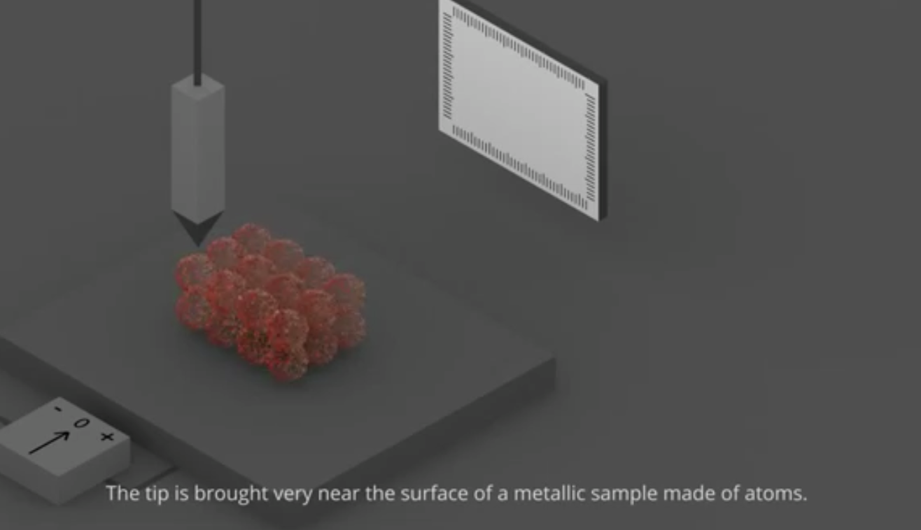
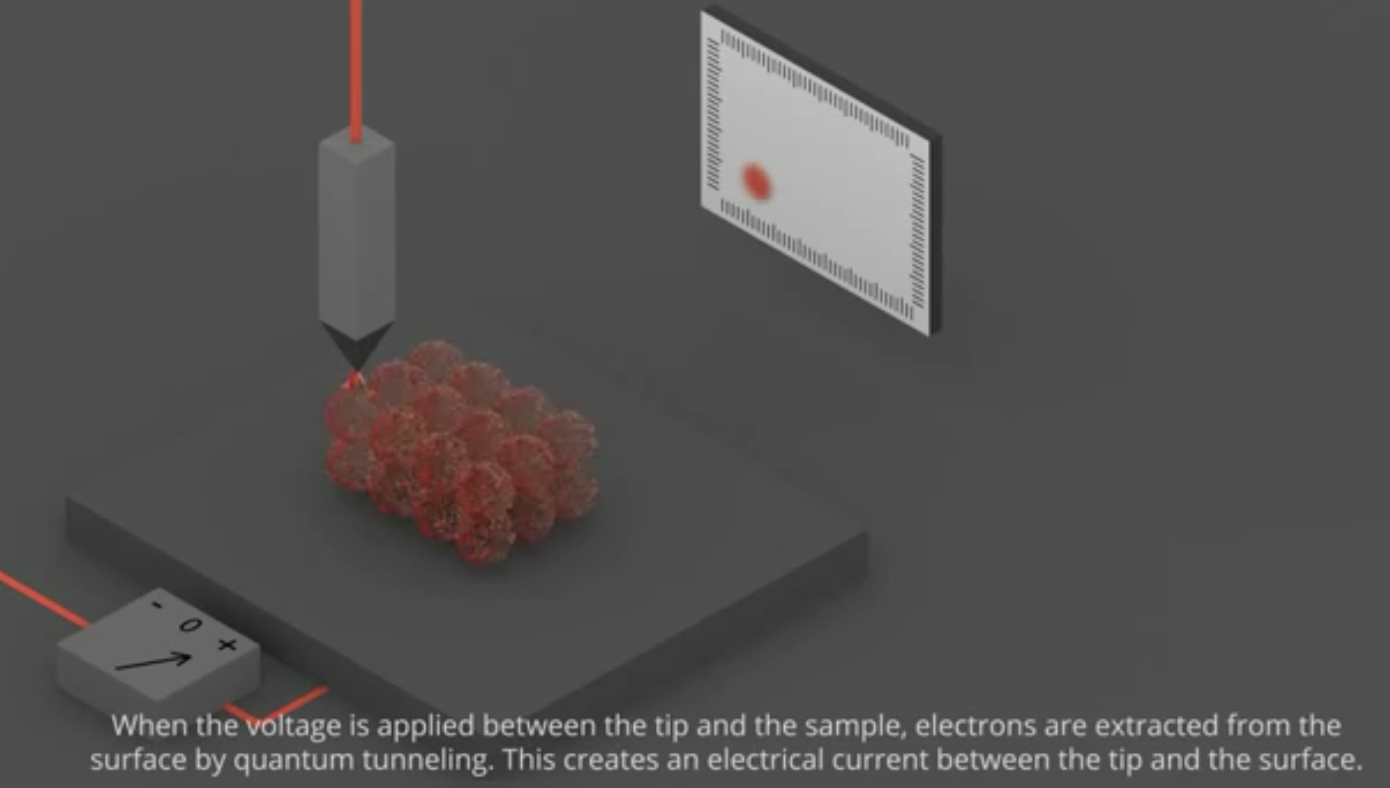
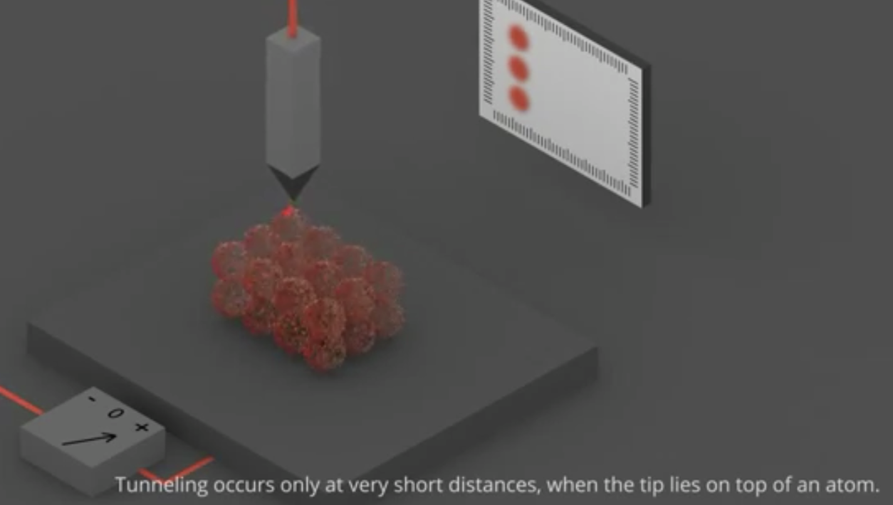
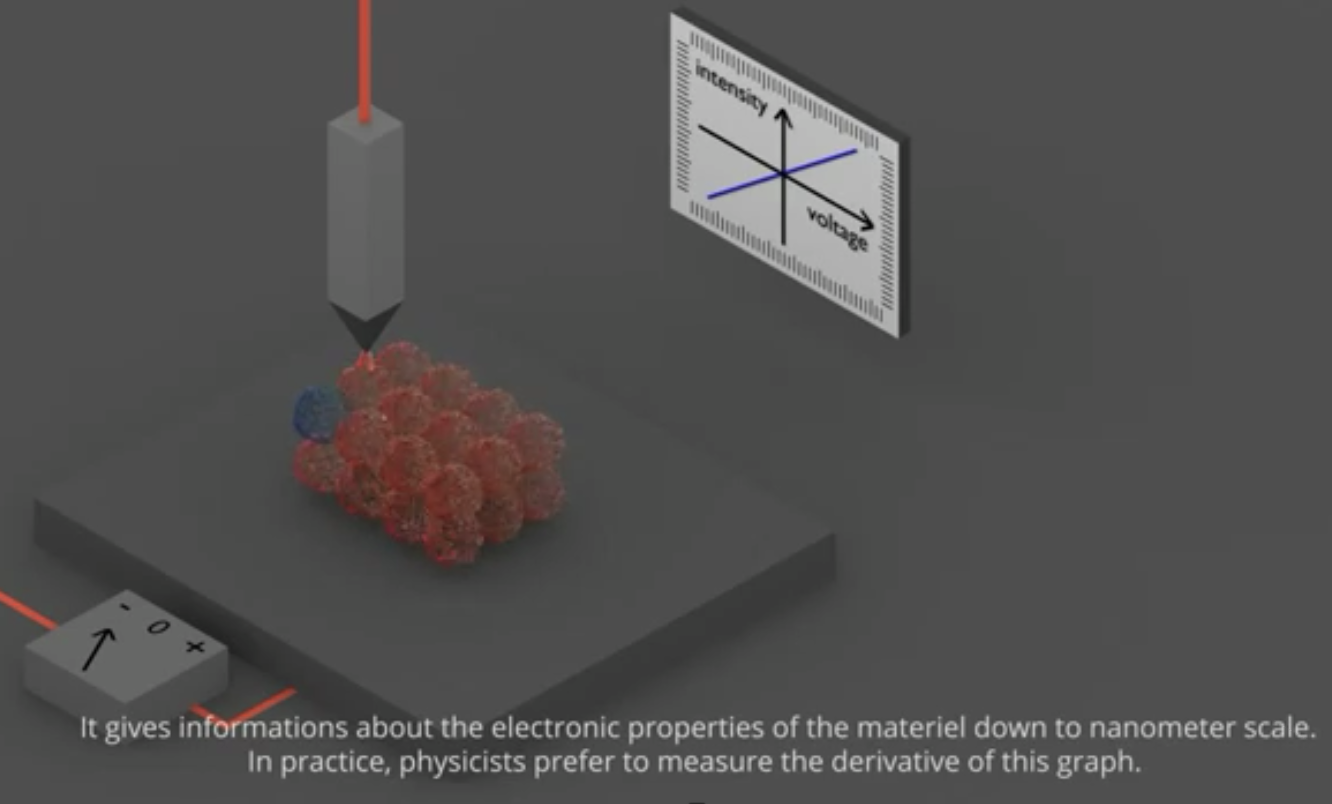
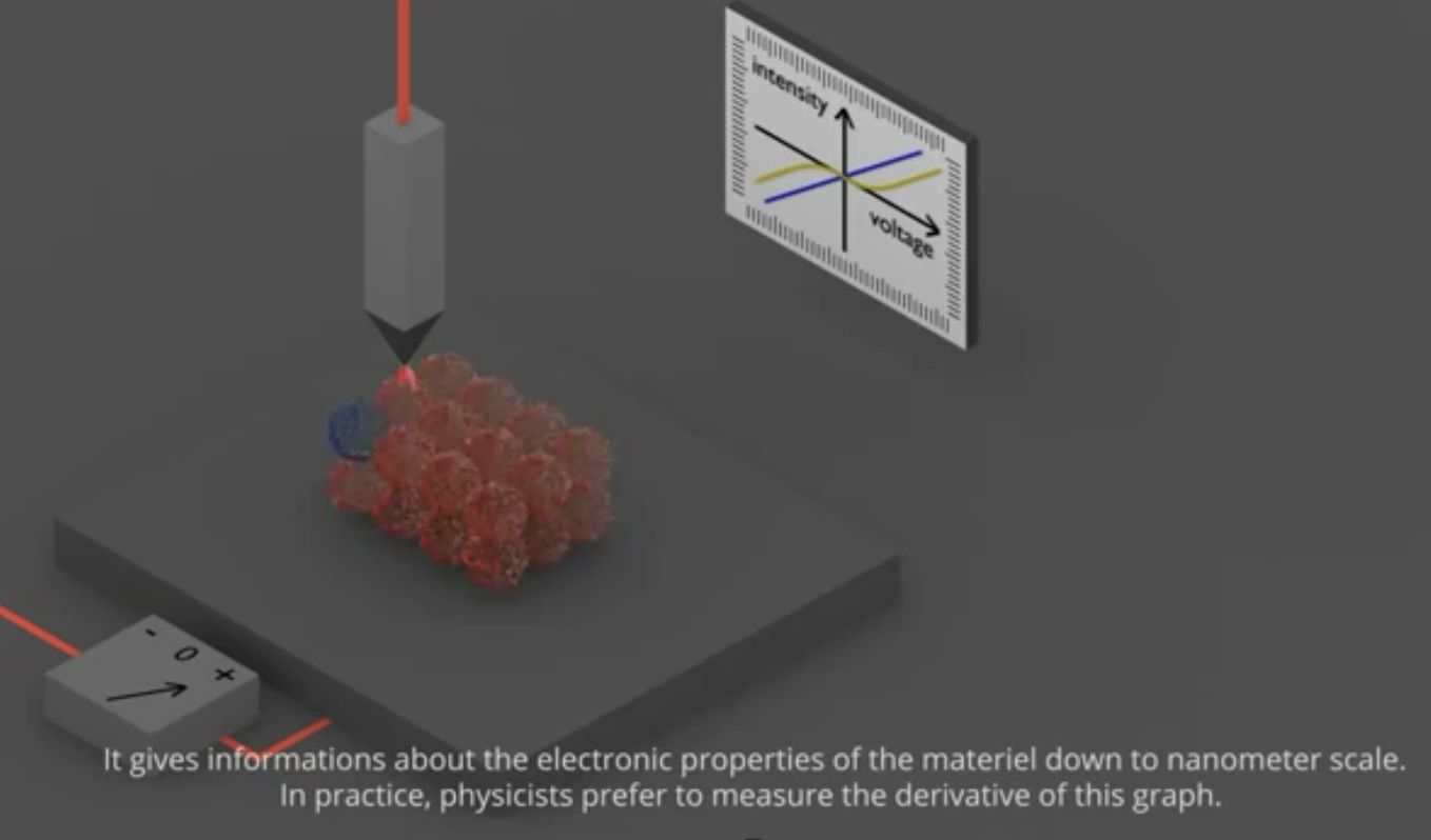
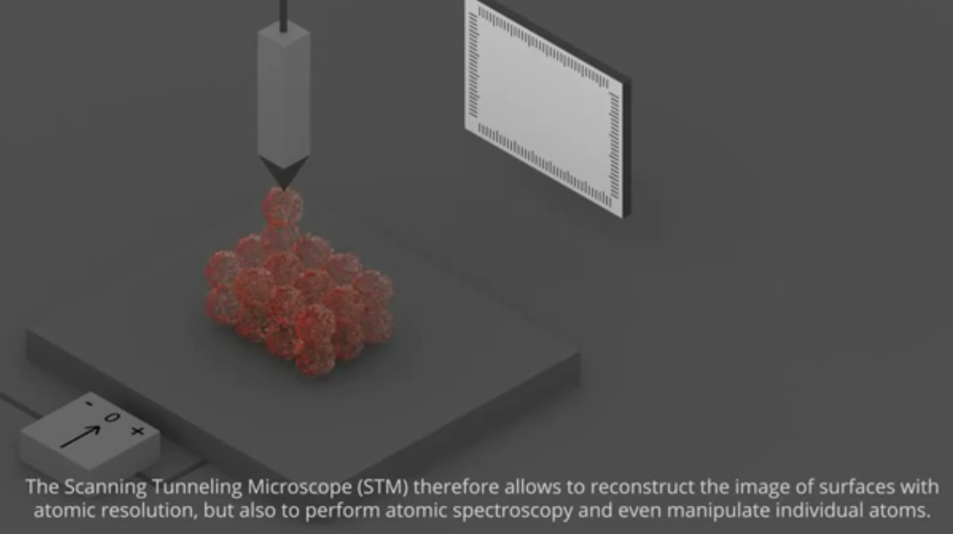
A metal is made up of quantum atoms and electrons. If we approach a very thin tip electrically powered, it may tear the electrons from the metal by tunnel effect.
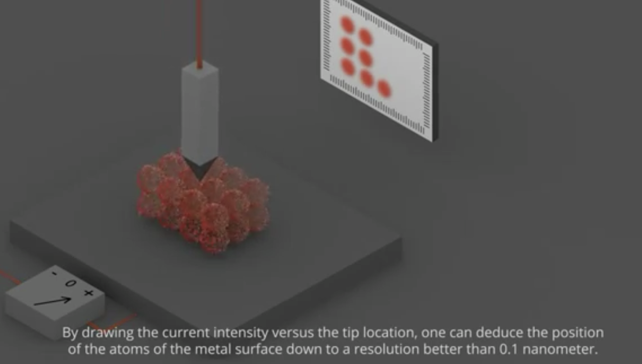
By measuring the electric current passing through the tip, we can reconstruct where the atoms are.
This is the principle of the scanning tunnelling microscope.
in the quantum mechanical world, electrons have wave-like properties.
These waves don’t end abruptly at a wall or barrier, but taper off quite quickly.
If the barrier is thin enough, the probability function may extend into the next region, through the barrier.
when an electron moves through the barrier in this function, it is called tunnelling.
Instrumentation
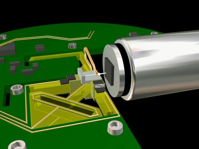
Tips
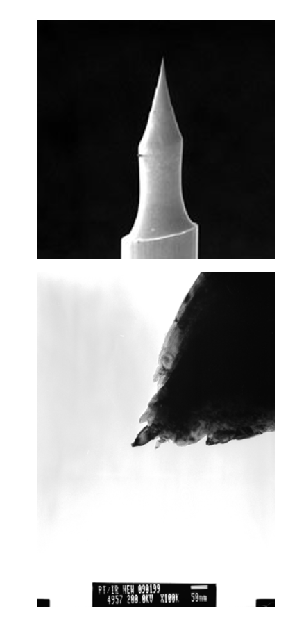
STM tips are formed from tungsten wire by chemical etching.
Tips diameter approx. 0.0025mm.
For atomic imaging mechanically formed Pt/Ir tips are used.
Tip length is 8mm.
Theory
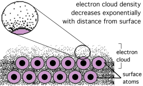
according to quantum mechanics, electrons on a surface behave like an “electron cloud”.
The electron density of the cloud decreases exponentially with distance from the surface.
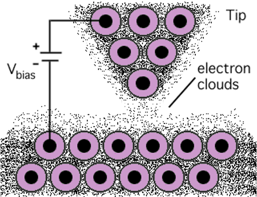
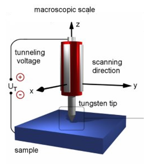
The STM initiates tunnelling by positioning its tips (a conductor) within a few Angstroms of the surface (also a conductor).
The strong dependence of the tunnelling current with the tip-sample distance is described by the equation:
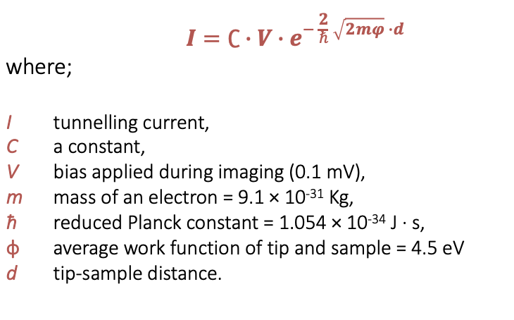
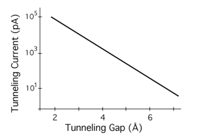
The relationship of tunnelling current to tip distance for a single bias voltage:
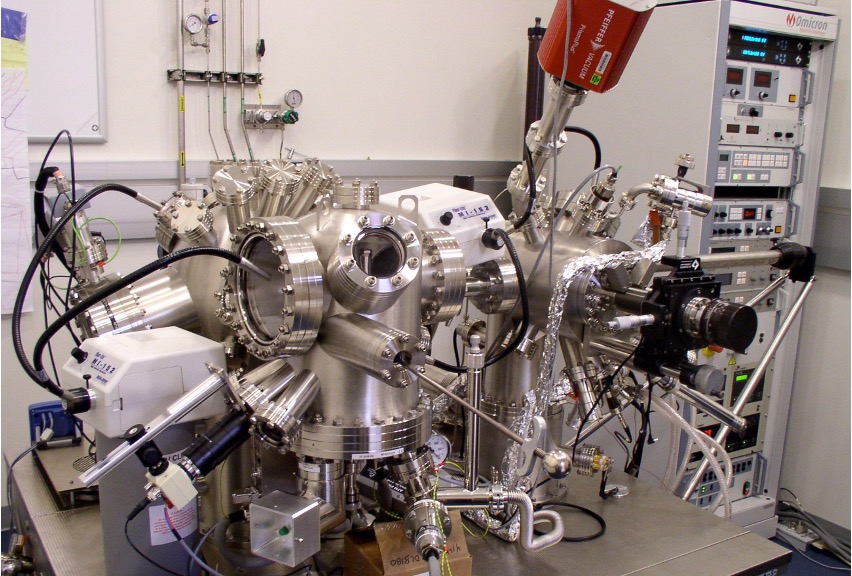
STM design
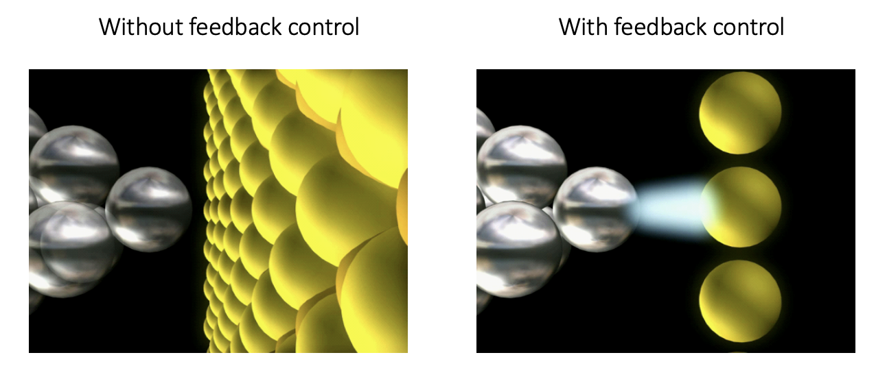
Precision control
the tip-to-sample distance must be under control of the instrument, without interference from noise, vibration, thermal effect, etc.
the instrument must have precise, stable position control, with Angstrom-level resolution, to prevent a “crash” of the tip into the sample.
Measurement
the STM must sense extremely small currents, in the pA range.
Sample
Sample must exhibit electrically conducting.
STM Design
STM Control
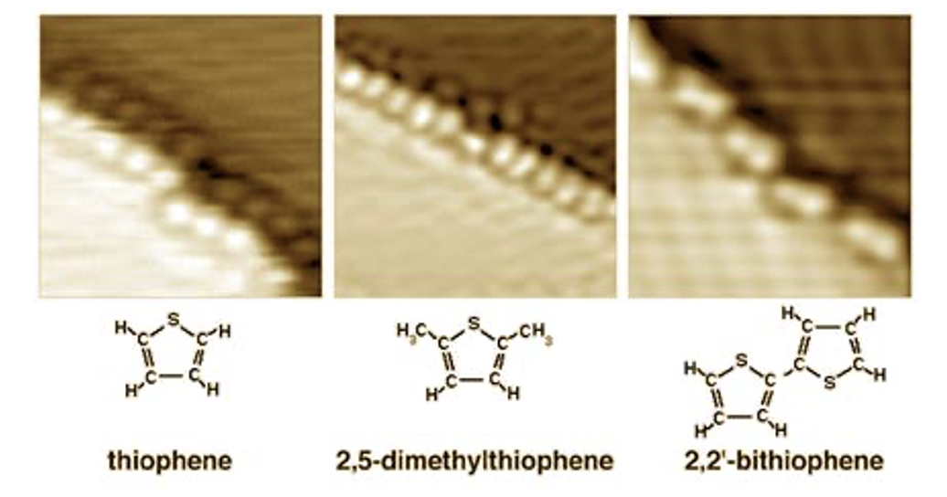
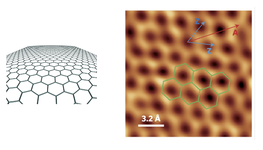
Application
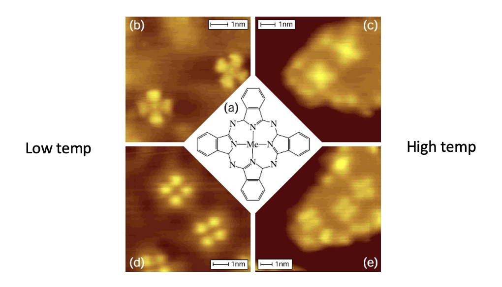
STM of Graphene
Low temperature STM