Diode Review and Concepts for ESET 350 Course
1/98
There's no tags or description
Looks like no tags are added yet.
Name | Mastery | Learn | Test | Matching | Spaced |
|---|
No study sessions yet.
99 Terms
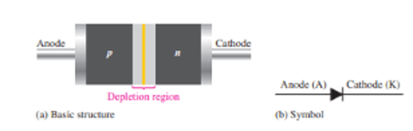
What is the diagram for a diode and its corresponding regions?
The p region is called the anode
The n region is called the cathode
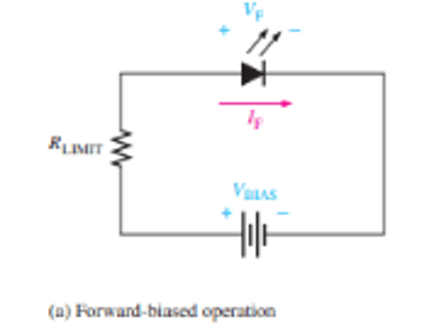
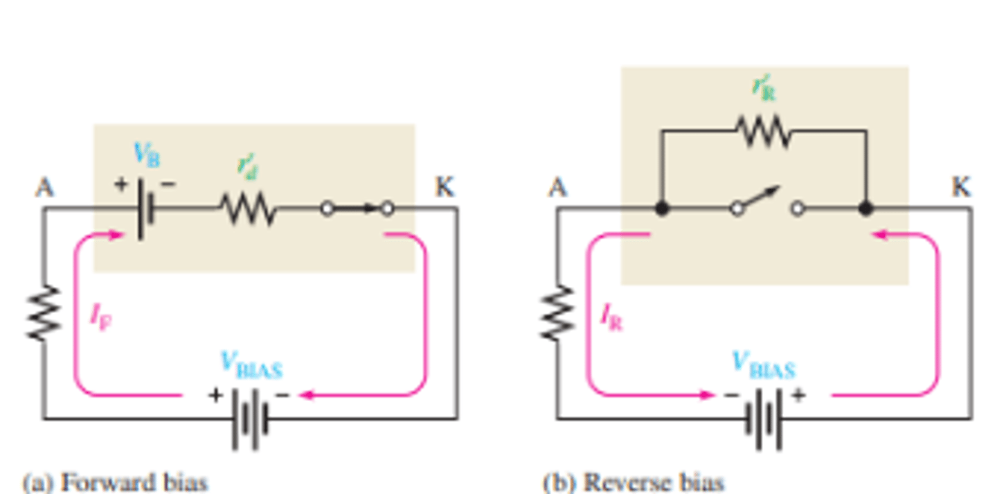
What is the set up for forward bias?
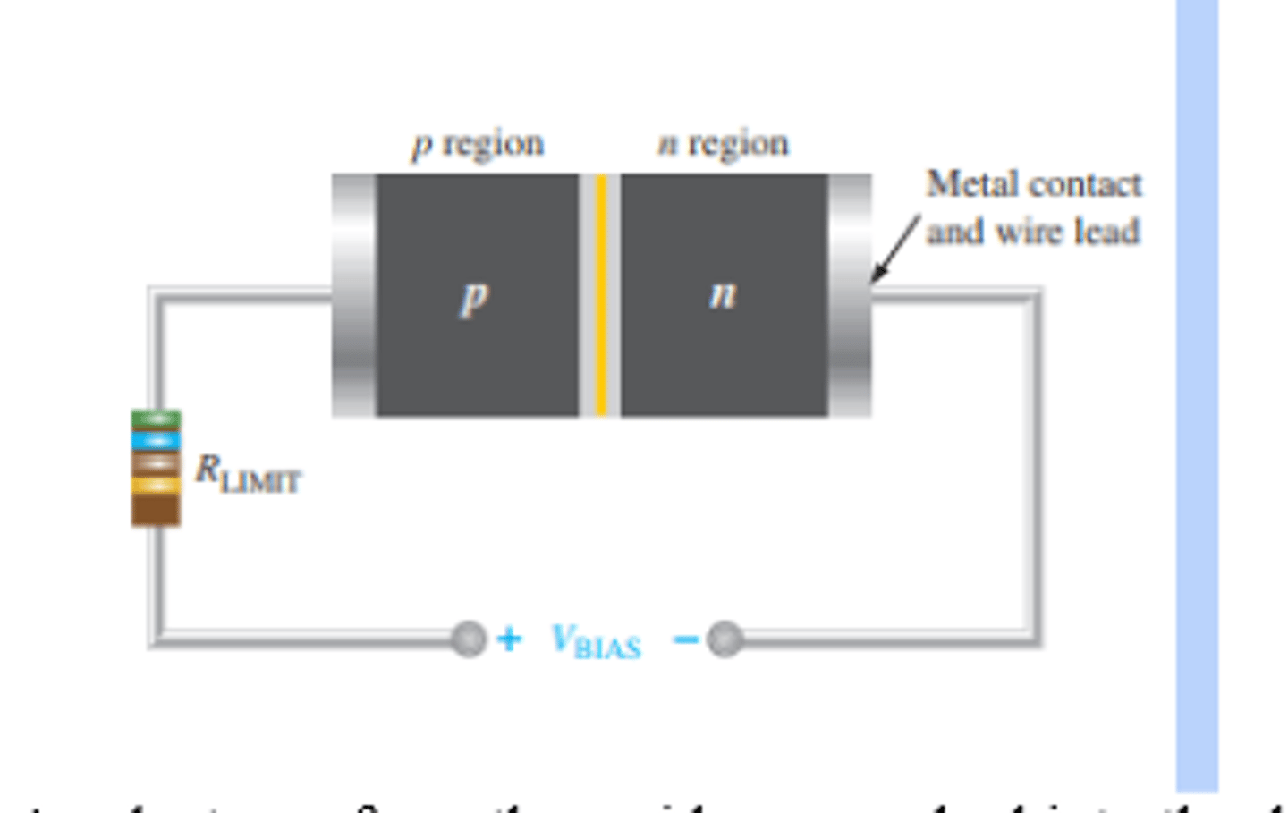
What is forward bias?
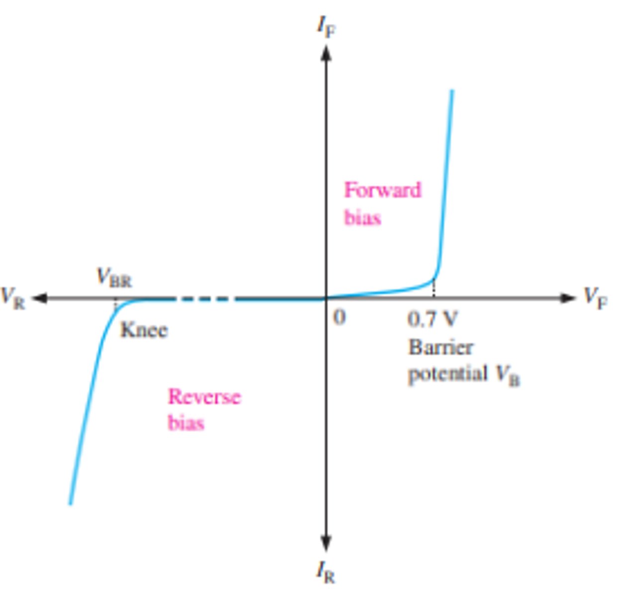
Forward bias is the condition that allows current through the pn junction
How is the barrier potential created, and what's its value for silicon diodes?
As electrons from the n side are pushed into the depletion region, they combine with holes on the p side, reducing the depletion region
This creates the barrier potential, which is approximately 0.7 V
What is the set up for reverse bias?
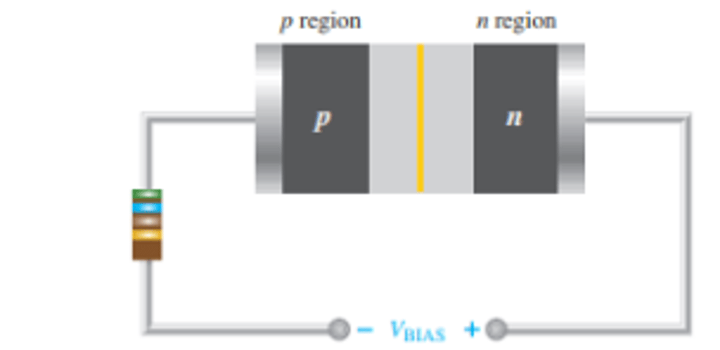
What is reverse bias?
Reverse bias is the condition that essentially prevents current through the diode
What happens at reverse breakdown?
when a diode reaches reverse breakdown, its voltage remains almost constant even though the current changes drastically
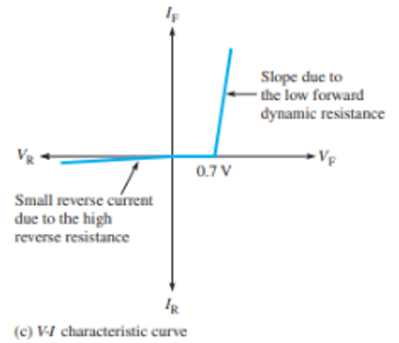
What is the general shape of the V-I characteristic curve for a diode?
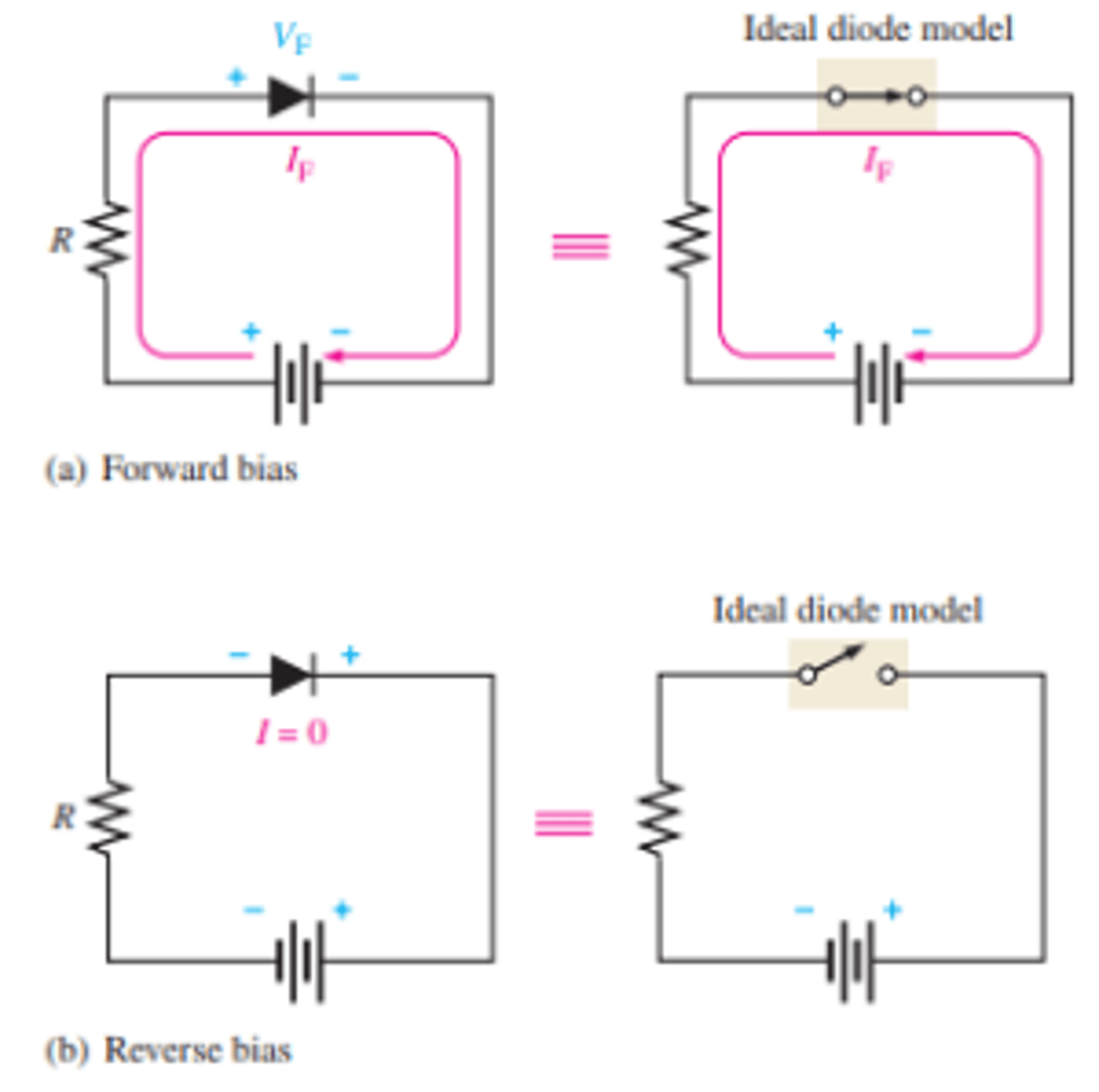
What is the ideal diode model for forward and reverse bias modes?
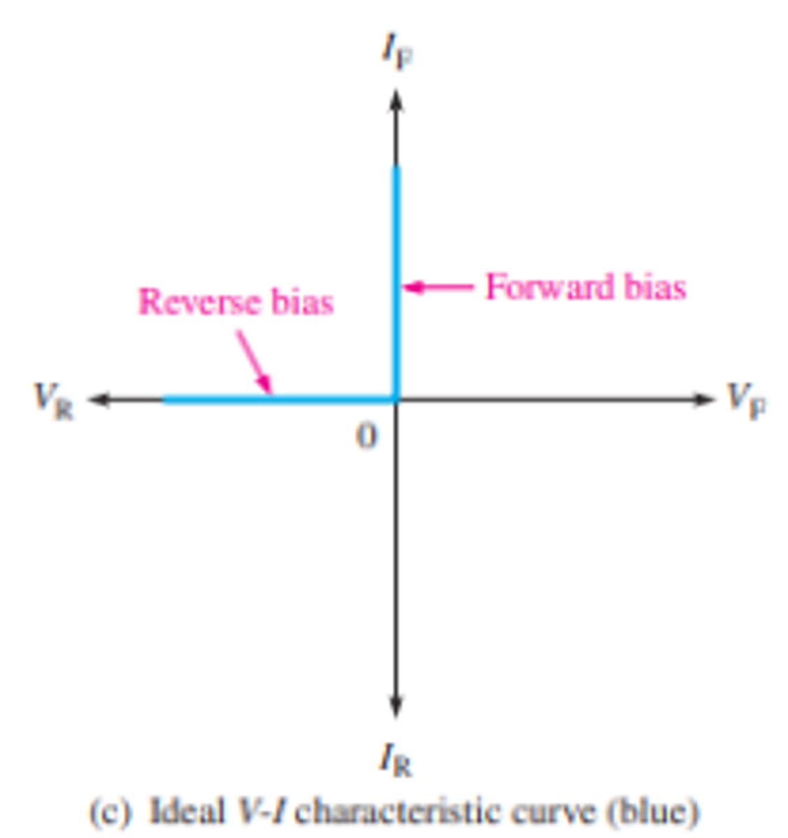
What is the ideal V-I characteristic curve?
What is forward voltage and forward current for the ideal diode model?
VF = 0
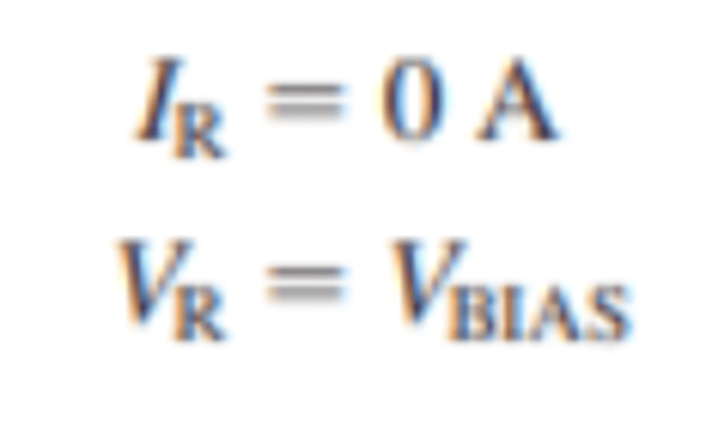
What is reverse voltage and reverse current for the ideal diode model?
IR = 0A
VR = VBIAS
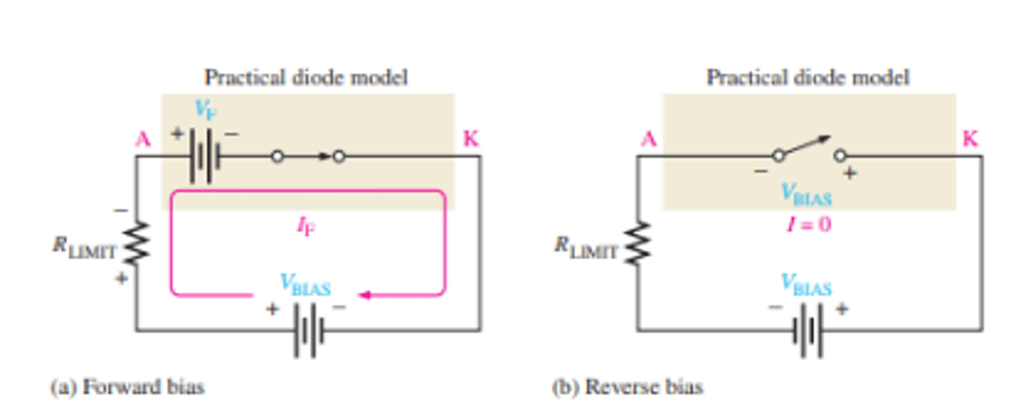
What is the practical diode model in forward and reverse bias modes?
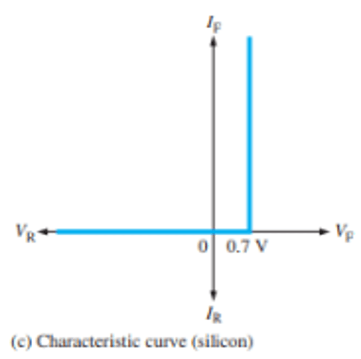
What is the practical characteristic curve for a silicon diode
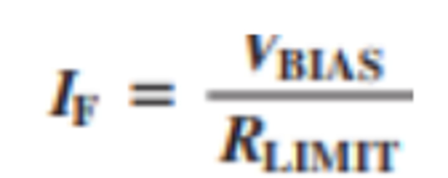
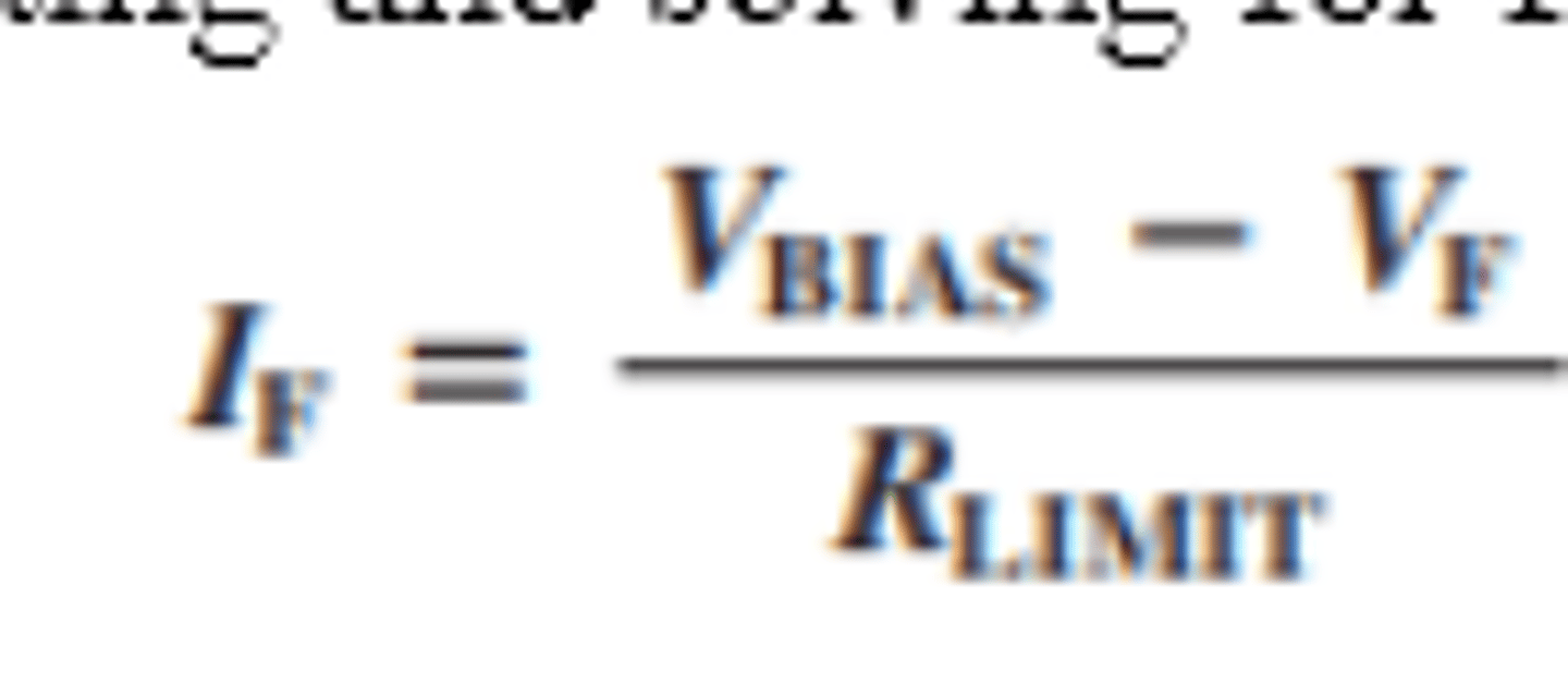
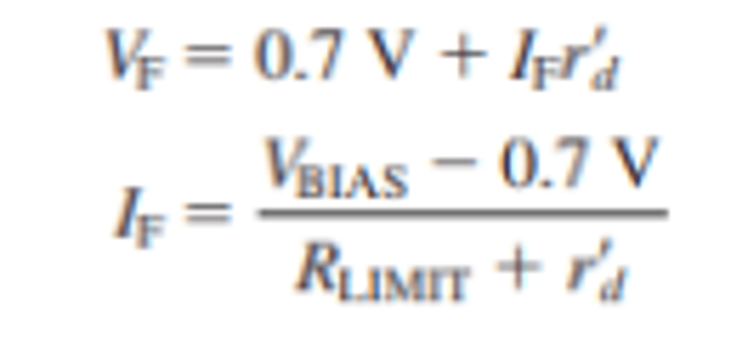
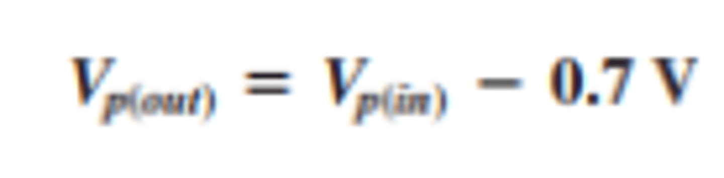
What is the forward voltage and forward current of the practical diode model?
VF = 0.7 V
What is the reverse voltage and reverse current of the practical diode model?
What is the forward and reverse set up for the complete diode model?
What is the V-I curve for the complete diode model?
How is the forward voltage and forward current found for the complete diode model?
What is the setup and output for a half wave rectifier?
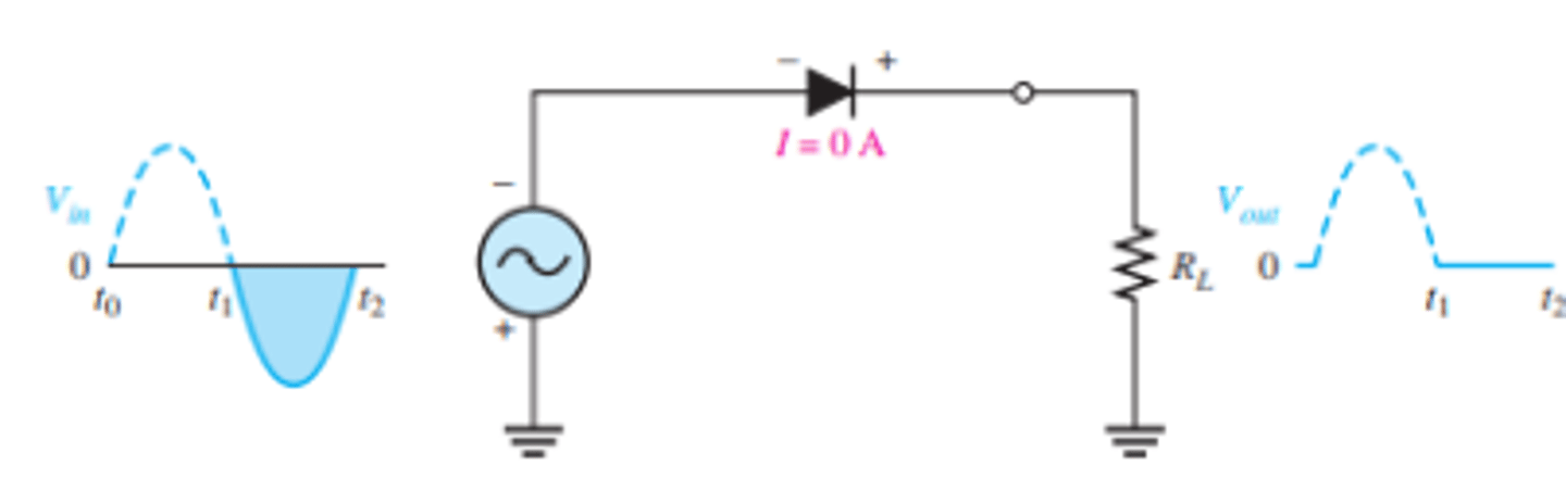
When is the diode in forward and reverse bias for a half wave recitifier?
When the sinusoidal input voltage (Vin) goes positive, the diode is forward-biased
During the negative alternation of the input voltage, the current is 0, so the output voltage is also 0.
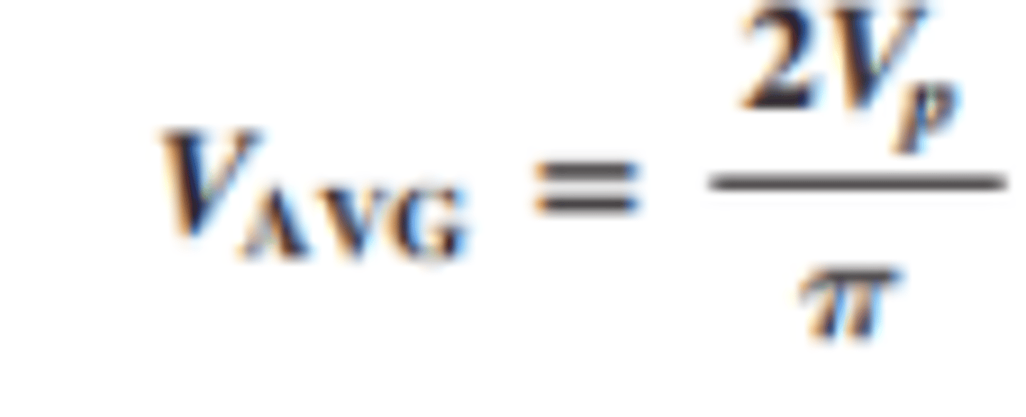
What is the average voltage for a half wave rectifier?
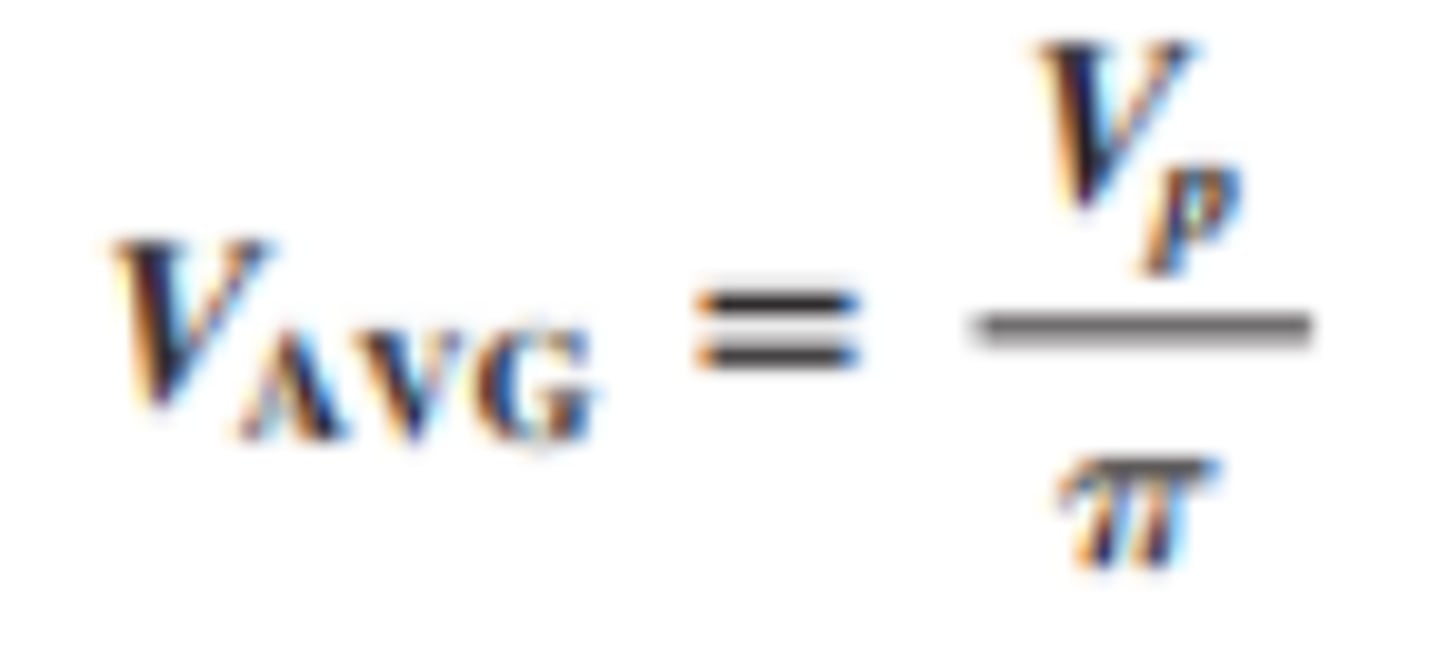
What is the peak output voltage of a halfwave rectifier?
What is the Peak Inverse voltage?
the peak value of the input voltage
What should a diode be rated compared to the PIV
A diode should be rated at least 20% higher than the PIV.
When does the PIV occur?
at the peak of each half-cycle of the input voltage when the diode is reverse-biased.
What is the set up[ for a half-wave rectifier with a transformer coupled input voltage?
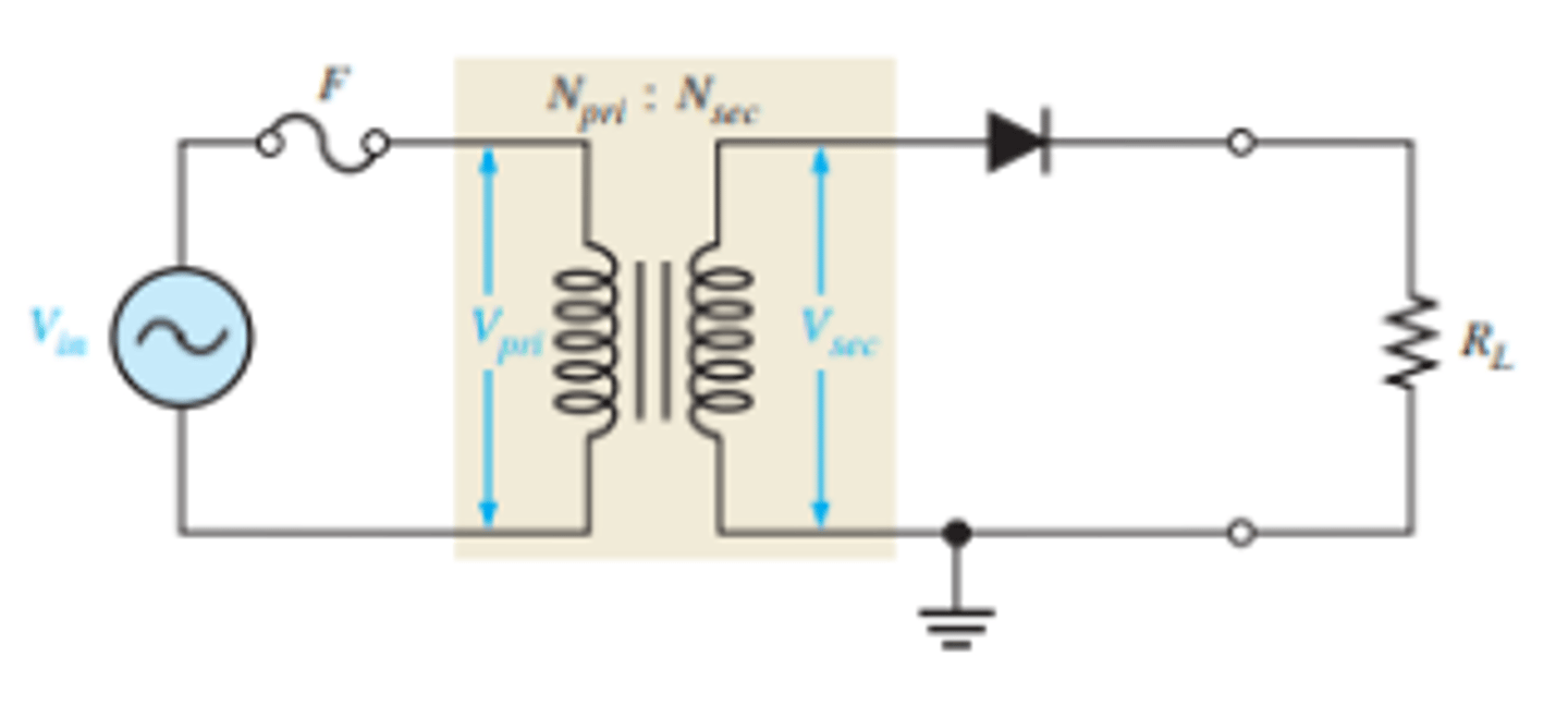
What determines the amount the voltage is changed?
the turns ratio of the transformer
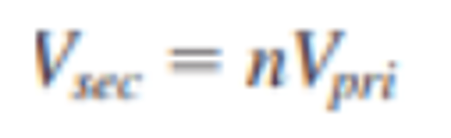
How is the secondary voltage found?
the turns ratio, n, times the primary voltage.
How is peak output voltage found for a half wave rectifier with transformer coupling?
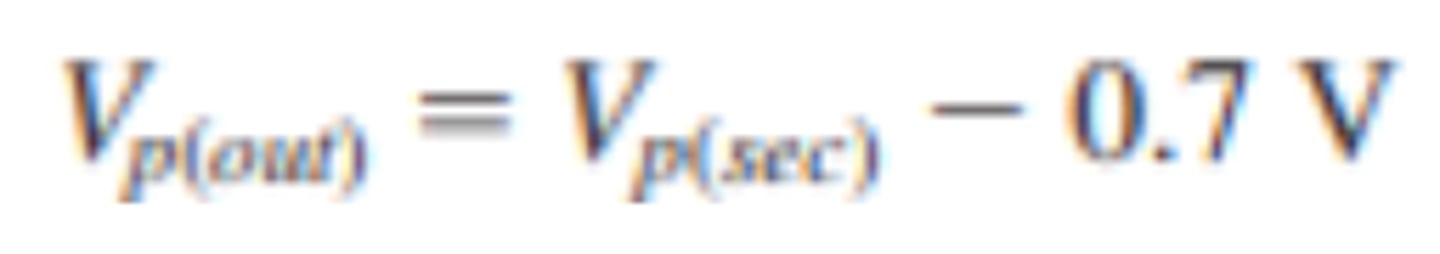
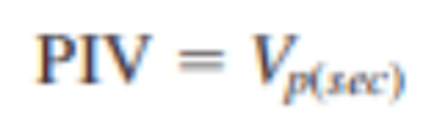
What is the PIV of a half wave rectifier with transformer coupling?
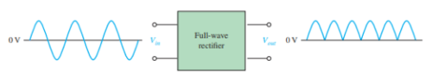
What is the average voltage for a full wave rectifier?
What does the general shape of a full wave rectifier's output wave look like?
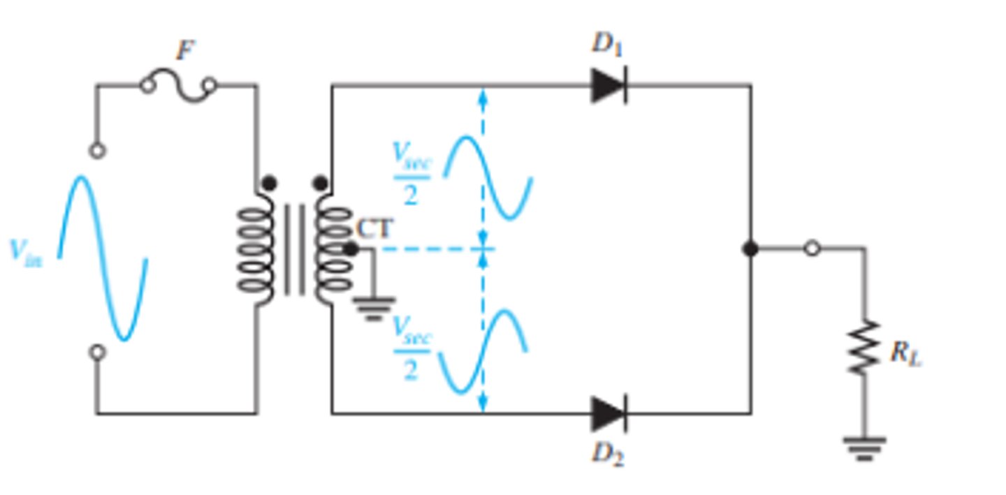
What is the set up for a center-tapped full wave rectifier?
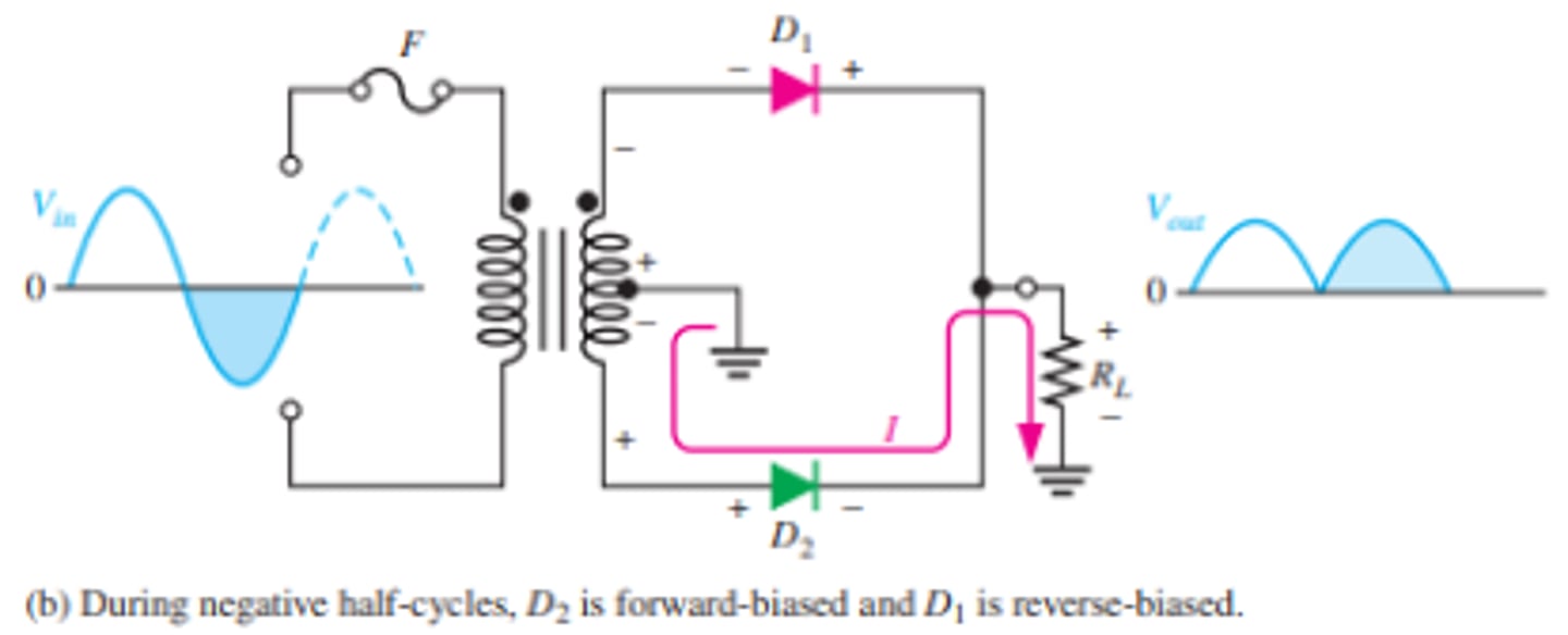
How does a positive half cycle effect a center tapped full wave rectifiers output?
This condition forward-biases diode D1 and reverse-biases diode D2.
How does the negative half cycle of a center tapped full wave rectifier effect the outputs wave?
This condition reverse-biases D1 and forward-biases D2.
What does the setup and output waveform look like for a center tapped full wave rectifier?
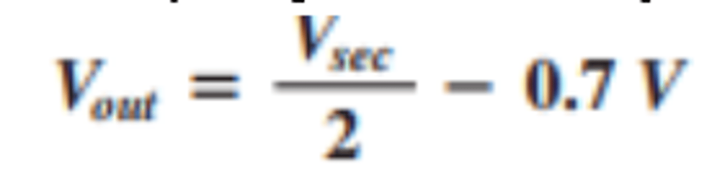
How is the output voltage for a center tapped full wave rectifier calculated?
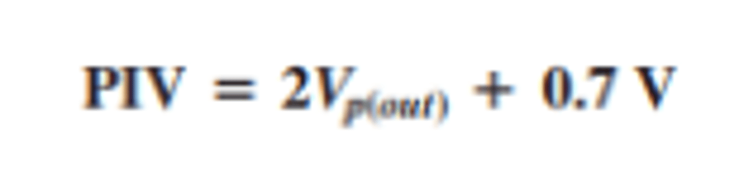
What is the PIV of a center tapped full bridge rectifier?
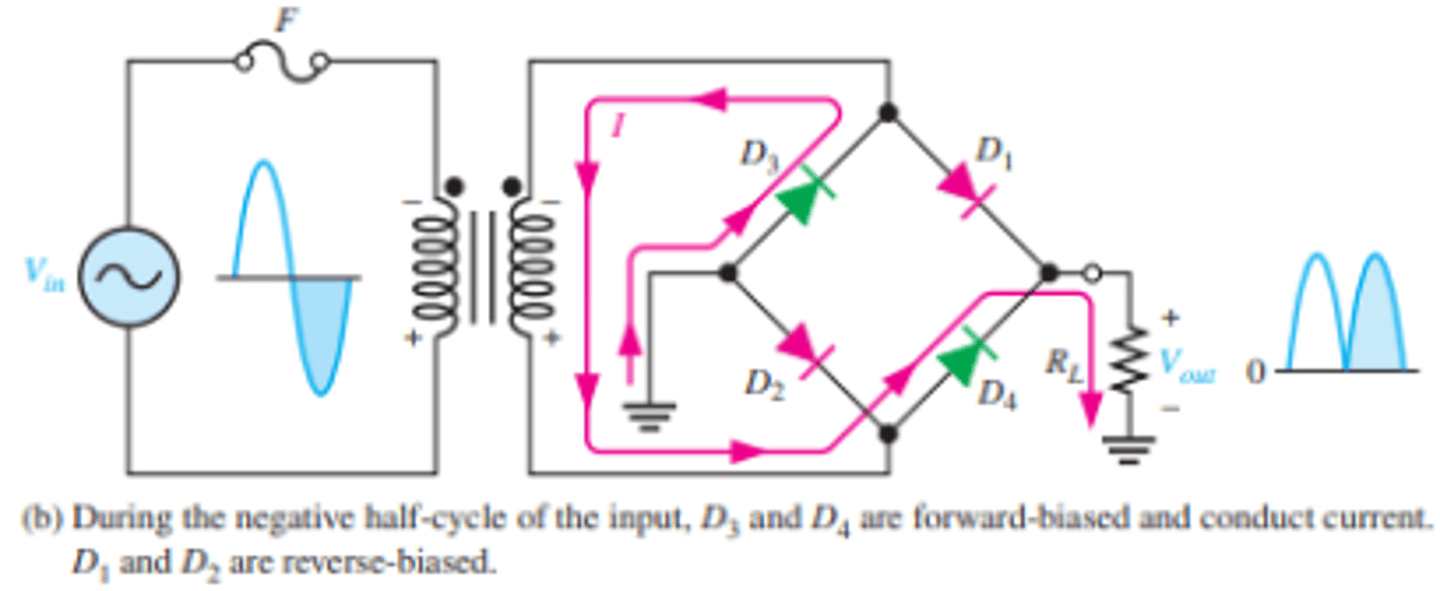
What does the setup and output waveform look like for a bridge full wave rectifier?
How does the positive half cycle for a bridge full wave rectifier effect the biasing of the diodes?
D1 and D2 are forward-biased
D3 and D4 are reverse-biased.
how does the negative half cycle for a bridge full waver rectifier effect the biasing of the diodes?
D3 and D4 are forward biased
D1 and D2 are reverse-biased.
How is the peak output voltage for a bridge full wave rectifier calculated?
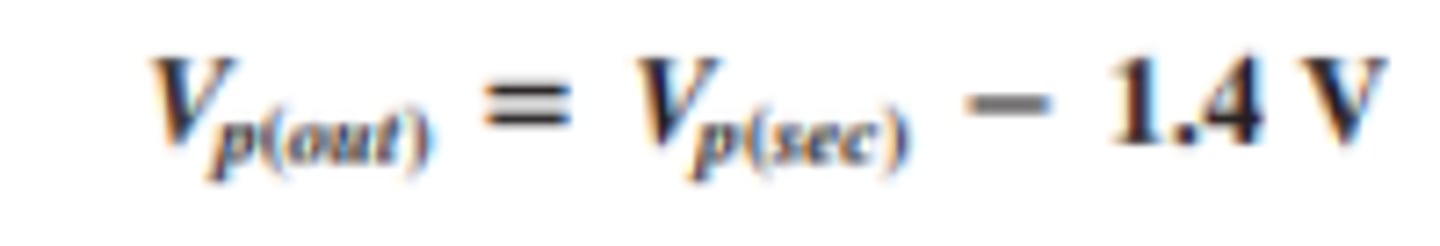
What is the PIV of a bridge full wave recitifer?
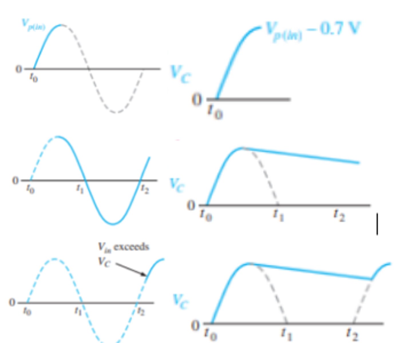
What is the setup for a capacitor-input filter?
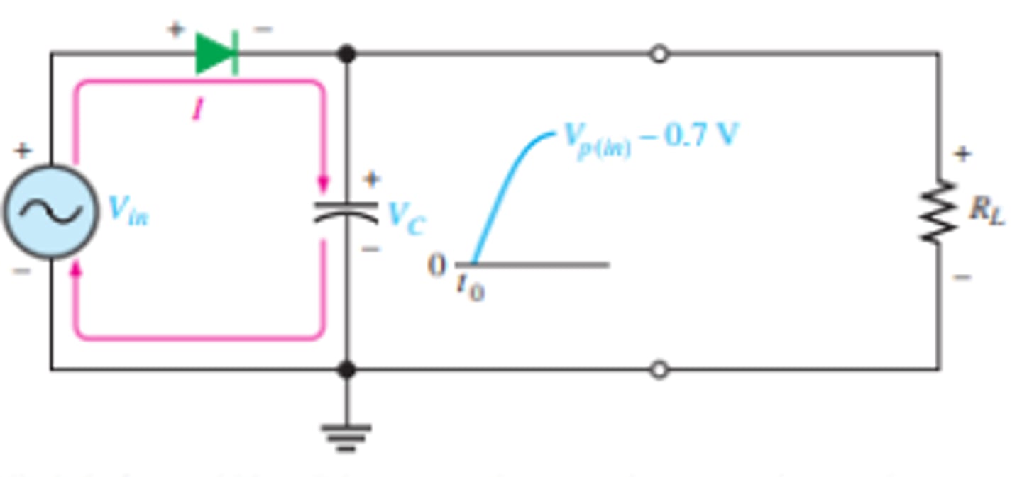
How does the charging of the capacitor effect a capacitor input filter?
Initial charging makes the diode forward bias (only once)
After peak positive half cycle, diode becomes reverse bias as the capacitor discharges
Capacitor charges back to peak of input when diode becomes forward bias.
What does the waveform look like for the output of a capacitor input filter?
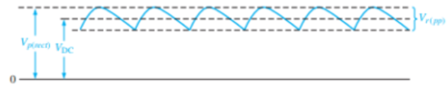
What is ripple voltage?
The variation in the capacitor voltage due to the charging and discharging
What does the ripple voltage show?
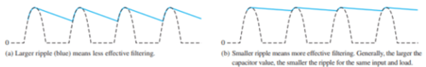
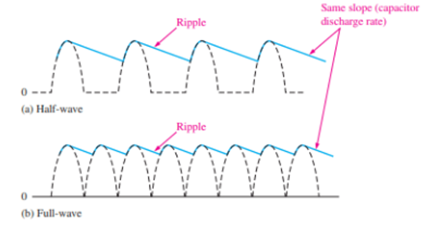
What does the output waveform ripple look like for both full wave and half wave rectified voltages with the same filter capacitor, load, and input.
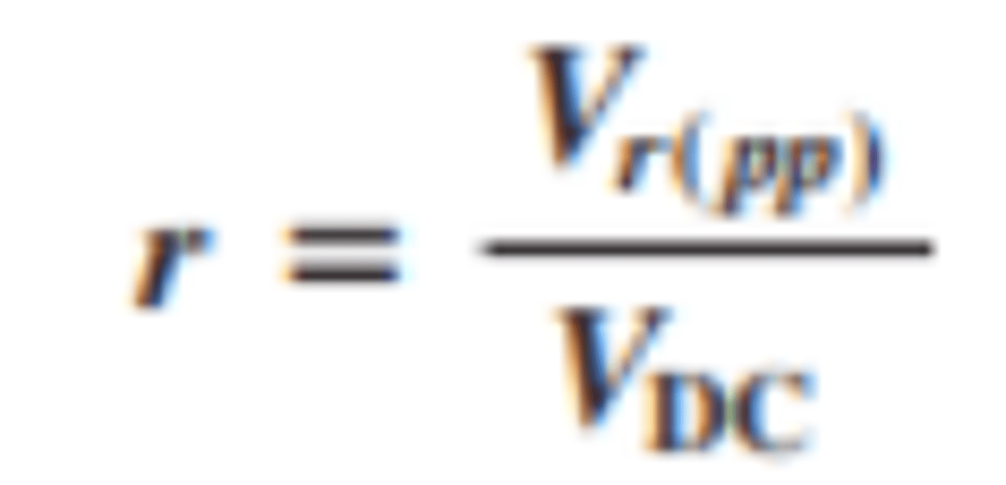
What does the ripple factor show?
an indication of the effectiveness of the filter and is defined as
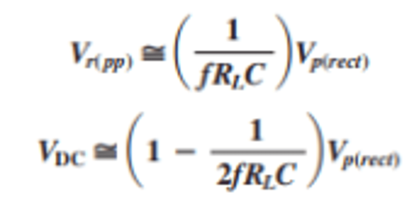
How is ripple factor calcualted?
How are the V_DC, V_p(rect), and V_r(pp) shown on a ripple?
How is peak to peak ripple voltage and DC voltage found for a full wave rectifier with a capacitor input filter?
The variable Vp(rect) is the unfiltered peak rectified voltage
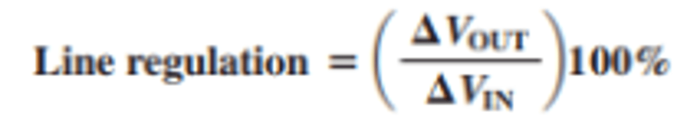
What is line regulation, and hows it found?
line regulation specifies how much change occurs in the output voltage for a given change in the input voltage.
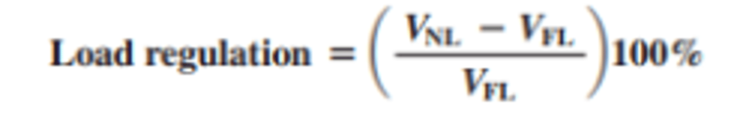
What is load regulation and how is it found?
load regulation specifies how much change occurs in the output voltage over a certain range of load current values, usually from minimum current (no load, NL) to maximum current (full load, FL).
What are diode limiters?
a diode limiter (also called clipper) that limits or clips the positive part of the input voltage.
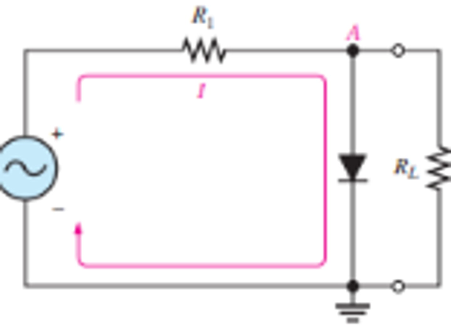
What is the set up for a positive clipper circuit?
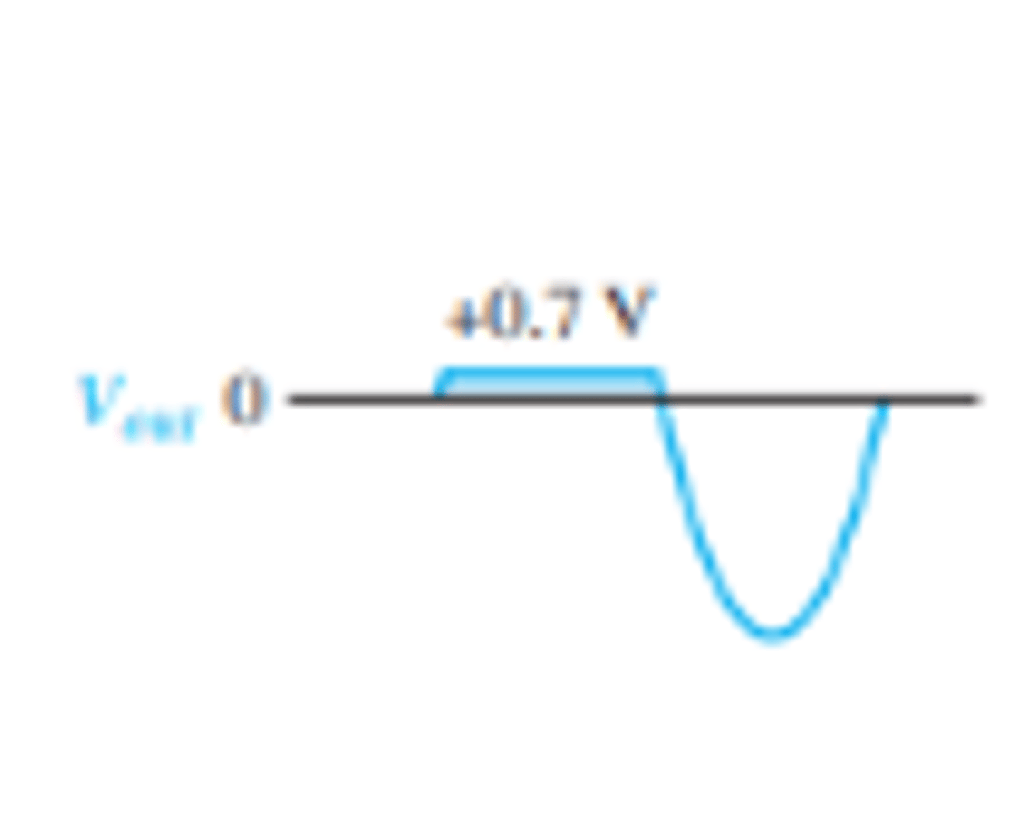
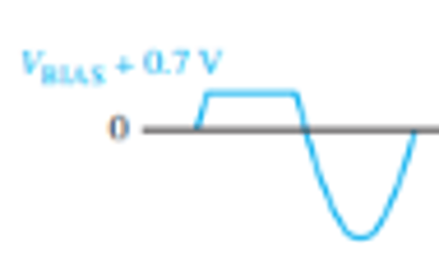
What does the output waveform look like for a positive clipper circuit?
Forward bias for positive half cycle above 0.7 V and reverse during negative half cycle
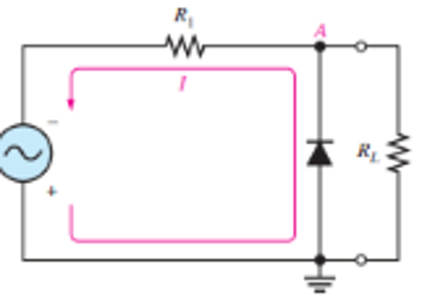
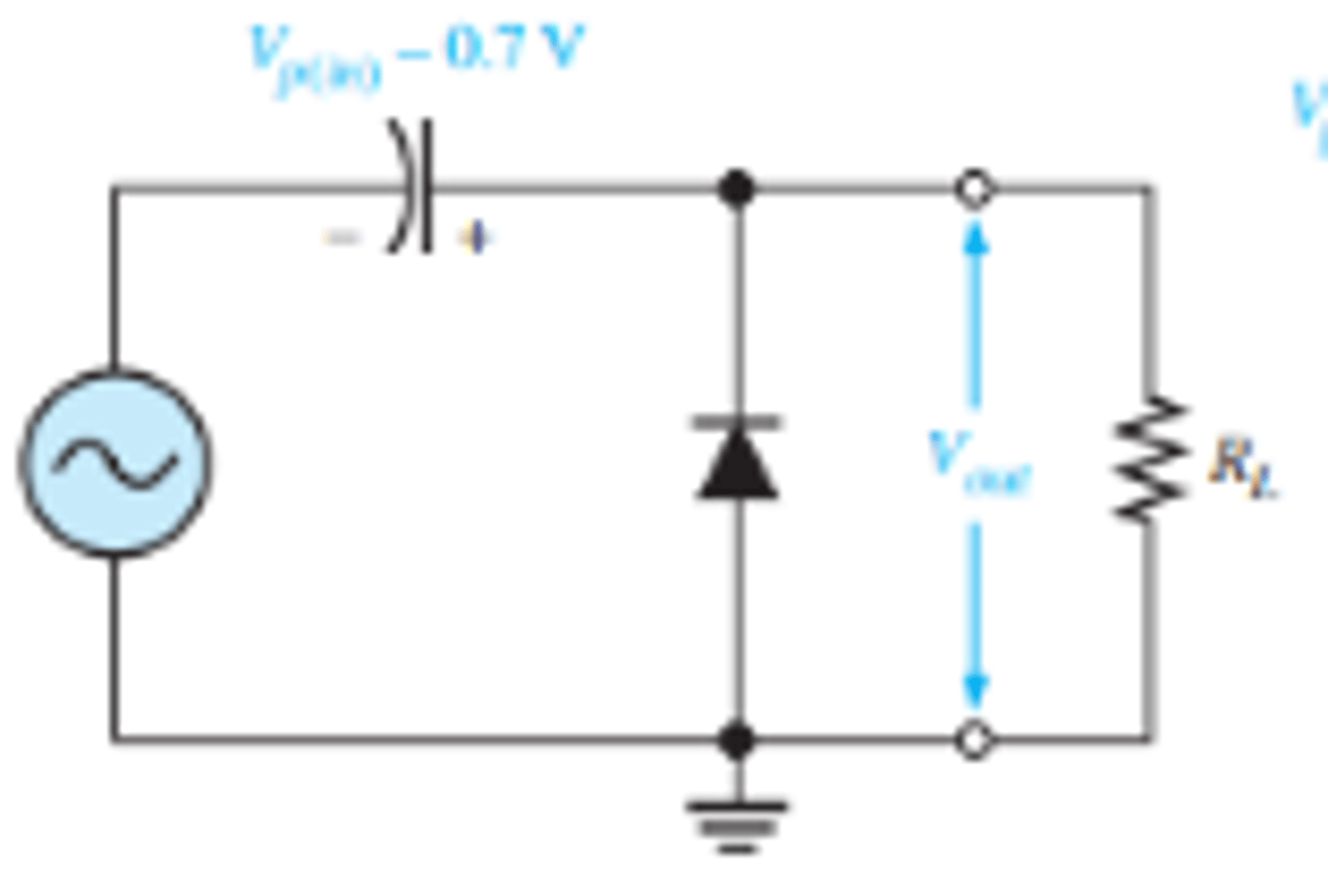
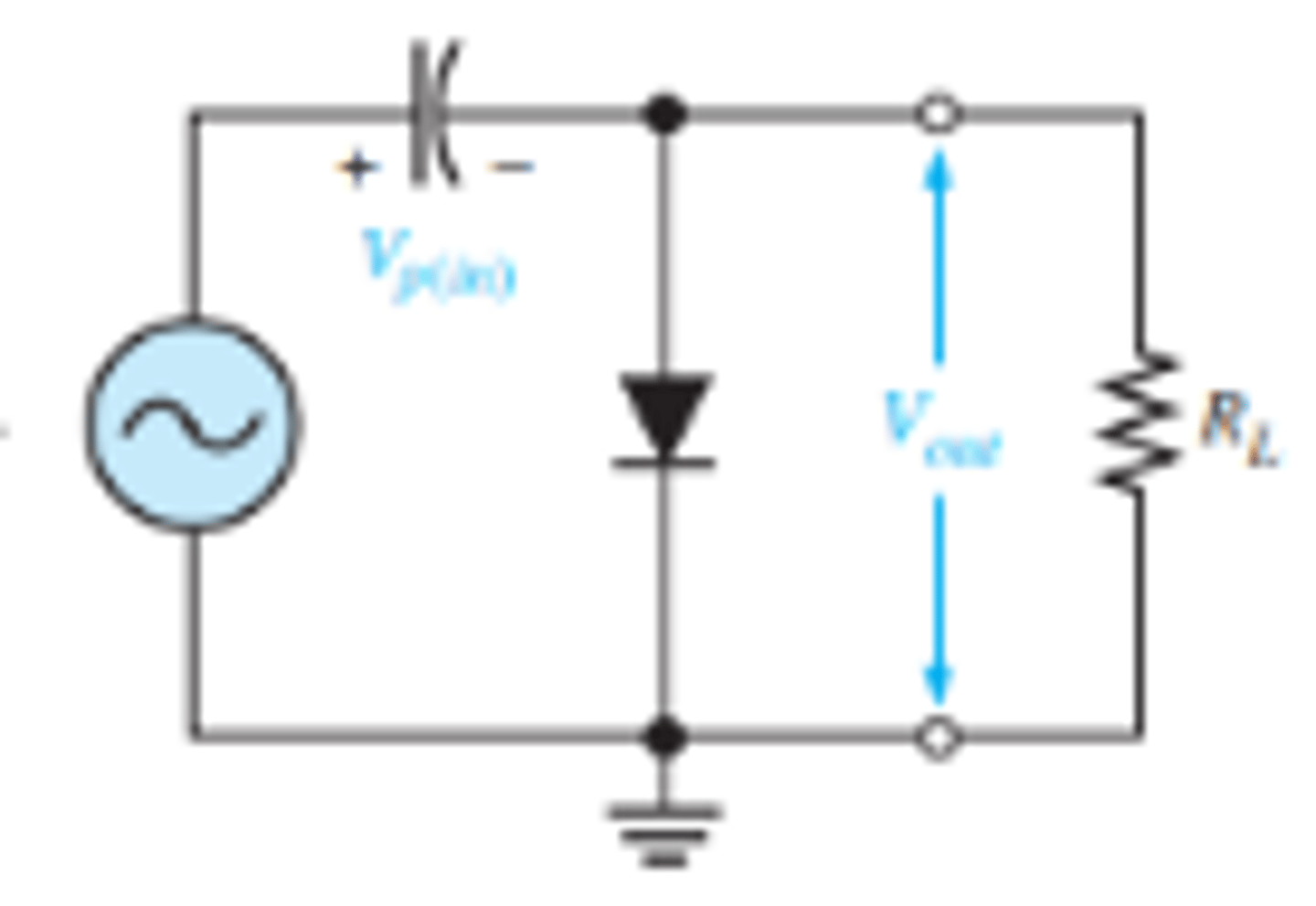
What is the set up for a negative clipper circuit?
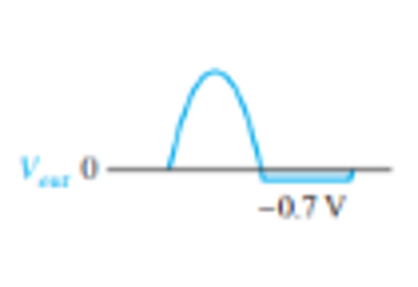
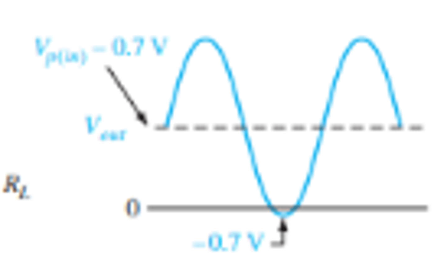
What does the output waveform look like for a negative clipper circuit?
Reverse bias during positive half cycle and forward during negative half cycle below 0.7 V
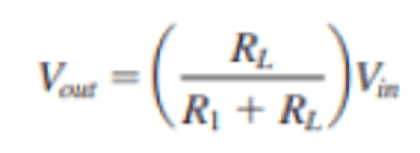
How is output voltage calculated for a clipper circuit?
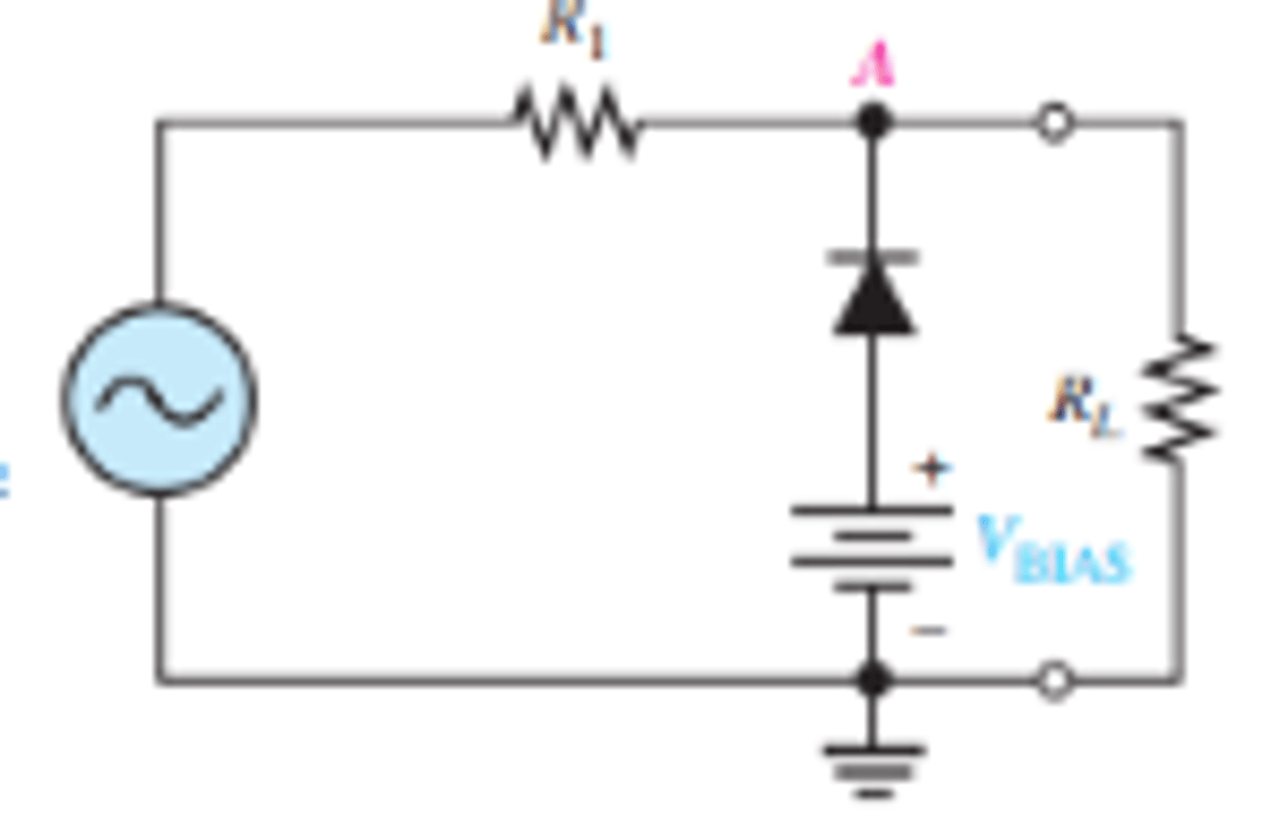
What is the setup for a biased positive clipper circuit?
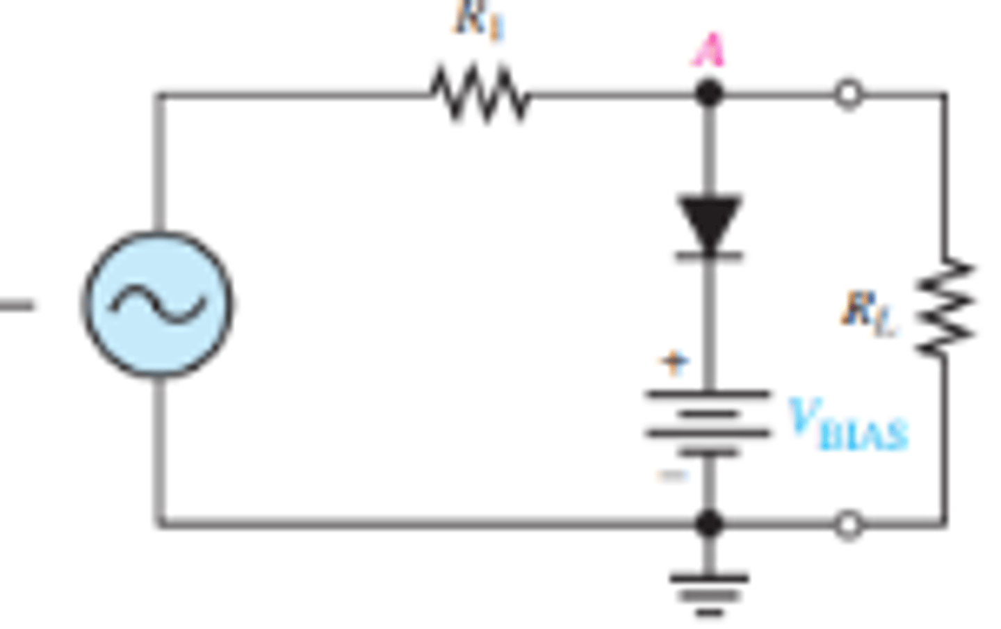
How is the output voltage effected when a positive clipper circuit is biased?
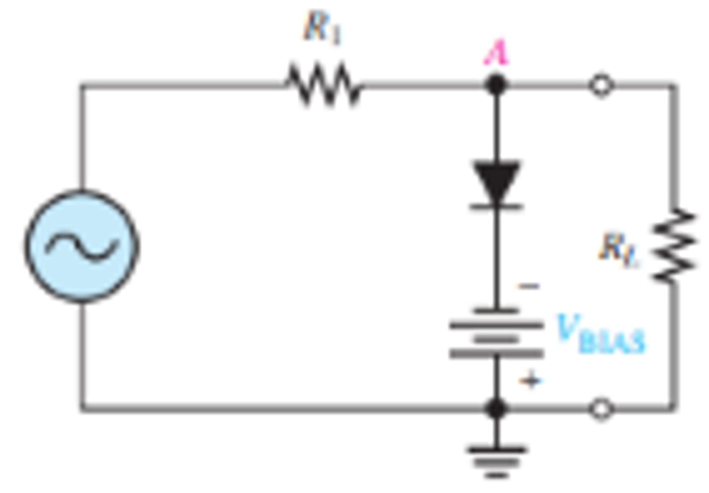
What is the setup for a biased negative clipper circuit?
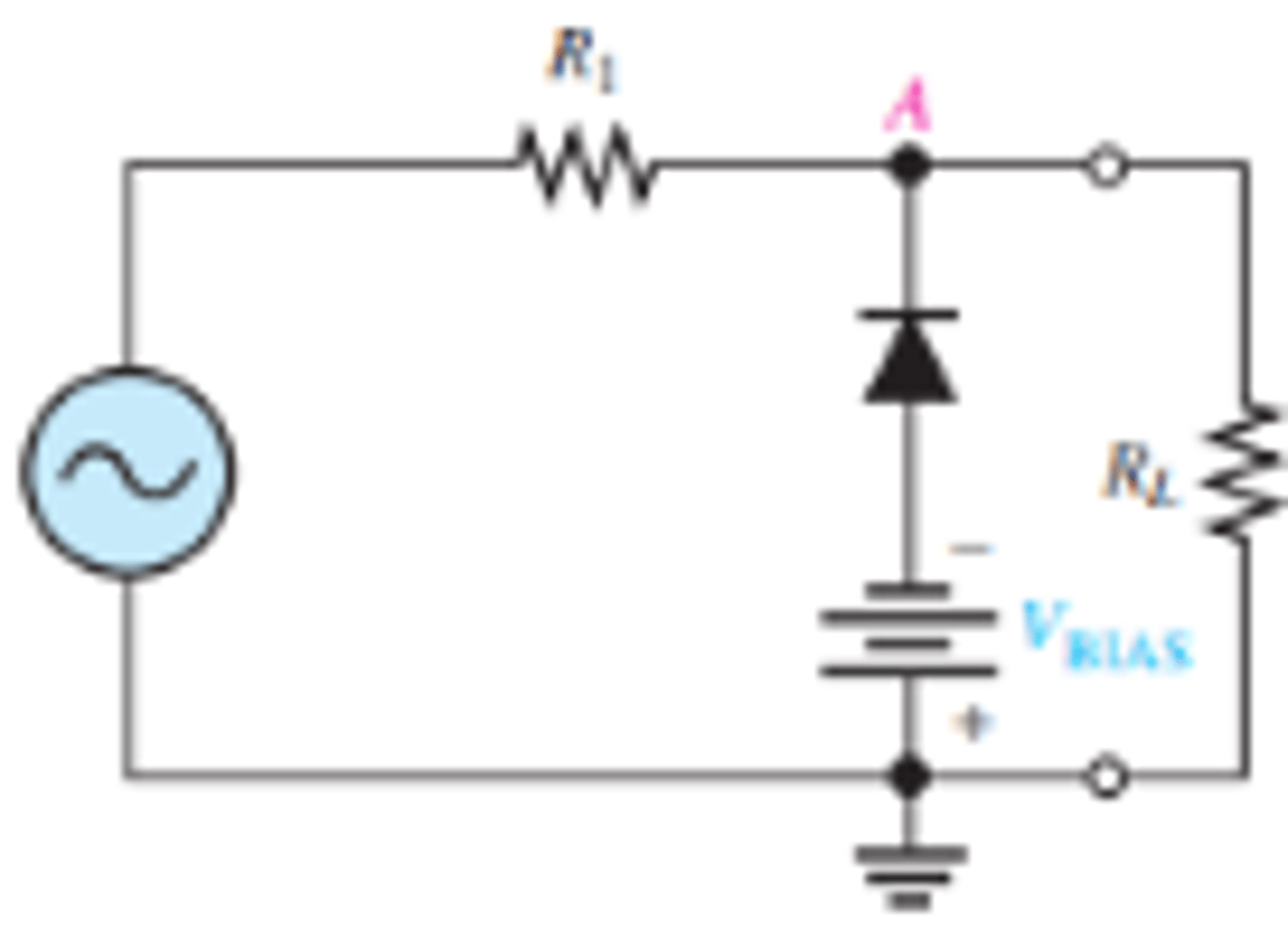
How is the output voltage effected when a negative clipper circuit is biased?
What can be changed in a biased limiter to output voltages above or below a portion of the input?
By turning the diode around, the positive limiter can be modified to limit the output voltage to the portion of the input voltage waveform above VBIAS - 0.7 V, and the negative limiter below -VBIAS + 0.7 V
How does flipping the diode around for a positive clipper effect the output waveform?
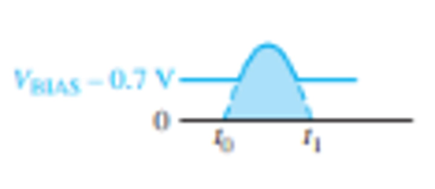
What is the setup for a positive biased clipper that limits output to a portion above the input waveform?
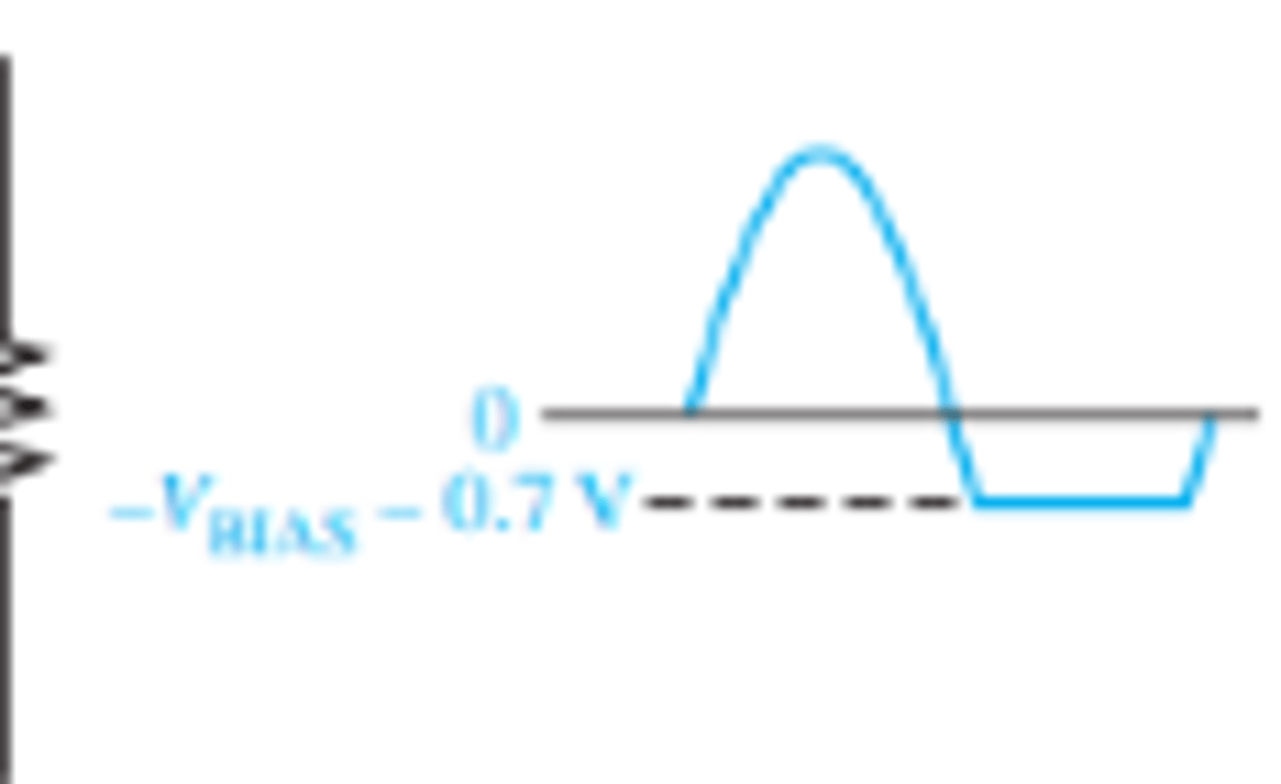
How does flipping the diode around for a negative clipper effect the output waveform?
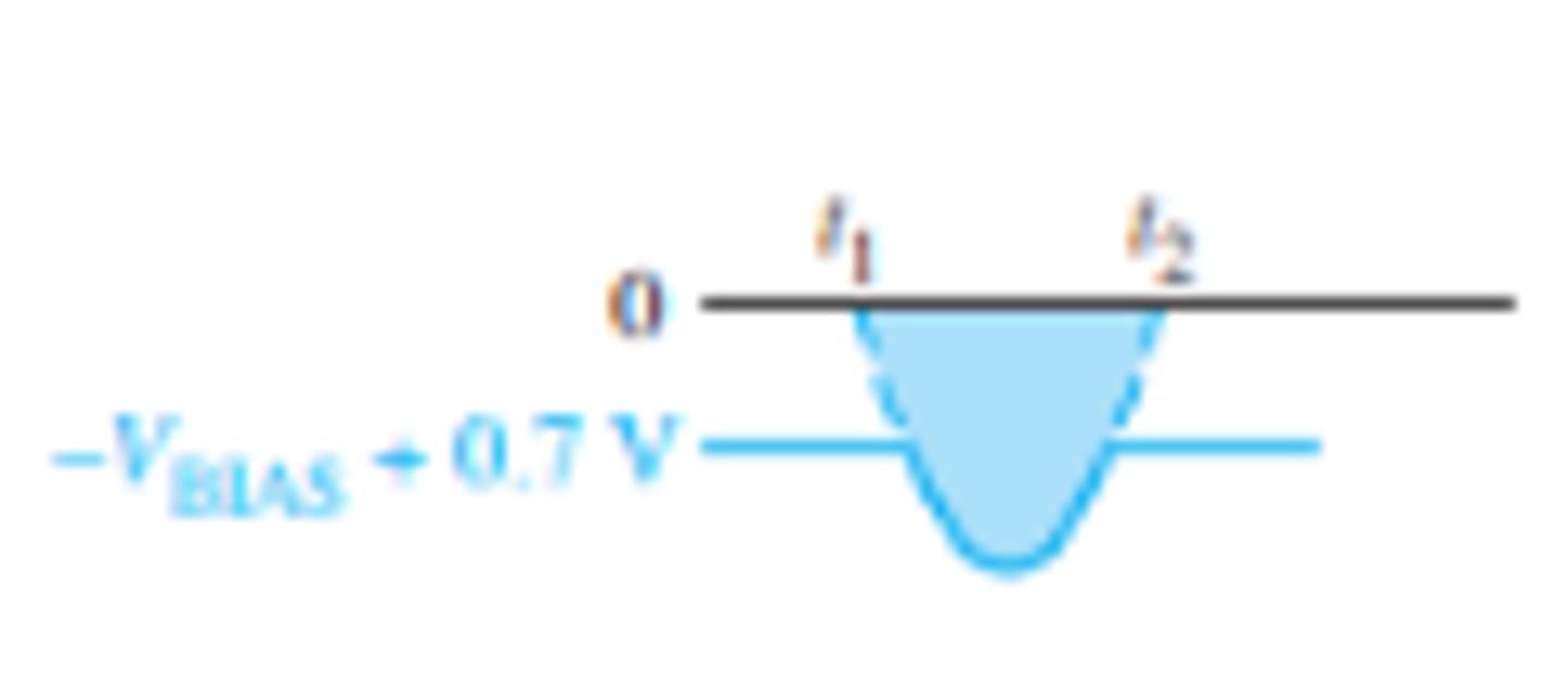
What is the setup for a negative biased clipper that limits output to a portion below the input waveform?
What are diode clampers?
A clamper adds a dc level to an ac voltage.
Clampers are sometimes known as dc restorers.
How does a diode clamper effect the outputs waveform?
BY shifting the waveform to a 99% above or below the x-axis. Leaving 0.7 V extending past the x-axis.
What is the setup for a diode clamper that shifts the output waveform mostly above the X-Axis?
What is the setup for a diode clamper that shifts the output waveform mostly below the X-Axis?
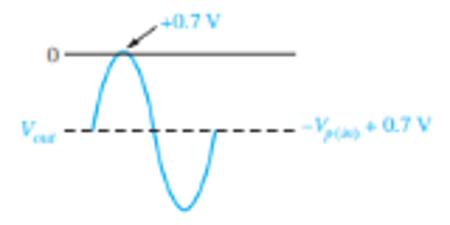
What does the waveform look like for a positively shifted output on a diode clamper?
What does the waveform look like for a negatively shifted output on a diode clamper?
What is a voltage doubler circuit?
A voltage doubler is a voltage multiplier with a multiplication factor of two
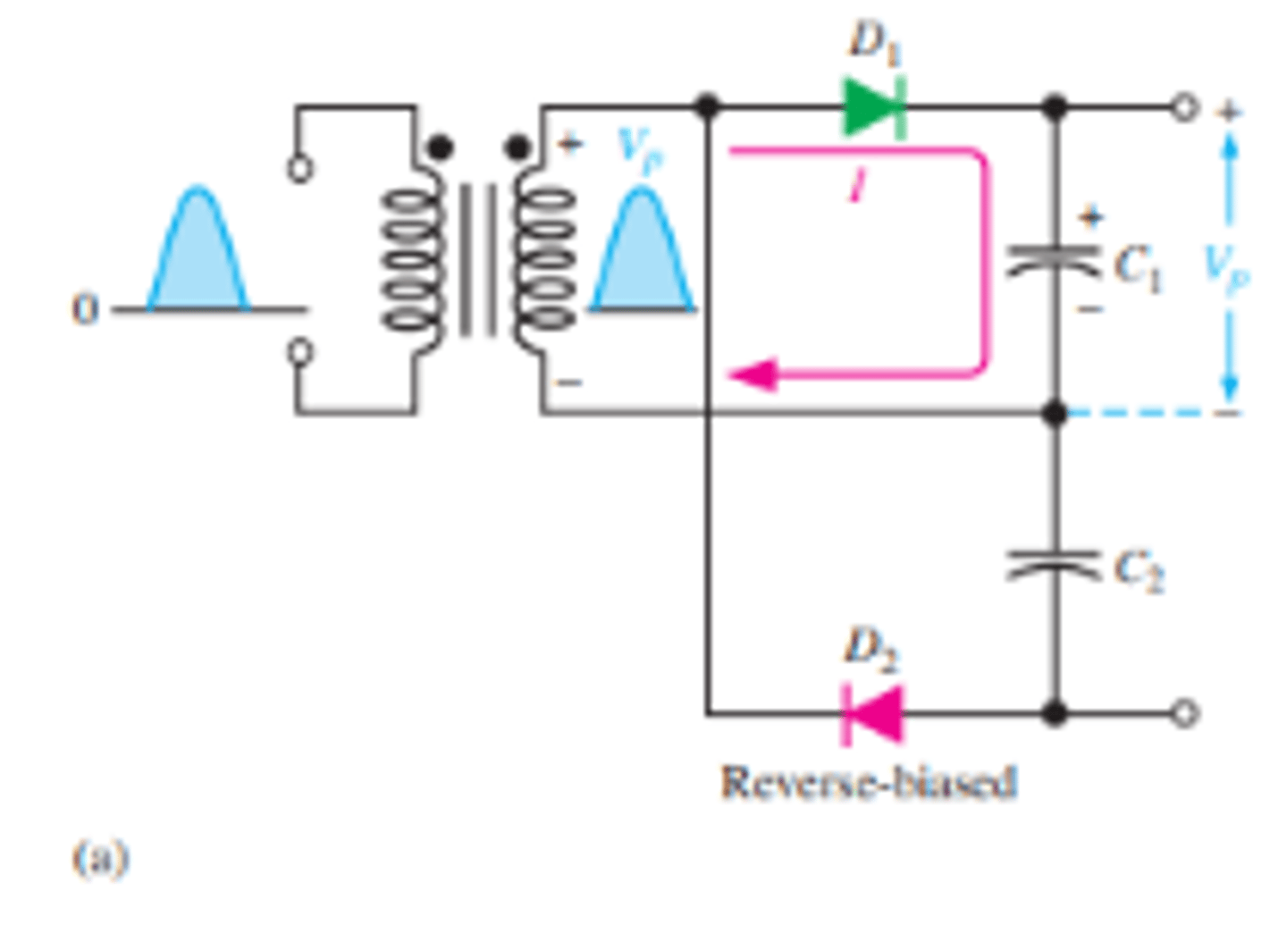
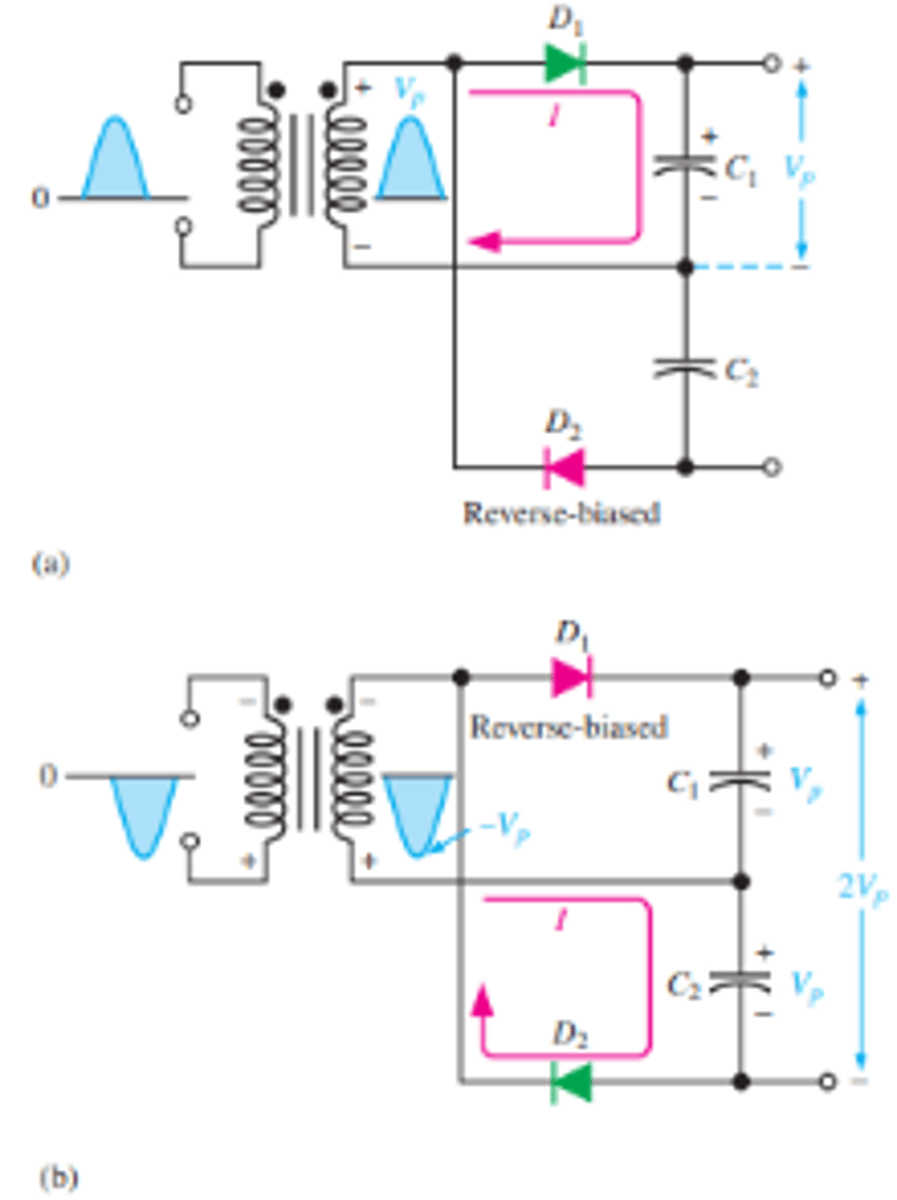
What is the setup for a half wave voltage doubler?
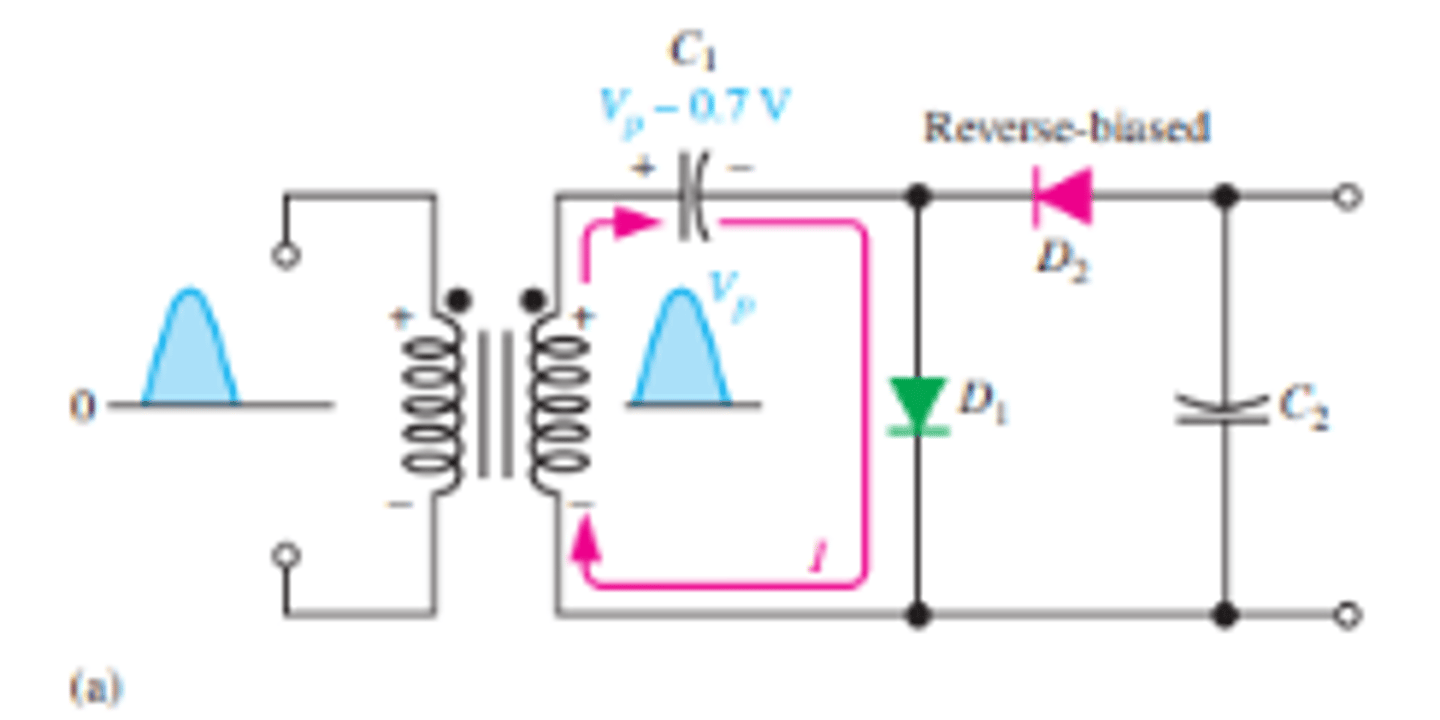
What is the biasing of the diodes for a half wave voltage doubler during the positive and negative half cycles?
During the positive half-cycle of the secondary voltage, diode D1 is forward-biased and D2 is reverse biased
During the negative half-cycle, diode D2 is forward biased and D1 is reverse-biased
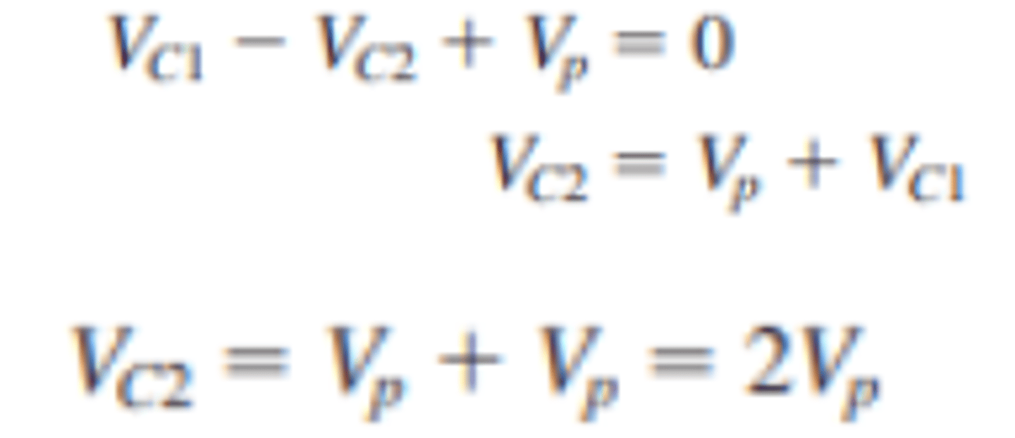
How is the voltage across the capacitors in a half wave voltage doubler circuit calculated?
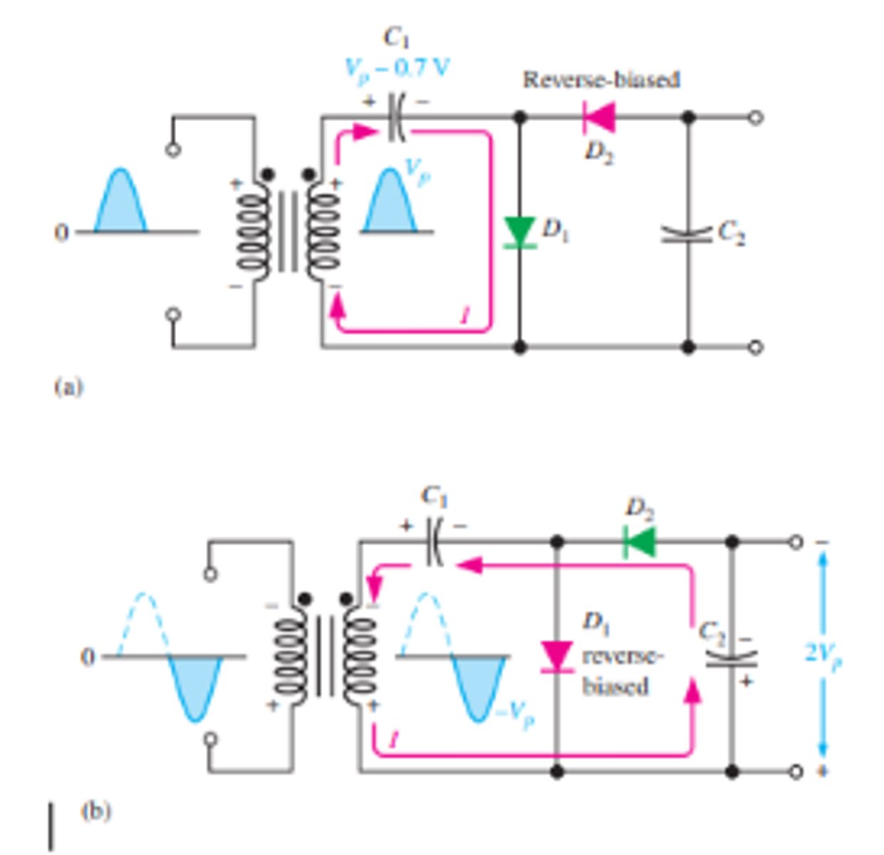
What is the setup for a full wave voltage doubler circuit?
What is the biasing of the diodes during the positive and negative half cycles for a full wave voltage doubler?
When the secondary voltage is positive, D1 is forward-biased and C1 charges to approximately Vp
During the negative half-cycle, D2 is forward-biased and C2 charges to approximately Vp
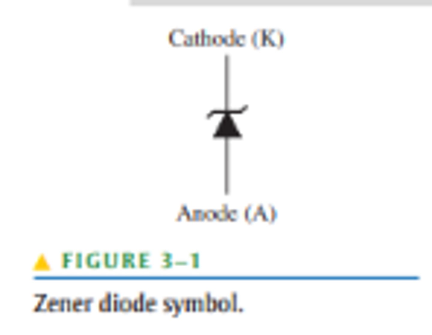
What is a Zener diode?
A zener diode is a silicon pn junction device that is designed for operation in the reverse-breakdown region.
What does a zener diode symbol look like?
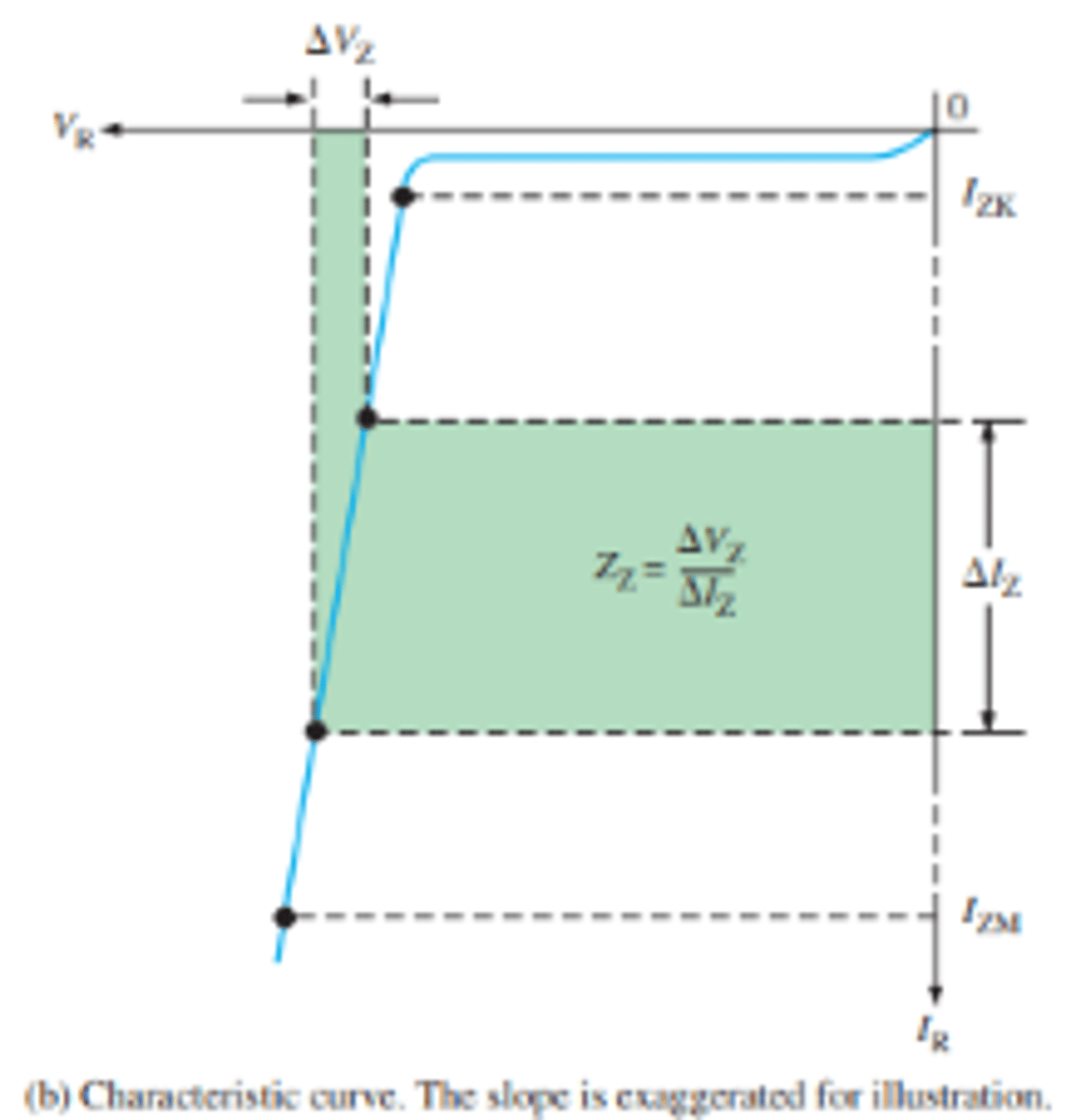
What is the general Zener diode V-I characteristic curve?
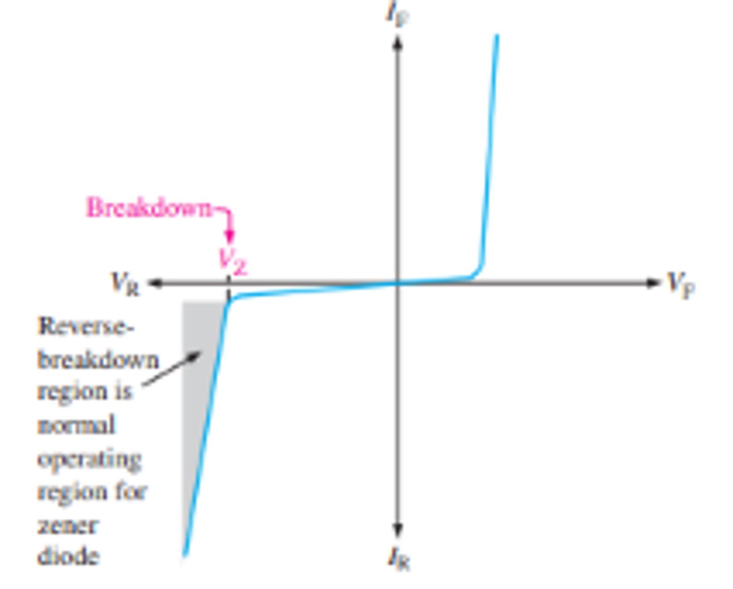
What are the two types of zener breakdown?
(1) avalanche effect, occurs in both rectifier and zener diodes at a sufficiently high reverse voltage.
(2) Zener breakdown occurs in a zener diode at low reverse voltages
What is the general rule for categorizing the reverse breakdown operations for a zener diode?
Zener diodes with breakdown voltages of less than approximately 5 V operate predominantly in zener breakdown.
Those with breakdown voltages greater than approximately 5 V operate predominantly in avalanche breakdown.
What is I_ZK and I_ZM and why are they important?
zener diode maintains a nearly constant voltage across its terminals for values of reverse current ranging from the absolute minimum reverse current (IZK) to maximum reverse current (IZM).
What is the practical model for the Zener equivalent circuit?
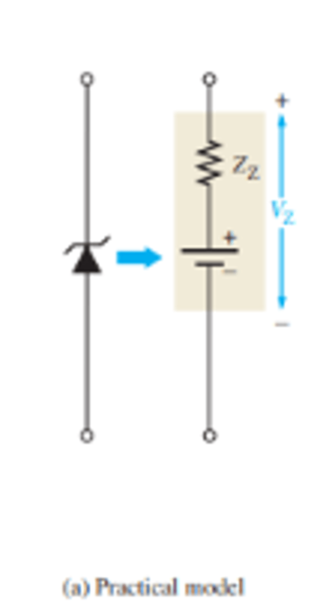
What is V_Z and I_Z and how do they relate?
VZ is measured at the specified zener test current, IZ
What is Z_Z and how is it found and calculated?
ZZ is the maximum zener impedance at the specified test current, IZ.
What is the problem with zener diode regulators, and how is this accounted for?
can provide a reasonably constant dc level at the output, but they are not particularly efficient.
For this reason, they are limited to applications that require only low current to the load.
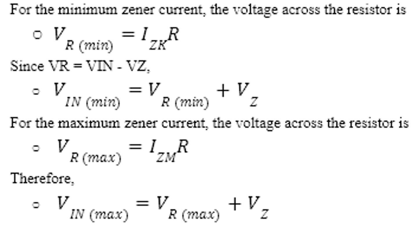
How is minimum and maximum input voltage calculated for zener regulation with a variable input voltage?
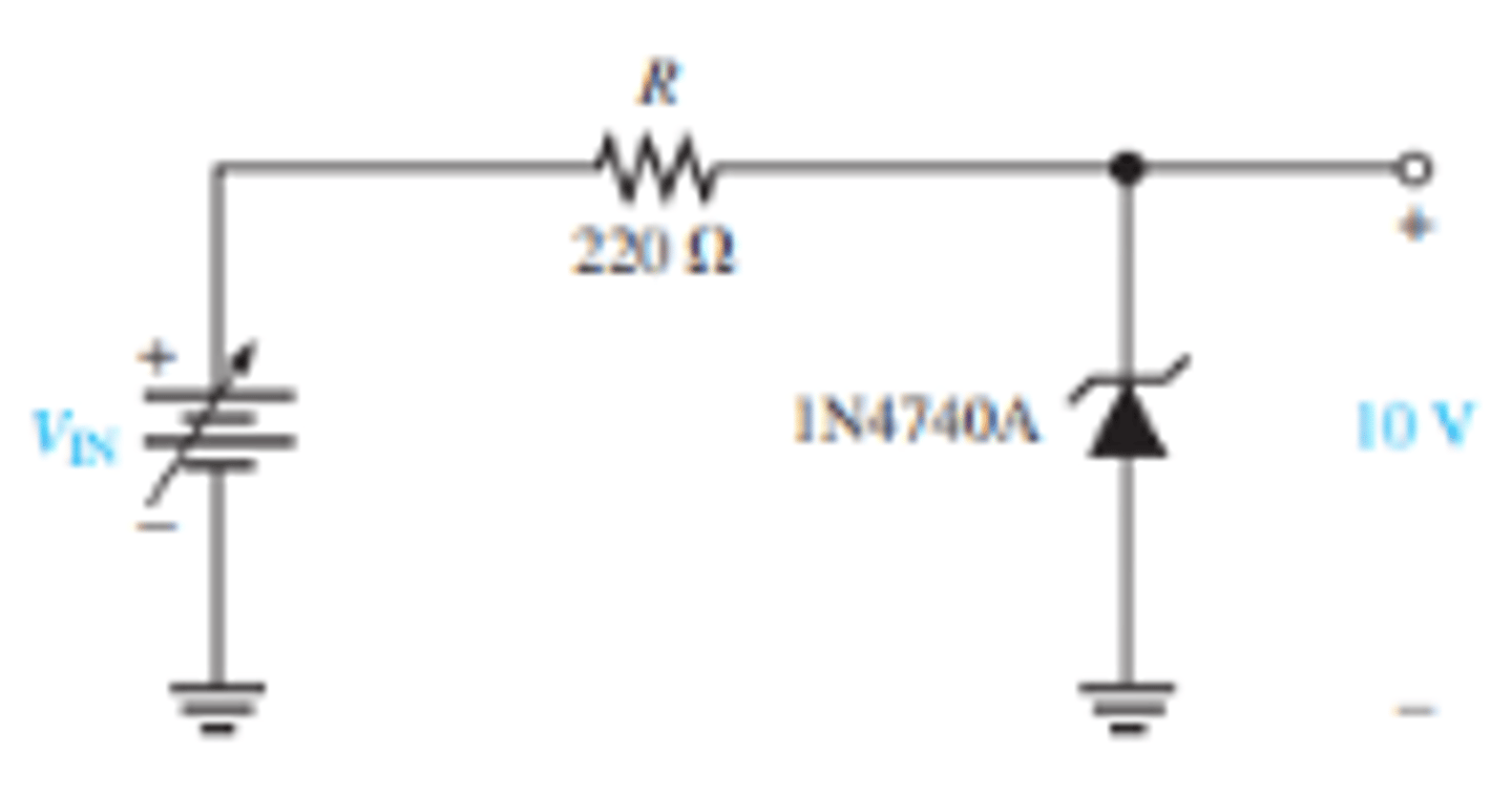
what is the setup for zener regulation with a variable input voltage?
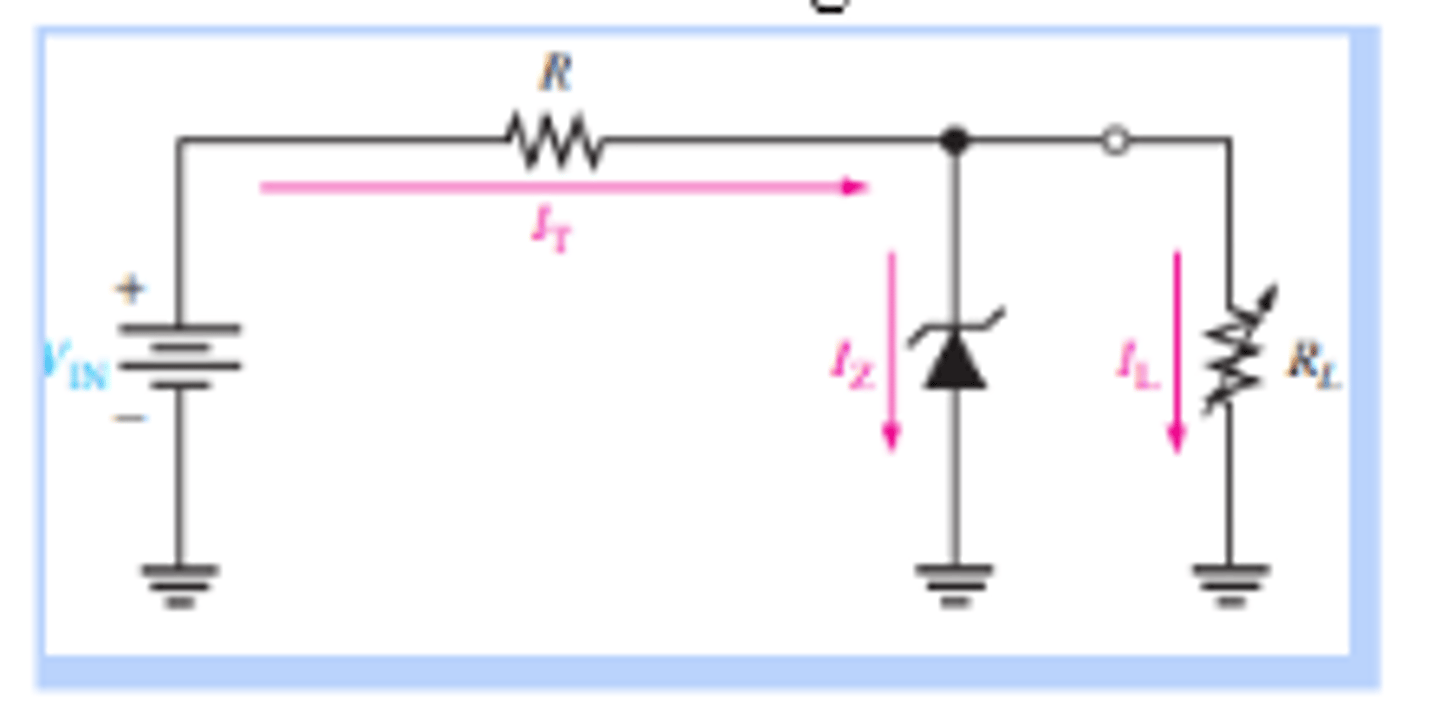
What is the setup for a zener regulation with a variable load?
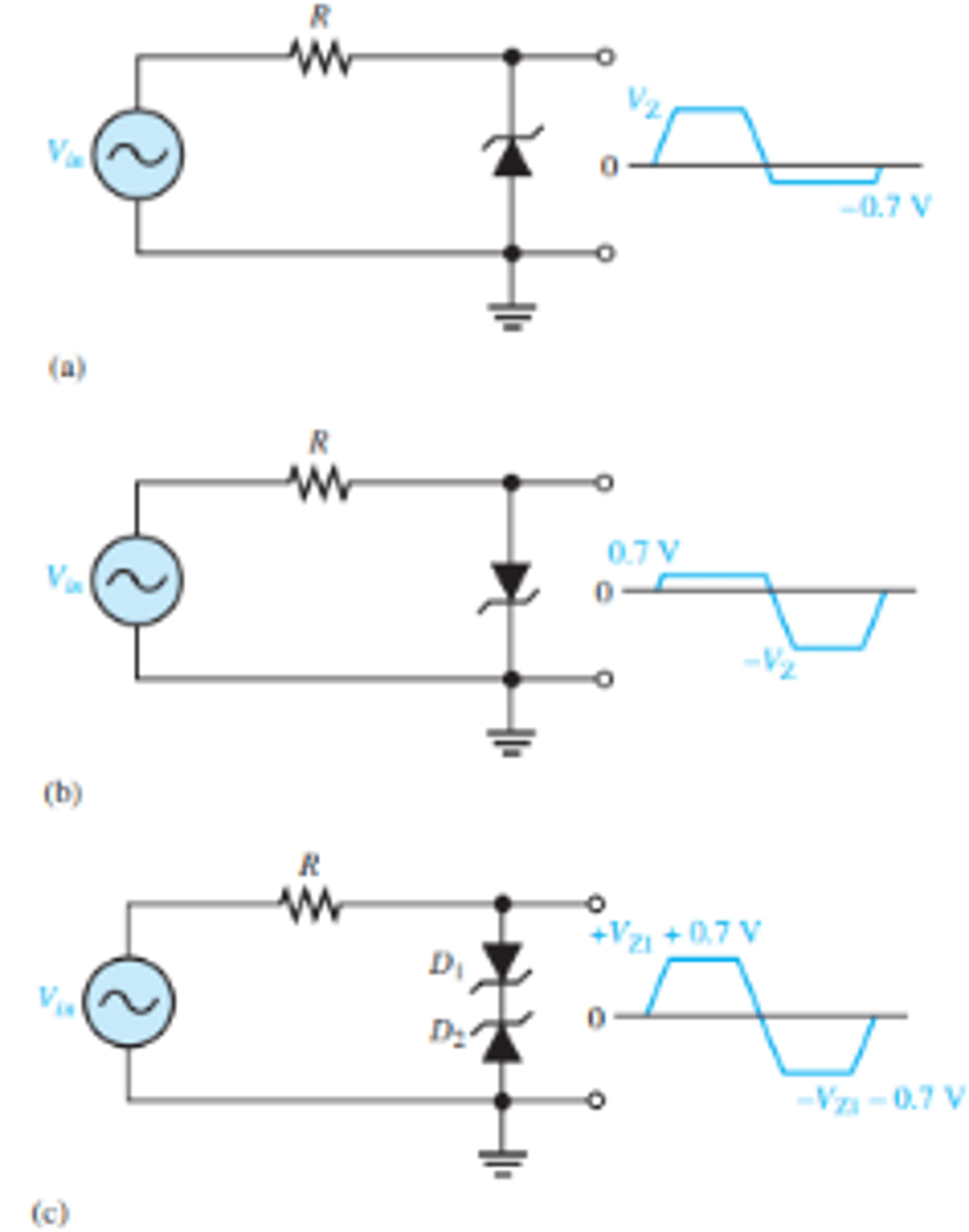
What are the 3 basic setups and their outputs for a zener limiter?
What is the forward bias for an LED show?
The forward voltage across an LED is considerably greater than for a silicon diode.
Typically, the maximum VF for LEDs is between 1.2 V and 3.2 V, depending on material.
An increase in IF corresponds proportionally to an increase in light output.
What is the circuit setup with an LED?