Inorganic Chemistry-revision
1/37
There's no tags or description
Looks like no tags are added yet.
Name | Mastery | Learn | Test | Matching | Spaced |
|---|
No study sessions yet.
38 Terms
1. In electrical terms, define:
a. Insulator,
b. Conductor,
c. Semi-conductor.
a. Insulator
Definition: A material that does not easily allow the flow of electric current.
Reason: It has a very high electrical resistance and no free electrons in its valence band.
Examples: Rubber, glass, plastic, ceramics.
b. Conductor
Definition: A material that allows electric current to flow easily.
Reason: It has a low electrical resistance and a large number of free electrons (delocalised electrons).
Examples: Copper, silver, aluminium, gold.
c. Semiconductor
Definition: A material with electrical conductivity between a conductor and an insulator.
Reason: It behaves as an insulator at low temperatures but can conduct when energy (e.g., heat or light) is added.
Properties:
Conductivity can be controlled by doping and temperature.
Used in transistors, diodes, and integrated circuits.
Examples: Silicon (Si), Germanium (Ge), Gallium Arsenide (GaAs).
2. What is the temperature dependence on the electrical conductivity of a:
a. Metal,
b. Semi-conductor.
a. Metal
In metals, electrical conductivity decreases as temperature increases. This happens because metals already have a large number of free electrons. When the temperature rises, the metal’s atomic lattice vibrates more intensely, causing more frequent collisions (or scattering) between the electrons and atoms. These collisions hinder the flow of electrons, which increases resistance and reduces conductivity.
b. Semiconductor
In semiconductors, electrical conductivity increases with temperature. At low temperatures, there are very few free charge carriers available, so the material behaves more like an insulator. As the temperature rises, more electrons gain enough energy to move from the valence band to the conduction band. This creates more free carriers (electrons and holes), allowing the material to conduct electricity more effectively.
3. In band theory define:
a. Valance band
b. Conduction band
c. Bad gap (forbidden band)
d. Fermi-Level
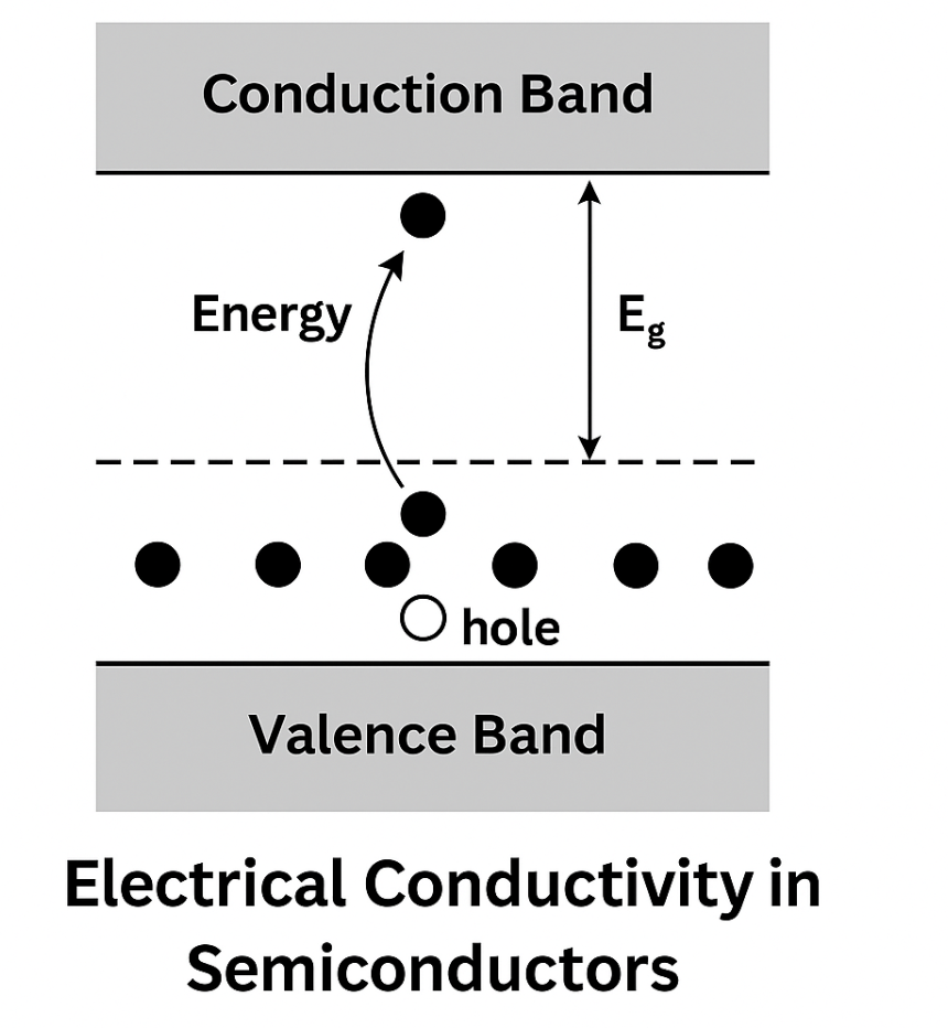
a. Valence Band
The valence band is the highest range of electron energies in a solid that is fully occupied by electrons at absolute zero temperature. It contains electrons that are bound to atoms and not free to move, meaning they do not contribute to electrical conduction unless excited to a higher energy level.
b. Conduction Band
The conduction band is the range of energies above the valence band where electrons are free to move within the material. Electrons in this band can conduct electricity, as they are no longer bound to atoms. For conduction to occur, electrons must gain enough energy to jump into this band from the valence band.
c. Band Gap (Forbidden Band)
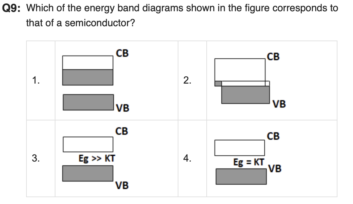
The band gap is the energy difference between the valence band and the conduction band. It represents a range of energies that electrons cannot occupy. The size of the band gap determines a material’s electrical properties:
Large gap → insulator,
Small gap → semiconductor,
No gap (overlapping bands) → conductor.
d. Fermi Level
The Fermi level is the highest occupied energy level at absolute zero. It represents the probability threshold where the chance of finding an electron is 50%. In metals, it lies within the conduction band; in semiconductors and insulators, it lies within the band gap. Its position influences how easily a material conducts electricity.
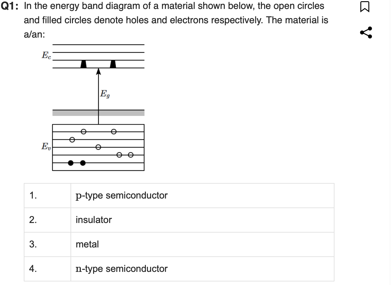
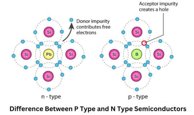
Correct Answer: 1. p-type semiconductor
Explanation:
In a p-type semiconductor, doping introduces acceptor levels, which create holes in the valence band.
Electrons are still present but are the minority carriers.
This matches the diagram, where the valence band has many holes and few electrons, and the conduction band is nearly empty.
Correct Answer: 4. Zero
Explanation:
In a good conductor (like metals), the conduction band and valence band either overlap or are partially filled, meaning there is no energy gap between them. Electrons can move freely with little or no energy input, which enables excellent electrical conductivity.
Zero band gap → free electrons are always available for conduction.
This contrasts with:
Insulators (very large/infinite band gap),
Semiconductors (small but non-zero band gap).
Correct Answer: 1. The resistivity of a semiconductor increases with an increase in temperature.
❌ Why It's Incorrect:
In a semiconductor, resistivity decreases as temperature increases. This is because higher temperatures provide energy for more electrons to move into the conduction band, increasing charge carriers and thus increasing conductivity (and decreasing resistivity).
✔ The other statements are correct:
2. Substances with an energy gap around 10 eV are indeed insulators.
3. In conductors, the valence and conduction bands overlap, allowing free movement of electrons.
4. The conductivity of a semiconductor increases with temperature, which is the correct behaviour.
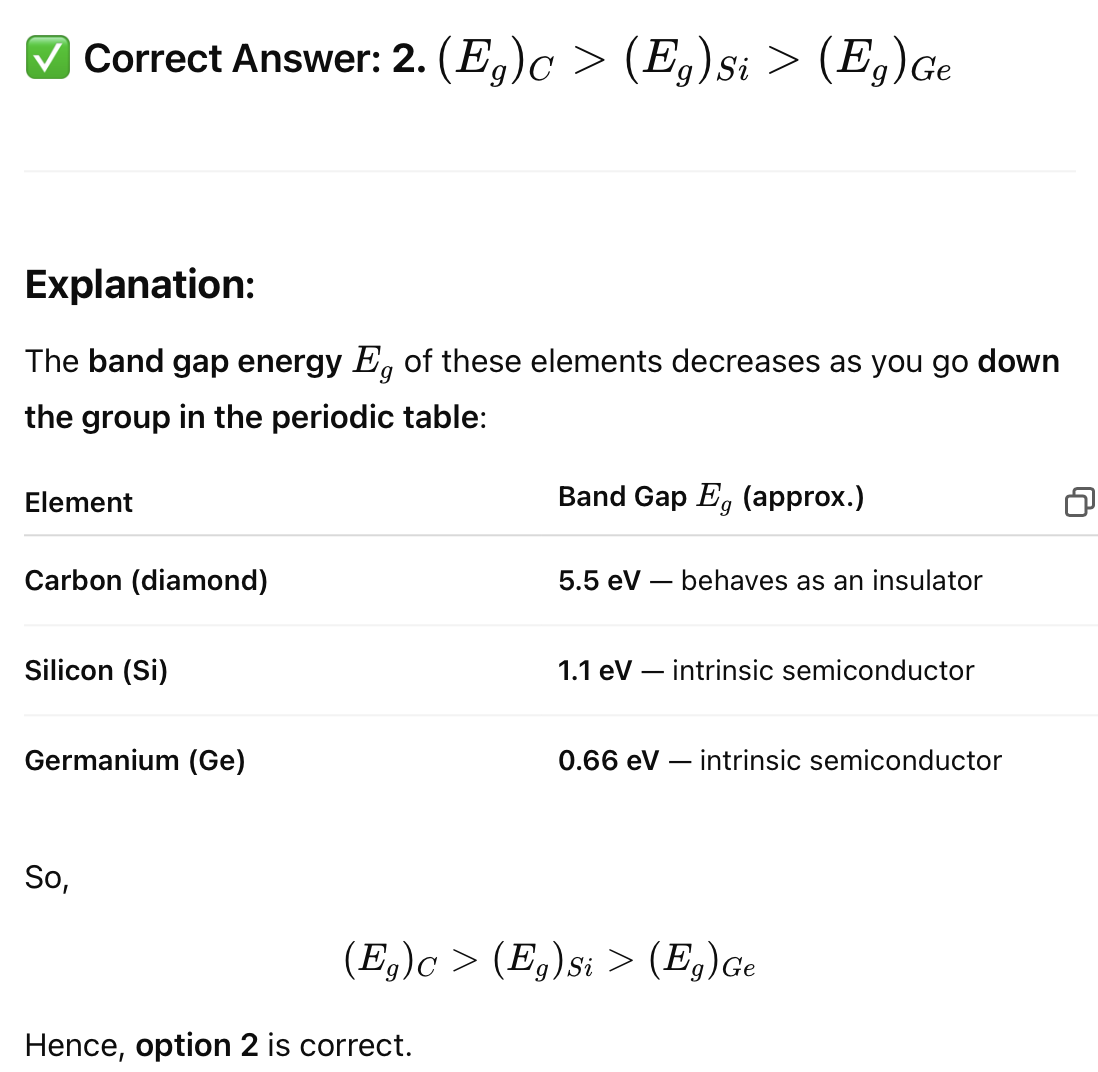
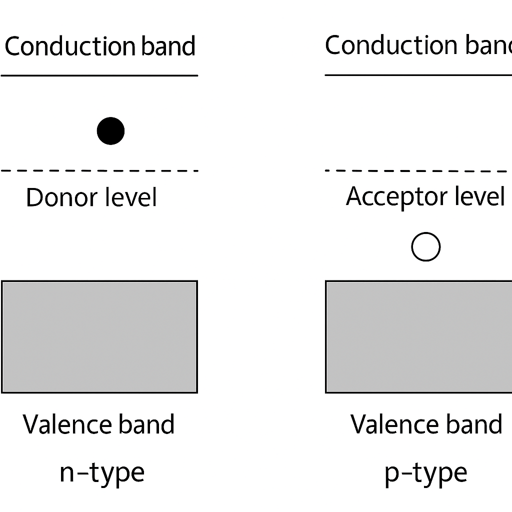
Correct Answer: 4. Sample X is undoped while samples Y and Z have been doped with a fifth group and a third group impurity respectively.
Explanation:
In semiconductor band diagrams, the position of the Fermi level (dashed line) indicates the doping type:
Sample X: Fermi level is in the middle of the band gap → this is characteristic of intrinsic (undoped) silicon.
Sample Y: Fermi level is closer to the conduction band → indicates n-type doping (using group V elements like phosphorus).
Sample Z: Fermi level is closer to the valence band → indicates p-type doping (using group III elements like boron).
Hence, sample X is undoped, Y is doped with a fifth group (n-type), and Z is doped with a third group (p-type).
Correct Answer: 4. The valence band is partially empty and the conduction band is partially filled.
Explanation:
At room temperature, a semiconductor absorbs enough thermal energy to:
Excite some electrons from the valence band to the conduction band,
Creating electron-hole pairs.
This means:
The valence band is partially empty (due to holes),
The conduction band is partially filled (due to excited electrons).
This behaviour allows semiconductors to conduct electricity, although not as well as metals.
So, Option 4 correctly describes the state of a semiconductor at room temperature.
Correct Answer: 4. 4000 Å
Correct answer = 4
Shows a small band gap where Eg=kT, which matches semiconductor behaviour at room temperature.
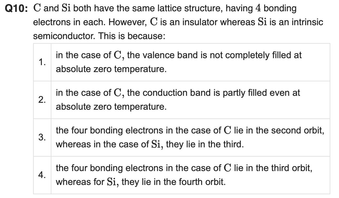
Correct Answer: 3.
"The four bonding electrons in the case of C lie in the second orbit, whereas in the case of Si, they lie in the third."
Using band theory diagram distinguish between a p- and n-type semiconductors.
What is the electrical conductivity mechanism in semi-conductor, i.e., how the electron jumps from the conduction band to the valence band.
In a semiconductor, electrical conductivity arises from the movement of charge carriers — electrons and holes — between the valence band and conduction band. Here's how it works:
1. At Absolute Zero (0 K)
The valence band is full, and the conduction band is empty.
No free charge carriers, so the material behaves like an insulator.
2. At Room Temperature or When Heated
Thermal energy excites some electrons in the valence band.
If the electron gains enough energy to overcome the band gap (EgEg), it jumps to the conduction band.
This creates:
A free electron in the conduction band (which can move and conduct electricity).
A hole in the valence band (a positive charge carrier that also contributes to conduction as neighbouring electrons fill it).
electron (valence band)→(energy≥Eg) →conduction band
3. External Energy Sources
Apart from heat, other sources can promote electrons:
Light (photons) in photoconductors or photodiodes.
Electric field in biased circuits.
Impurities (doping) reduce EgEg locally by adding donor or acceptor levels.
Summary:
Electrons jump from the valence band to the conduction band when they absorb enough energy to bridge the band gap, leaving behind holes. These electrons and holes move under an electric field, enabling semiconductivity.
Semi-conductor detectors are used in electron microscopy to detect backscattered electrons. How does the detector distinguish between backscattered and secondary
electrons.
In electron microscopy, semiconductor detectors (like Si(Li) or solid-state detectors) distinguish between backscattered electrons (BSEs) and secondary electrons (SEs) based on their energy and emission geometry. Here's how:
1. Energy Difference
Backscattered Electrons (BSEs):
High energy (typically 50–100% of the incident beam energy).
Result from elastic scattering of primary electrons with atomic nuclei.
Secondary Electrons (SEs):
Low energy (<50 eV).
Emerge from inelastic interactions with atomic electrons near the surface.
Semiconductor detectors can filter signals based on electron energy. By adjusting the bias voltage or using energy-sensitive electronics, they can discriminate SEs from BSEs.
2. Detector Position and Geometry
SE detectors (e.g. Everhart–Thornley detector) are placed near the sample to catch low-energy SEs that can’t travel far.
BSE detectors are typically positioned above the sample or coaxially with the beam, allowing them to capture higher-energy BSEs, which are emitted in a broader angular range.
3. Timing and Signal Amplification
BSEs generate stronger signals in the detector due to their high energy.
SEs produce weaker, delayed signals that are often amplified differently.
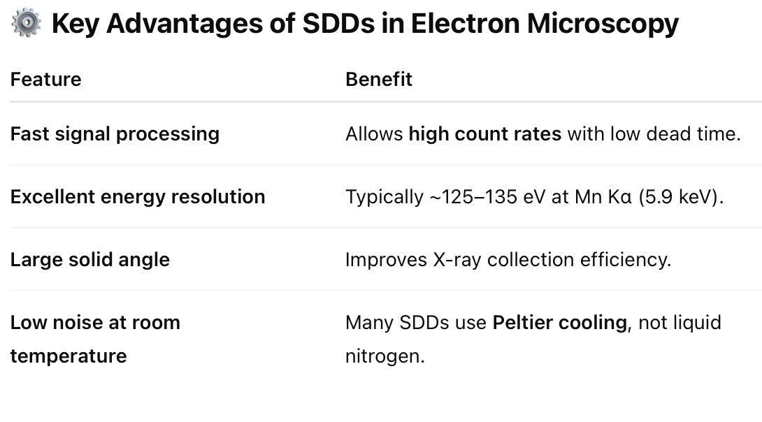
8. Describe how silicon drift detectors work for the detection of x-ray signals in electron microscopy.
Silicon Drift Detectors (SDDs) are advanced solid-state detectors used in Energy Dispersive X-ray Spectroscopy (EDS) systems attached to Scanning Electron Microscopes (SEMs) or Transmission Electron Microscopes (TEMs). They detect characteristic X-rays emitted when the electron beam excites atoms in the sample.
🔍Working Principle of SDDs
X-ray Photon Absorption
When an X-ray from the sample strikes the active silicon layer of the SDD, it ionises atoms in the silicon, creating electron-hole pairs.
The number of pairs is proportional to the energy of the incident X-ray photon.
Drift Ring Electrodes
A series of concentric biased ring electrodes create an electric field that guides the electrons toward a small central anode.
This drift field allows for fast and efficient collection of charge, even over a large detector area.
Charge Collection and Measurement
The collected electrons form a pulse.
The pulse height (amplitude) is directly related to the energy of the incoming X-ray.
This signal is amplified and digitised to generate an energy spectrum.
Summary:
Silicon Drift Detectors work by converting X-ray energy into an electrical signal via electron-hole pair generation in silicon. Their unique electrode structure enables fast, accurate, and high-throughput elemental analysis in electron microscopy.
Physical Chemistry
Distinguish between absorbance, fluorescence, phosphorescence and delayed fluorescence.
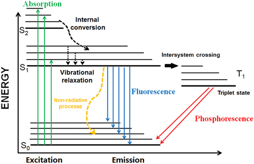
1. Absorbance
Definition: The process by which a molecule absorbs light energy, promoting an electron from a ground state (S₀) to an excited singlet state (S₁, S₂, etc.).
Time scale: Femtoseconds (10⁻¹⁵ s).
No emission occurs—energy is taken in, not released as light.
Used in: UV-Vis spectroscopy.
2. Fluorescence
Definition: Rapid emission of light as the electron returns from the first excited singlet state (S₁) to the ground state (S₀).
Time scale: Nanoseconds (10⁻⁹ to 10⁻⁸ s).
Energy loss: Some energy is lost via vibrational relaxation, so emitted light is lower in energy (longer wavelength) than absorbed light.
Spin state: Singlet → Singlet (allowed transition).
3. Phosphorescence
Definition: Delayed emission of light that occurs after the electron undergoes intersystem crossing to a triplet excited state (T₁) and then returns to the ground state (S₀).
Time scale: Microseconds to minutes (very slow).
Spin state: Triplet → Singlet (forbidden transition → slow).
Seen in: Glow-in-the-dark materials.
4. Delayed Fluorescence
Definition: Emission that resembles fluorescence but is delayed due to an intermediate step—commonly due to:
Triplet–triplet annihilation (two triplets collide to produce one S₁),
Or thermally activated delayed fluorescence (TADF).
Time scale: Microseconds to milliseconds.
Spin state: Ends with Singlet → Singlet, like fluorescence.
Looks like fluorescence but lasts longer.
Distinguish between spontaneous and stimulated emission.
Spontaneous Emission
Definition: The natural emission of a photon by an excited atom or molecule without external influence.
Mechanism: An electron in an excited state drops to a lower energy state and emits a photon randomly in direction and phase.
Photon properties:
Random direction
Random phase
Fixed energy (equal to the energy difference between states)
Occurs in: Fluorescence, phosphorescence, LEDs, stars.
Time scale: Typically nanoseconds in atoms/molecules.
Stimulated Emission
Definition: Emission that occurs when an incoming photon stimulates an excited electron to drop to a lower energy state, releasing a second photon.
Mechanism: The emitted photon has the same energy, phase, direction, and polarization as the incident photon — producing coherent light.
Photon properties:
Same wavelength, direction, and phase as the stimulating photon
Occurs in: Lasers (Light Amplification by Stimulated Emission of Radiation)
Key advantage: Enables amplification of light.
3. What is meant by population inversion?
Population Inversion – Definition
Population inversion is a condition in which more atoms or molecules are in an excited energy state than in a lower energy state, opposite to what is typically observed in thermal equilibrium.
Why It’s Important
Under normal conditions, most particles occupy the ground state.
For stimulated emission to dominate over absorption (which is essential for laser action), there must be more particles in the excited state than in the ground state.
This creates a net amplification of light rather than its absorption.
How It Is Achieved
Population inversion is achieved using external energy through a process called pumping, such as:
Optical pumping (using light)
Electrical pumping (current in semiconductors)
Chemical or gas discharge pumping
Often involves three-level or four-level laser systems, where energy levels are carefully arranged to facilitate efficient inversion.
Summary:
Population inversion is a non-equilibrium condition where excited states outnumber ground states, enabling stimulated emission and laser amplification.
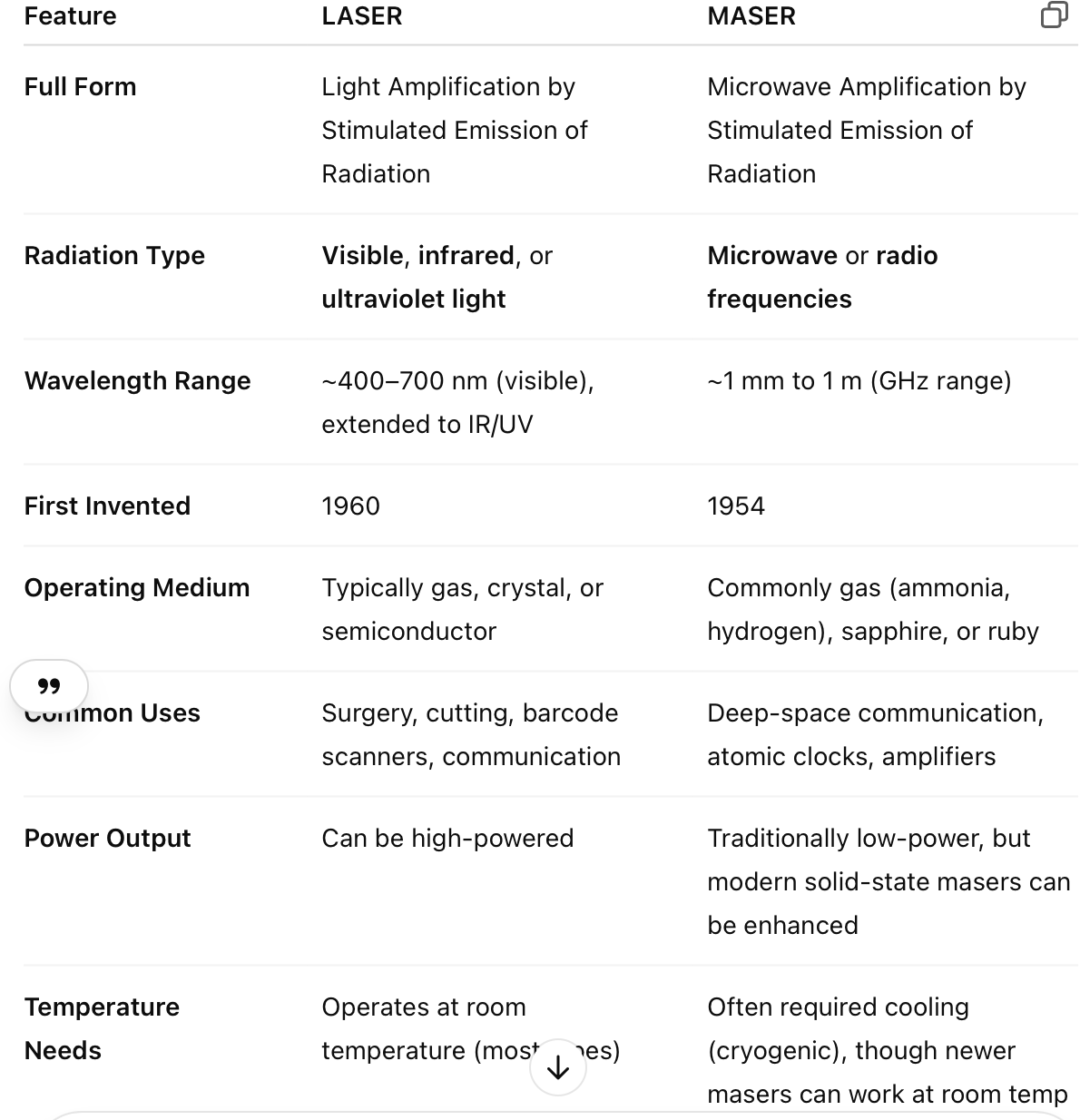
What does the acronym LASER and MASER mean.
LASER
Light Amplification by Stimulated Emission of Radiation
A laser produces a beam of coherent, monochromatic, and highly directional light.
Based on the principle of stimulated emission and population inversion.
Commonly used in: communication, medicine, cutting, measurement, and data storage.
MASER
Microwave Amplification by Stimulated Emission of Radiation
A maser operates on the same principle as a laser but emits microwave or radio-frequency radiation instead of visible light.
Was invented before the laser, originally for use in radar and atomic clocks.
Used in: deep-space communication, radio telescopes, and highly sensitive amplifiers.
What is the difference between a laser and maser?
While both lasers and masers operate on the same fundamental principle — stimulated emission — they differ in the type of electromagnetic radiation they amplify and some of their applications and technologies.
6. What are the conditions required for laser action?
Conditions Required for Laser Action
To produce laser light—that is, coherent, monochromatic, and directional electromagnetic radiation—three fundamental conditions must be met:
1. Population Inversion
Definition: More atoms or molecules must be in an excited energy state than in the ground state.
Why needed: To ensure stimulated emission dominates over absorption.
How achieved: Using an external pumping mechanism (optical, electrical, chemical, etc.).
2. Stimulated Emission
When an incoming photon causes an excited atom to drop to a lower energy state, emitting a second photon that is identical in energy, phase, direction, and polarization.
Core mechanism of laser amplification.
3. Optical Resonator (Cavity)
Typically consists of two mirrors facing each other around the gain medium.
One is fully reflective, the other is partially reflective (to allow output).
Function: Reflects photons back and forth through the gain medium, amplifying them via repeated stimulated emission.
Ensures coherence and directionality of the laser beam.
Optional but Important:
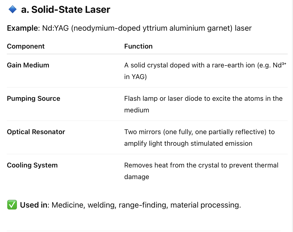
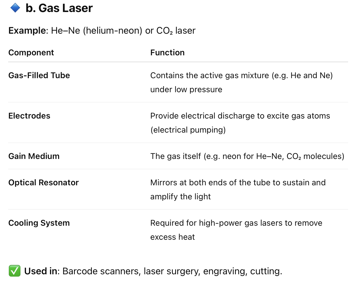
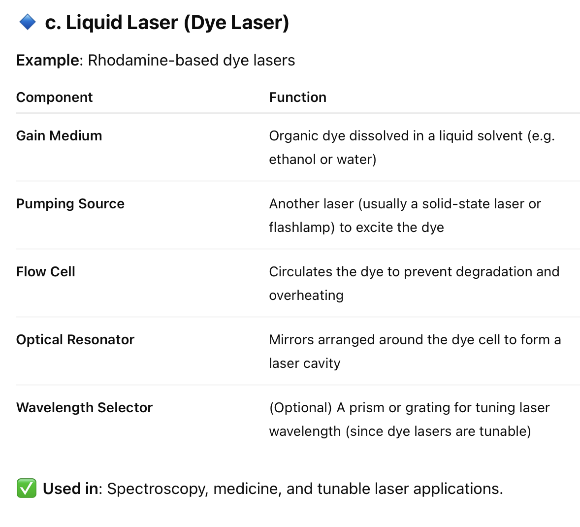
4. Gain Medium
The material in which population inversion and stimulated emission occur (e.g. ruby, Nd:YAG, He–Ne gas, semiconductor).
5. Pumping Source
Supplies external energy to excite atoms (e.g. flashlamp, electrical discharge, another laser).
7. In a laser, what is meant by a meta-stable state.?
A metastable state in a laser is an excited energy level where electrons can remain longer than usual before decaying. It is not the ground state, but it has a relatively long lifetime compared to other excited states—typically in the microsecond to millisecond range.
8. What are the main components required to:
a. Solid-state laser
b. Gas laser
c. Liquid laser
Engineering Physics Questions and Answers – Laser
This set of Engineering Physics Multiple Choice Questions & Answers (MCQs) focuses on “Laser”.
1. Which of the following is a unique property of laser?
a) Directional
b) Speed
c) Coherence
d) Wavelength
Answer: c
Explanation: Coherence is an important characteristic of laser beam because in laser beams, the wave trains of the same frequency are in phase/ Due to high coherence it results in extremely high power.
2. Which of the following is an example of optical pumping?
a) Ruby laser
b) Helium-Neon laser
c) Semiconductor laser
d) Dye laser
Answer: a
Explanation: The atoms of Ruby are excited with the help of photons emitted by an external optical source. The atoms absorb energy from photos and raises to excited state. Therefore Ruby laser is an example of optical pumping.
3. When laser light is focussed on a particular area for a long time, then that particular area alone will be heated.
a) True
b) False
Answer: a
Explanation: Laser beam has very high intensity, directional properties and coherence. When it is focussed on a particular area for a long time, then the area alone will be heated and the other area will remain as such. This is called thermal effect.
4. Calculate the wavelength of radiation emitted by an LED made up of a semiconducting material with band gap energy 2.8eV.
a) 2.8 Å
b) 4.3308 Å
c) 5548.4 Å
d) 4430.8 Å
Answer: d
Explanation: E = hc/ʎ
Therefore, ʎ = hc/E
ʎ = 4430.8 Å.
5. Calculate the number of photons, from green light of mercury (ʎ = 4961 Å), required to do one joule of work.
a) 4524.2×1018/m3
b) 2.4961×10¹⁸/m3
c) 2.4961/m3
d) 2.4961/m
Answer: b
Explanation: E = hc/ʎ
E = 4.006×10⁻¹⁹ Joules
Number of photons required = (1 Joule)/(4.006×10-19)
N = 2.4961×10¹⁸/m3.
6. Which of the following is ideal for the generation of laser pulse?
a) Ruby laser
b) Carbon dioxide laser
c) Helium neon laser
d) Nd-YAG laser
Answer: d
Explanation: Since Nd YAG laser has a higher thermal conductivity than other solid state lasers, it lends itself for the generation of laser pulses at a higher pulse repetition rate or a quasi continuous wave operation.
7. What is the need to achieve population inversion?
a) To excite most of the atoms
b) To bring most of the atoms to ground state
c) To achieve stable condition
d) To reduce the time of production of laser
Answer: a
Explanation: When population inversion is achieved, the majority of atoms are in the excited state. This causes amplification of the incident beam by stimulated emission. Thus the laser beam is produced.
8. Laser is called as a non-material knife.
a) False
b) True
Answer: b
Explanation: In laser surgery, without knife, bloodless operation, cutting tissues etc can be made, hence laser is called non-material knife.
9. DVD uses the laser.
a) True
b) False
Answer: a
Explanation: A DVD player contains a laser. By moving the lens longitudinally, different depths can be reached in the disc. In order to make room for a lot of information on every disc, the beam has to be focused on as small an area as possible. This cannot be done with any other light source.
10. Which of the following is used in atomic clocks?
a) Laser
b) Quartz
c) Maser
d) Helium
Answer: c
Explanation: Before laser maser was used. It stood for microwave amplification by stimulated emission of radiation. This was based on Albert Einstein’s principle of stimulated emission. It was used in the atomic clock.
11. Which of the following can be used in the vibrational analysis of structure?
a) Maser
b) Quarts
c) Electrical waves
d) Laser
Answer: d
Explanation: Laser can be used in the vibrational analysis of the structure. This is because when a structure under test begins to vibrate a distinctive pattern begins to emerge.