Higher physics: Unit 3 Electricity - p-n junctions
1/22
There's no tags or description
Looks like no tags are added yet.
Name | Mastery | Learn | Test | Matching | Spaced | Call with Kai |
|---|
No study sessions yet.
23 Terms
What are p-n junctions?
A fundamental building block of many other semiconductors electronic devices such as transistors, solar cells, light emitting diodes and integrated circuits.
Describe how p-n junctions are made?
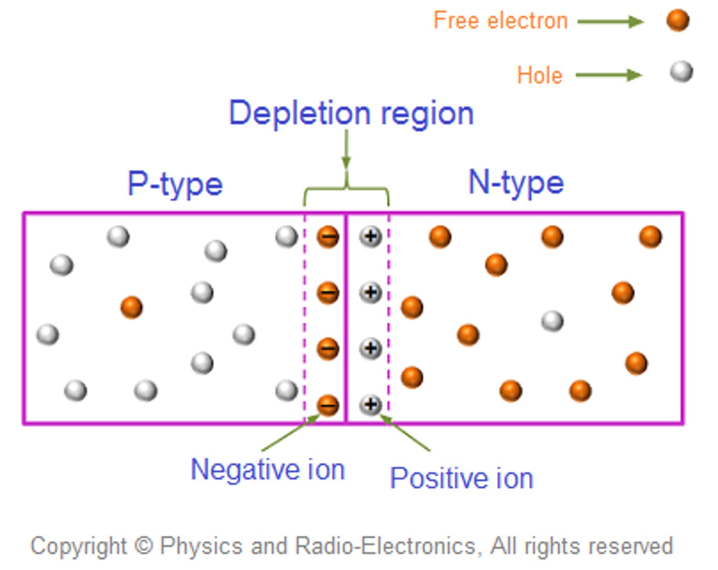
When a diode is first made there are free electrons in the n-type material and free holes in the p-type, although both sides are electrically neutral. The holes and electrons attract each other, leaving behind ions. Free electrons are more concentrated in the n-type and they diffuse across the junction and combine with some off the holes. The holes and electrons combine, having the creating a middle section with no excess charges called the depletion layer.
Why are p-n junctions insulators?
The holes and electrons combine at the junction, having the effect of creating a middle section with no excess charges (no charge carriers) called the depletion layer. This potential barrier stops further movement of charges, so the junction acts as an insulator

What forms the potential barrier in an unbiased p-n junction?
The electric field created as a result of the conduction band in the n-type material lowering and the valence band in the p-type material rising, which means the slope of the depletion layer increases.
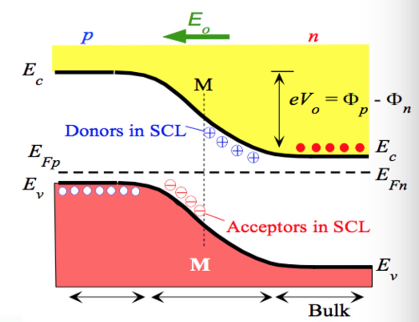
What forms the built-in-voltage/ potential barrier across the junction in an unbiased p-n junction?
The electric field created due to the charge separation on either side of the junction. As the conduction band in the n-type material lowers and the valence band in the p-type material rises, the gradients of the slope of the depletion layer increases.
For an unbiased p-n junction to conduct, what must first be overcome?
The electric field that acts as a potential barrier.
What is energy from an external source required for in an unbiased p-n junction?
To move the electrons 'uphill' from the n-type to p-type conduction band; and to move the holes 'downhill' from p-type to n-type valence band.

in forward bias, what is the charge on each end of the p-n junction?
The p-type is positively charged and the n-type is negatively charged.
Why is it easier for electrons to flow across the potential barrier in forward bias?
The p-type side is more positive, so that it is 'downhill' for electron motion across the junction and reduces the slope in the depletion layer.
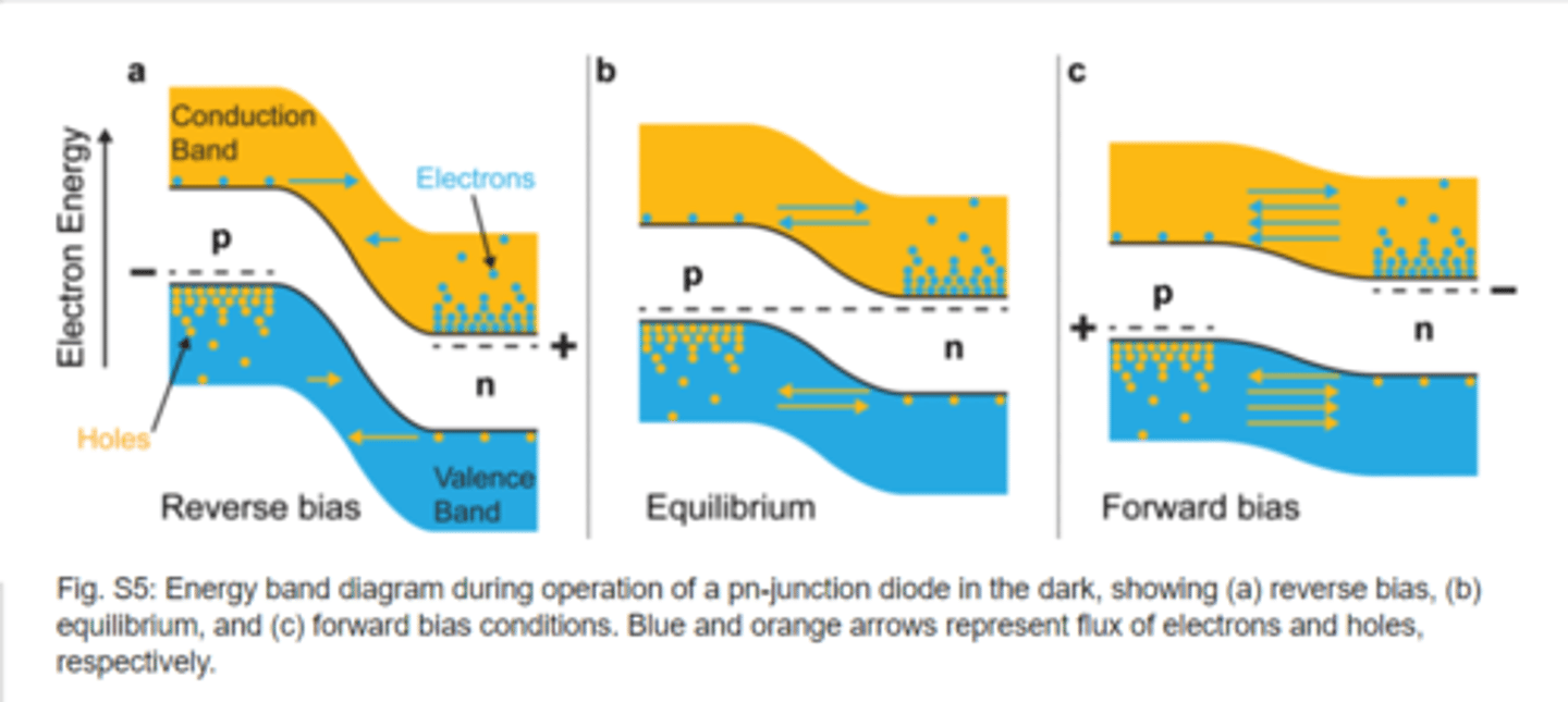
Describe how a hole can move right in a forward bias p-n junction?
An electron can move across the junction and fill a vacancy/ hole near the junction. It can then move from vacancy to vacancy leftward towards the positive terminal, so the hoe looks like it's moving right.
How can a diode in forward bias conduct?
The supply voltage increased beyond the magnitude of the electric field. The electrons in the n-type material which have been elevated to the conduction band and diffused across the junction find themselves at a higher energy than the holes in the p-type material. They readily combine with the holes, making a continuous forward current through the junction. This also has the effect of reducing the electric field of the depletion layer.
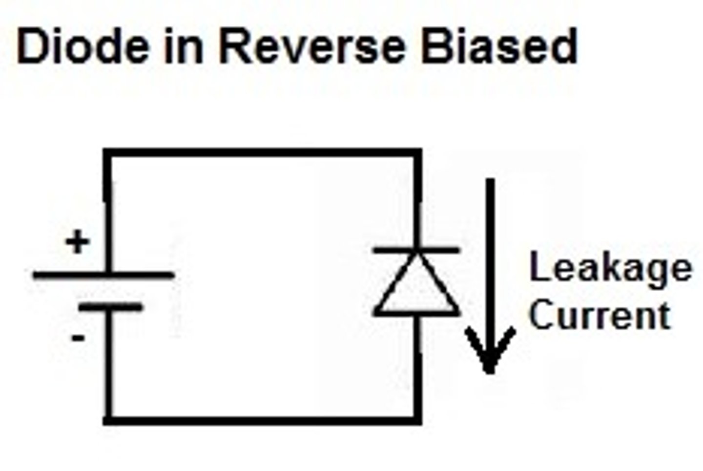
In reverse bias, what is the charge on the n-type and p-type ends?
P-type is negative, n-type is positive
In reverse bias, why does the depletion layer increase in width?
The free electrons in the n-type material will be attracted by the positive terminal of the supply battery and the electrons from the battery will enter the p-type end of the diode and combines with some of the holes. This has the effect of removing some of the charge carriers from the diode and increases the width of the depletion layer.

Why does a diode in reverse bias not conduct?
Charge carriers are removed from the diode, the width of the depletion layer has increased so the electric field of the junction becomes very large so there is no current in the circuit.
Describe the circuit that contains a reverse bias
N-type end facing the positive side of the power supply
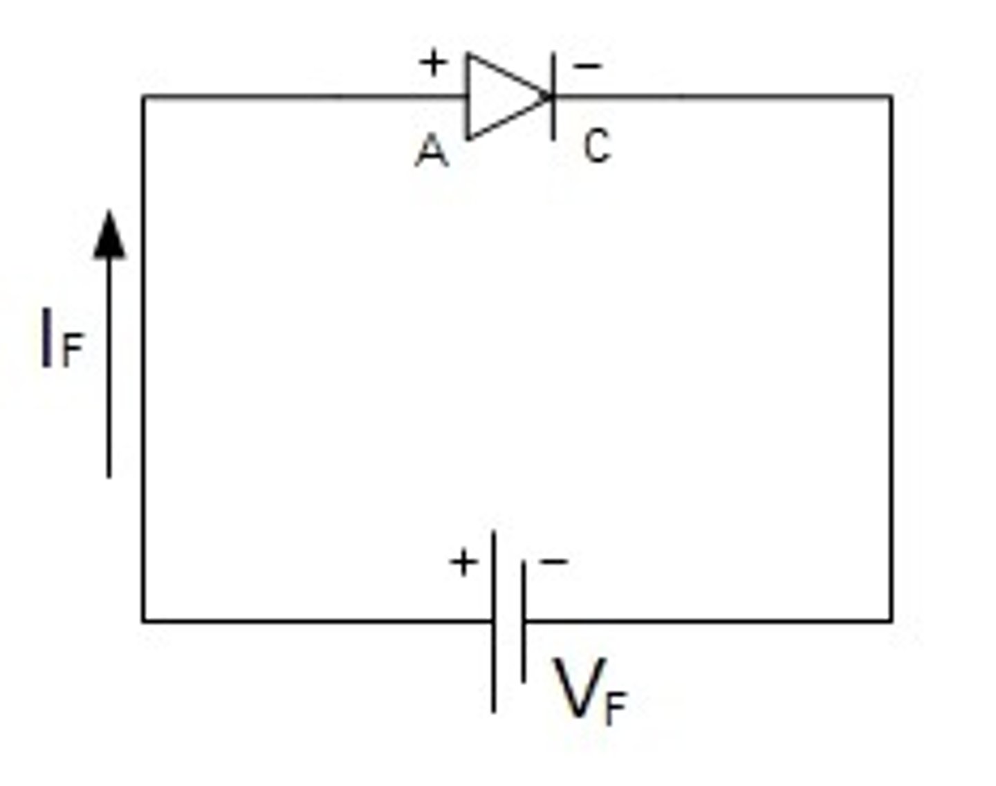
Describe the circuit that contains a forward bias
N-type end facing the negative side of the power supply
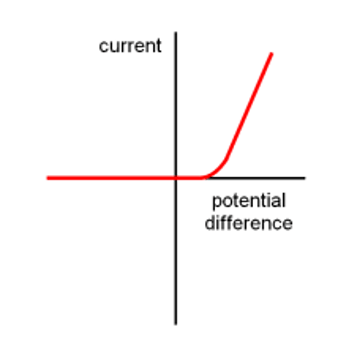
Describe the current - voltage graph of p-n junctions and what does it show?
No current in reverse bias;
A minimum forward bias voltage is required before the current can flow;
This minimum forward bias voltage is required to overcome the junction voltage which is across the depletion layer;
As the forward bias voltage increases above the junction voltage the current through the p-n junction diode increases;
The current is not proportional to the voltage across the diode.
What bias are LEDs in?
Forward
How do LEDs work?
The applied potential difference drives conduction band electrons into the depletion zone. They combine with holes arriving in the valence band from the p-type material. The energy lost by the electrons as they fall is emitted as photons.
What is the relationship between the energy of the recombination between the electron and hole and the energy of the emitted photon in an LED?
The same
What is colour of the emitted photon determined by?
The semiconductor material used
What is a photodiode?
A p-n junction in reverse bias used to turn light energy into electrical energy.
What is the photovoltaic effect?
When light on a p-n junction creates a voltage across the junction. Photons of light are absorbed at the junction. This produces a pair of charge carriers. An electron that goes into the conduction band of the n-type and a hole that goes into the valence band of the p-type, generating a voltage.