Semiconductors
1/83
There's no tags or description
Looks like no tags are added yet.
Name | Mastery | Learn | Test | Matching | Spaced |
|---|
No study sessions yet.
84 Terms
What determines how well a solid conducts electricity?
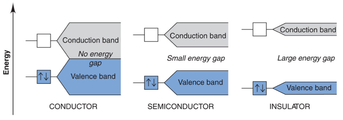
The distance between the valence + conduction bands — smaller gaps allow easier electron movement + higher conductivity.
How do conductors, semiconductors + insulators differ in terms of band gap?
conductors: overlapping VB + CB
easy for electrons to move between bands
semiconductors: small gaps
still possible for electron to move between bands (depends on conditions)
insulators: large gaps
very hard for electrons to move across bands
What are some properties of Si?
diamond cubic structure with a space group of Fd-3m, each Si atom bonded to 4 others at 109.47°
band gap: 1.1 ev ➡ small enough to make it semiconductor
What is an intrinsic semiconductor?
pure material where electrons + holes are generated only by thermal excitation across the bandgap
holes: (+) charged vacancies that can move + carry current
both electrons + holes behave like charge carriers with their own mass, charge + mobility
What is the effect of temperature on intrinsic semiconductors?
Higher temperature increases electron excitation across the bandgap from VB to CB, increasing conductivity.
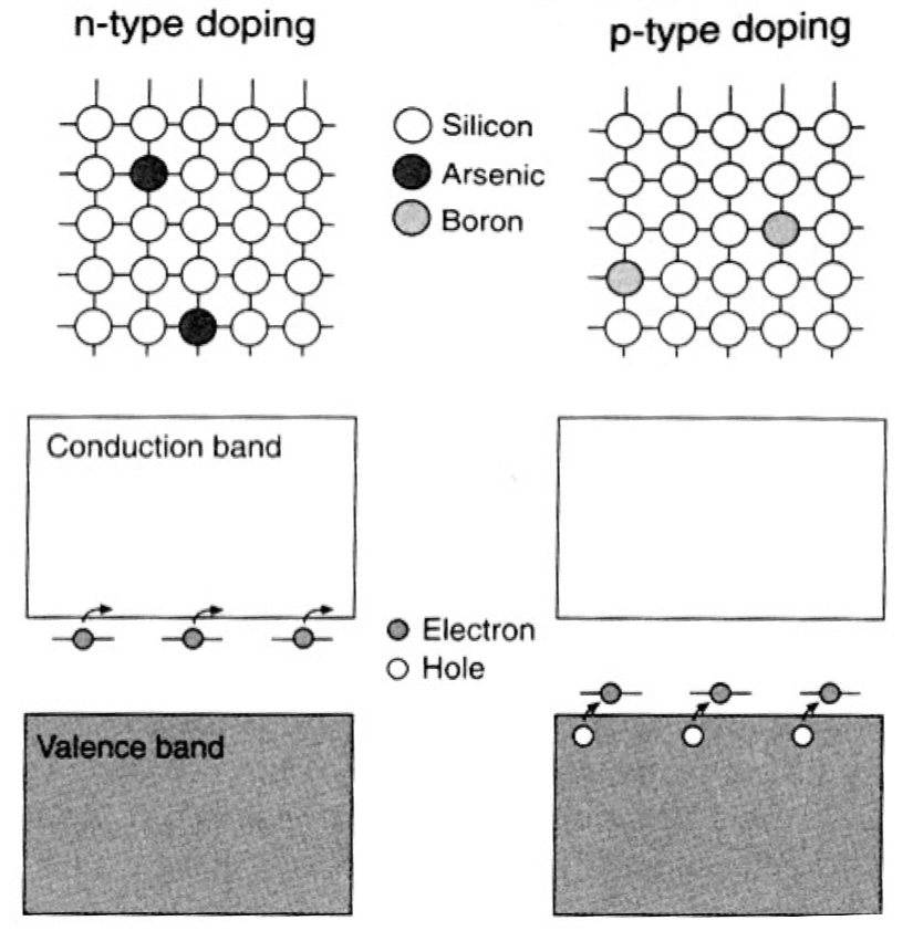
What’s the difference between n-type semiconductors VS p-type semiconductors
n-type:
doping Si with Group V elements (P, Ar) which have one more valence electron than Si
this extra electron occupies an energy level just below the CB, making it easy to excite into CB where it moves freely, providing conduction through electrons
p-type:
doping Si with Group III elements (B, Al) which have one fewer valence electron than Si
this creates an energy level just above the VB, allowing electrons from the VB to fill it + leaving behind mobile holes
conduction occurs through the movement of these holes in the valence band
Why are n-type + p-type semiconductors still overall neutral?
Number of protons equals the number of electrons, even though one type of carrier dominates conduction.
What is the Fermi energy?
represents the highest occupied electron energy level at absolute zero (0 k)
in doped semiconductors, the Fermi level shifts toward CB for n-type + toward VB for p-type, reflecting the dominant charge carrier type

What is the basic function of a transistor + how is it built using semiconductors?
transistor works as an electronic switch/gate that controls current
built from semiconductor materials (typically Si) that are doped into n-type + p-type regions to enable control over charge carriers
What does it mean when electrons move, the holes (H⁺) now appear in different positions?
when an electron leaves its spot in the VB, it creates an empty position called a hole
as nearby electrons move to fill that hole, they leave new empty spots behind
makes it seem like the hole itself is moving in the opposite direction of the electrons
even though only electrons physically move, the shifting of these empty spots behaves like the motion of (+) charge carriers, which is how conduction occurs in p-type semiconductors
What is the fermi level, and how do doping + structure affect the conductivity of semiconductors?
fermi level: energy level at which ½ the available electronic states are filled at a given temperature
at thermal equilibrium, ½ of available electron sates below fermi level are filled + ½ of those above it are empty
doping introduces new energy states within the band gap:
n-type: adds states just below the conduction band
p-type: adds states just above the valence band
changing the doping level changes the number of charge carriers + thus modulates conductivity
What is the structure of silicon’s main allotrope + how does orbital overlap affect its band gap?
Si’s main allotrope has a diamondoid lattice, where each atom is tetrahedrally bonded to 4 others
band gap depends on orbital overlap:
greater overlap decreases HOMO–LUMO (band) gap
smaller overlap increases HOMO-LUMO (band) gap
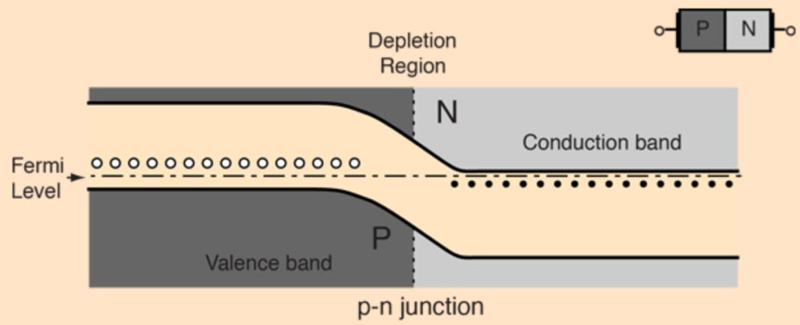
What happens when p-type + n-type semiconductors are brought into contact to form a PN junction?
electrons from n-type region diffuse into the p-type + holes from the p-type diffuse into the n-type
creates a depletion region depleted of charge carriers
this forms an electric field across the junction, resulting in a voltage drop (built-in potential) that opposes further diffusion movement + stabilizes the junction until external voltage is applied
What happens in a PN junction at equilibrium regarding diffusion, drift + energy levels?
at equilibrium: diffusion of electrons + holes is balanced by drift (pushing electrons back to n-type side + holes back to p-type side) caused by the electric field in the depletion region, so there’s no net current
the fermi levels of the p-type + n-type regions align
depletion region forms a natural energy barrier:
electrons must gain energy to move up in energy
holes must gain energy to move down, preventing further carrier flow
What happens to a PN junction under reverse bias + how does it affect electron conduction?
p-side is connected to (-) terminal of power source + n-side to (+) terminal
depletion region + the energy barrier increases, making it “uphill” for electrons to cross the junction, so very little current flows
junction acts like a switch in the off position, with electron flow energetically opposed by the larger barrier
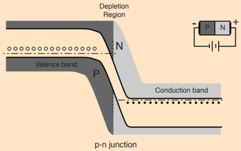
What happens to a PN junction under forward bias + how does electron conduction occur?
p-side is connected to (+) terminal of power source + n-side to (-) terminal,
this reduces depletion region + lowers the energy barrier
electrons from n-type side can move downhill across the junction, filling holes in the p-type region, effectively allowing current to flow
junction acts like diode switch in the on position, with electron conduction from right to left + holes appearing to move in the opposite direction
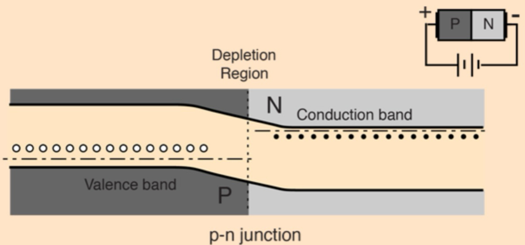
What is a PN junction diode + how does it function?
semiconductor device that allows current to flow in only one direction
when diode is forward biased (p-side (+) + n-side (-)): electrons can flow from n-type to p-type, allowing current to pass
when diode is reversed biased (p-side (-) + n-side (+)): depletion region barrier increases + little current flows
used for rectification in DC power supplies + in applications like AM radio
What are the types + structure of a MOSFET + how does it function?
N-channel (Nmoss) FETS use electrons as charge carriers:
p-channel (PMOS) FETS use holes
mosfet has:
source terminal: where current enters device
drain terminal: where current exits device
gate terminal: controls flow of charge carriers between source + drain
gate oxide: insulating layer between gate + semiconductor channel, allowing gate voltage to control the channel without direct flow
operation principle:
applying voltage to the gate controls the conductivity of the channel between source + drain, allowing the device to function as a switch or amplifier
NMOS uses electrons in the channel; PMOS uses holes
What is Moore’s Law?
Observation that the number of transistors on an integrated circuit doubles around ever 2 years, leading to increased performance + decreased relative cost of electronics over time.
What is photolithography?
enables creation of intricate patterns on Si wafers to form integrated circuits
types of photoresist:
positive: the areas exposed to light become more soluble in the developer, allowing them to be washed away, leaving the unexposed areas intact (light is removed)
negative: the areas exposed to light become less soluble, hardening the photoresist + leaving the exposed regions on the wafer (light isn’t removed)
What is the Miracle Month?
Period from November 17-December 23 1947 where scientists created first functioning transistor by submerging a Si-based device in water (led to significant amplification).
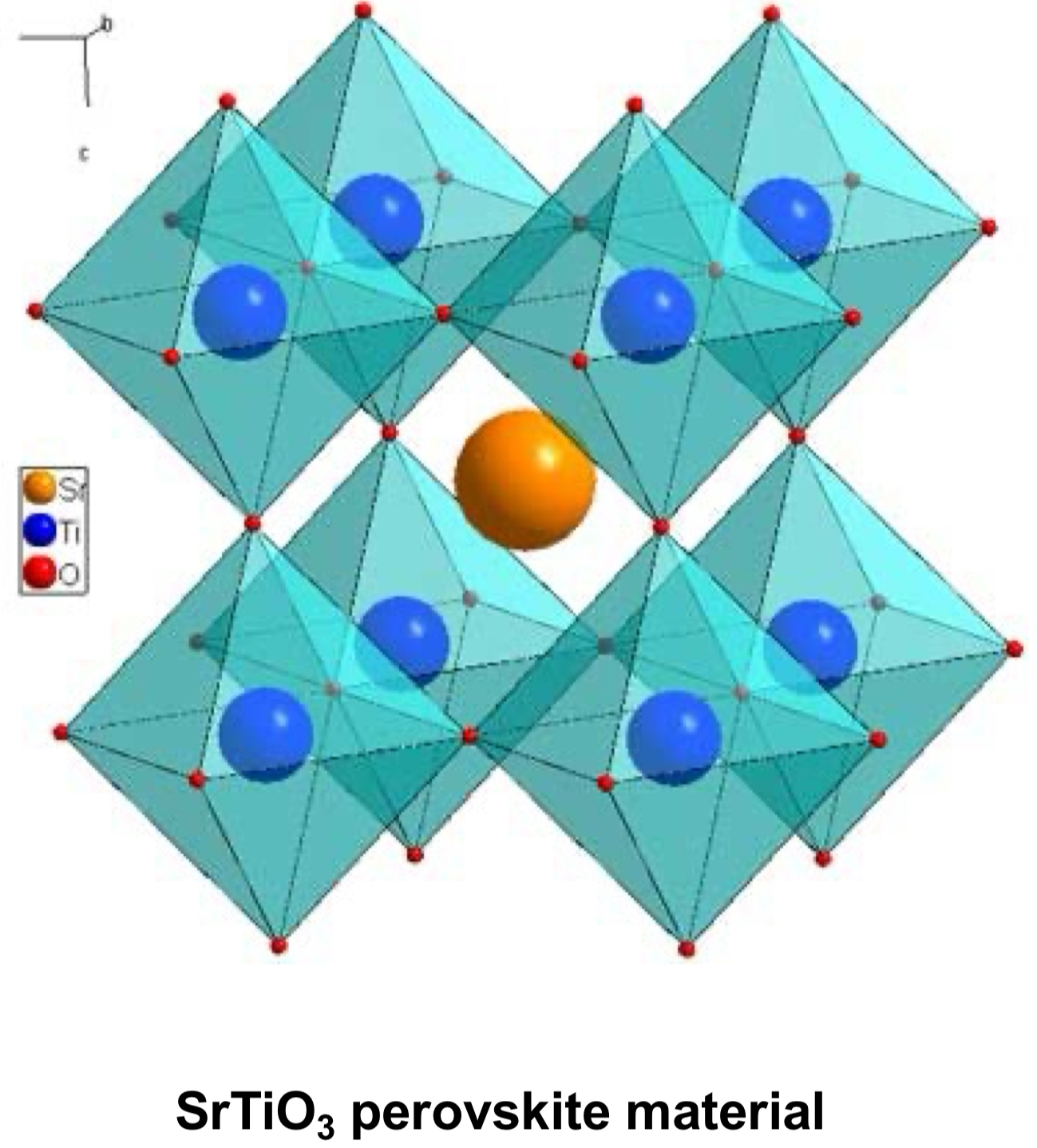
What is the general chemical formula for perovskites + what do the letters represent?
perovskites have the general formula ABX₃
A: large cation that sits in large spaces between structures (orange)
B: smaller cation that sits inside octahedra (blue)
X: anion that forms corners of those octahedra (red)
What does the Goldschmidt Tolerance Factor describe in perovskites?
Predicts whether ions of certain sizes can form a stable Perovskite structure by comparing the relative sizes of the A, B + X ions.
What is the charge-balanced formula for a typical perovskite + how can it vary with anions?
typical charge-balanced formula: A²⁺B⁴⁺(X²⁻)₃
if the anion is monovalent (x⁻), formula becomes A⁺B²⁺(X⁻)₃ to maintain charge neutrality
What is MAPI (methylammonium lead triiodide) + what makes its structure flexible?
MAPI: hybrid perovskite with formula ABX₃
flexible since its optical + electrical properties can be tuned
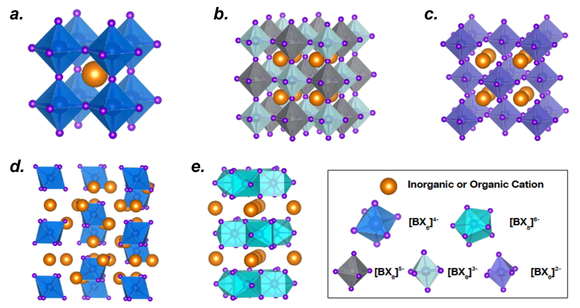
related types like vacancy-ordered, double + layered perovskites have similar but slightly different structures
What are the main types of crystal structures found in perovskite + perovskite-inspired materials?
3D perovskite: fully connected network of octahedra
double perovskite: alternating B-site cations (A₂BB′X₆)
vacancy-ordered: missing some B-sites, breaking connectivity
Ruddlesden-Popper (2D): layered perovskite sheets separated by organic cations
0D perovskite: isolated octahedra with strong light emission but low conductivity
How do Photovoltaic solar panels generate electricity + what are they made of?
contains many solar cells that convert sunlight into electricity through PN junctions
most panels use polycrystalline silicon
process is like an LED in reverse: instead of using electricity to make light, solar cells use light to make electricity
How do dye-sensitized solar cells (DSSCs) generate electricity + what materials are involved?
process:
beneath it is a high SA material (ex. TiO₂), which is a good conductor for electrons + provides lots of space for reactions to occur
attached to the TiO₂ is a light-absorbing dye or perovskite, which captures sunlight + releases electrons
these electrons flow through the circuit, while a liquid electrolyte moves (+) charges in the opposite direction to balance the charge
finally, a reflective back electrode sends electrons back into the system, completing the circuit + allowing continuous power generation
unlike silicon slabs, these cells rely on multiple materials working together
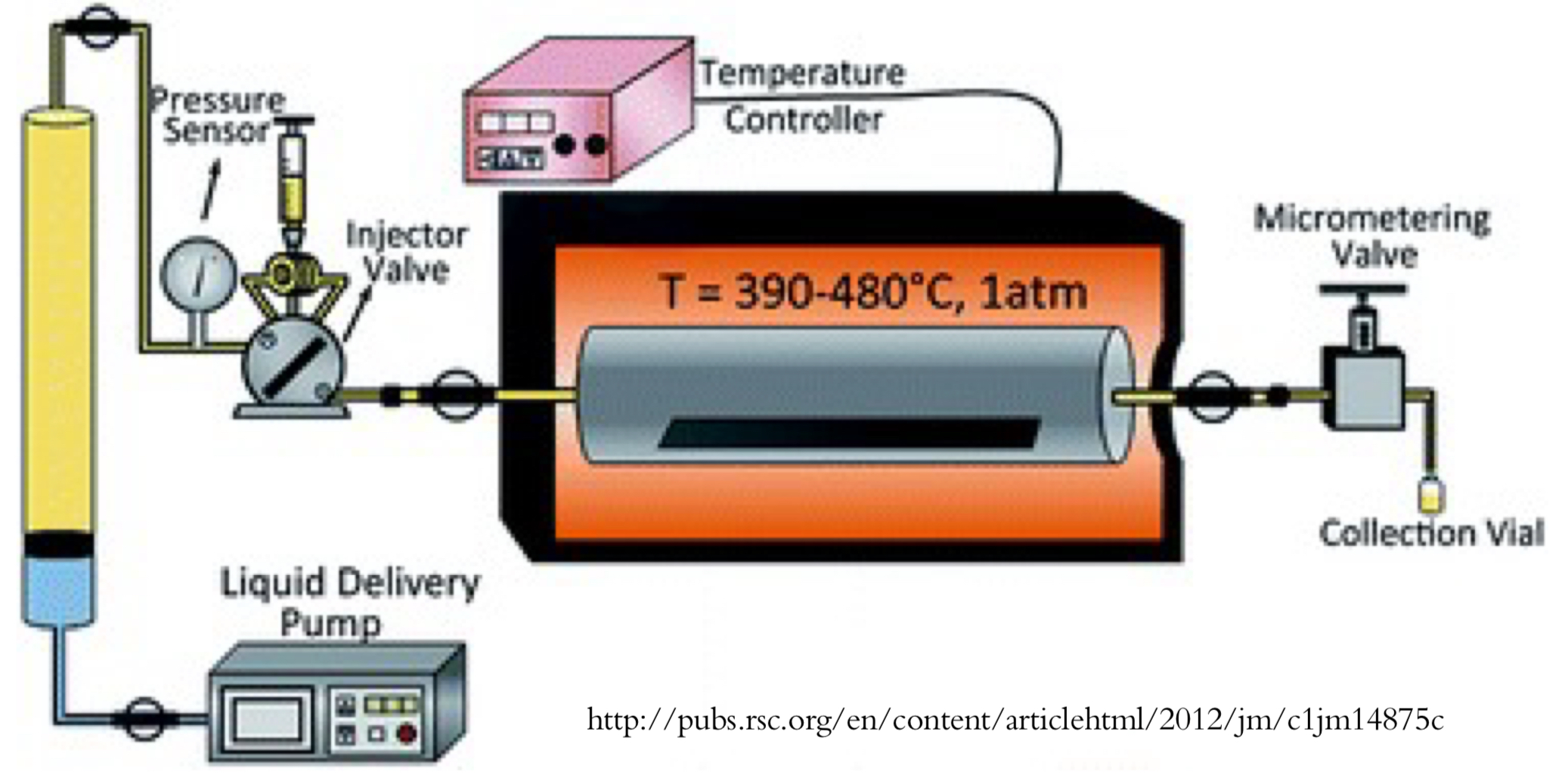
What is the purpose of controlling the molar ratio 1 : x : (1 − x) in CsBr, SnBr₂, + PbBr₂ during the synthesis of CsSnₓPb₁₋ₓBr₃?
It determines the relative amounts of Sn²⁺ + Pb²⁺ on the B-site of the Perovskite lattice, tuning the composition, bandgap, + optoelectronic properties.
Why are concentrated HBr + H₃PO₂ added during the solvent synthesis of CsSnₓPb₁₋ₓBr₃?
HBr dissolves the metal halides + supplies Br⁻ ions, while H₃PO₂ acts as a reducing agent to prevent oxidation of Sn²⁺ to Sn⁴⁺.
Why is nitrogen gas flowed continuously through the reaction vial in metal halide perovskite synthesis?
To maintain an inert, oxygen-free environment that protects Sn²⁺ from oxidation + ensures pure perovskite formation.
What happens during the 120 °C heating + 20 minute stirring step in metal halide perovskite synthesis?
The metal halide precursors dissolve + react in the acidic medium, forming perovskite nuclei that grow into fine CsSnₓPb₁₋ₓBr₃ crystals.
What are the key post-reaction steps to isolate the CsSnₓPb₁₋ₓBr₃ product?
cool the mixture
filter under reduced pressure
wash the solid with isopropyl alcohol to remove acid
dry to obtain the purified crystalline powder
How does increasing Sn content in CsSnₓPb₁₋ₓBr₃ affect its electronic properties?
narrows the bandgap, shifting optical absorption toward longer wavelengths (red shift) + improving carrier mobility
this allows for systematic control of the electronic properties for optoelectronic applications (solar cells, LEDs, photodetectors)
Why are the powders pressed into pellets and loaded into evacuated fused-silica tubes in high-T synthesis of CsSnₓPb₁₋ₓBr₃?
pellets improve contact between reactants for efficient solid-state diffusion
fused-silica tubes withstand high T
tubes are evacuated to 10⁻³ mbar + sealed to prevent oxidation of Sn²⁺ + contamination
Why is heating + cooling conditions important in high-T synthesis of CsSnₓPb₁₋ₓBr₃?
slow heating allows controlled reaction + uniform crystallization
slow cooling prevents thermal stress + undesired phase formation
What are the key principles behind high-temperature solid-state perovskite synthesis?
reactions are driven by solid-state diffusion
vacuum prevents Sn²⁺ oxidation
pelletizing ensures uniform reaction
slow heating + cooling control crystallization
quenching captures metastable phases
What happens during the ball-milling step of mechanochemical synthesis of CsSnₓPb₁₋ₓBr₃ + why is it important?
mixture is milled at 750 rpm for 30 minutes
milling process is repeated 3x to ensure all material reacts completely ➡ uniform, high-quality CsSn₀.₅Pb₀.₅Br₃ perovskite
mechanical energy breaks + reforms bonds, allowing the perovskite structure to form without solvent
What are the advantages of mechanochemical synthesis for perovskites?
solvent-free, reduces waste + uses mechanical energy to drive solid-state reactions
an inert nitrogen environment prevents Sn²⁺ oxidation
careful choice of milling speed + ball size ensures proper energy input without degradation
Why is mesitylene used as the solvent instead of ODE in nanoparticle perovskite synthesis?
Cs- + Pb-2-ethylhexanoate complexes are insufficiently soluble in ODE
mesitylene dissolves the complexes well, has a lower BP + can be dried and stored water-free in a glovebox
What are the key principles + precautions of nanoparticle perovskite synthesis?
maintains water-free conditions to prevent hydrolysis
uses zwitterionic ligands for colloidal stabilization
chooses mesitylene as a suitable solvent
triggers nucleation via TOP-halide injection to form CsPbX nanocrystals stabilized by zwitterionic ligands
What durability challenges do perovskite solar panels face compared to silicon panels?
Unclear if they can survive rain, wind, intense sunlight + freezing T for decades like silicon panels, which are expected to last ~25 years.
Why is the toxicity of perovskite solar cells a concern?
Most perovskite devices contain lead, which is toxic + raises concerns about handling, disposal, and environmental impact.
How do perovskite solar panels compare to conventional silicon panels in terms of market competition?
Silicon panels are already cheap + efficient, so new materials like perovskites must outperform them significantly to impact energy production + climate goals.
What is Sarah Kurtz’s perspective on perovskite solar cells?
She advises caution, saying they could help, but we shouldn’t rely on them alone to solve the world’s energy problems.
Why is matching the bandgap of a perovskite material to the solar spectrum important?
To achieve the highest solar cell efficiency by absorbing the right range of sunlight photons.
How can the absorption properties of perovskites be modulated most significantly?
By changing the halide ratio (Cl, Br, I) in the perovskite structure.
How can fine adjustments of perovskite bandgap + structure be achieved?
By changing the ratio of A-site cations (Cs⁺, MA⁺, FA⁺) + B-site cations (Pb²⁺, Sn²⁺, Ge²⁺).
What are the chemical formulas for the common A-site cations in perovskites?
MA (methylammonium): CH₃NH₃⁺
FA (formamidinium): CH(NH₂)₂⁺
Cs (cesium): Cs⁺
What are defects + why are defects considered bad in silicon devices?
defects: irregularity in the crystal lattice
ex. missing atom, misplaced ion
bad because they disrupt electron flow, which is critical for ultra-pure transistors + photovoltaic panels
How do Pb-halide perovskites handle defects compared to silicon?
they tolerate defects well + minor defects don’t significantly reduce device performance
silicon requires near-perfect crystals, whereas perovskites can function efficiently even with imperfections
What are the 3 main reasons why lead-halide perovskite nanocrystals are defect-tolerant?
crystal structure favours formation of vacancies but suppresses other defects
electronic structure places defect states as shallow traps or inside conduction/valence bands
dynamic lattice effects (ex. polaron formation) prevent carrier trapping
Which type of defect is most likely to occur in LHPs + why?
Vacancies, because they have the lowest formation energy among point defects.
What is a polaron + how does it help defect tolerance in perovskites?
polaron: charge carrier (electron or hole) surrounded by local lattice deformation
prevents the carrier from being trapped by defects, maintaining good optical + electronic performance
Why do defects in LHPs not strongly influence radiative recombination?
Because defect states in LHPs are shallow or lie inside conduction/valence bands, so they don’t act as deep traps that capture carriers.
How does the electronic structure of LHPs differ from conventional semiconductors regarding defects?
in LHPs: bandgap is between 2 antibonding orbitals, so defects form shallow traps or states inside the bands
in conventional semiconductors: defects create mid-gap states that strongly affect optical/electronic properties
Why is the NREL efficiency chart important for perovskite research?
serves as a benchmark to compare perovskite efficiency progress against mature technologies
helps identify how close perovskites are to commercial viability + tracks historical trends in efficiency
How does a light-emitting diode (LED) produce light?
in a PN junction made of a direct bandgap semiconductor, electrons + holes recombine, releasing energy as photons
the photon energy equals the semiconductor’s bandgap (Eg), determining the colour of the emitted light
Why do different semiconductor materials in LEDs emit different colours of light?
colour depends on the bandgap energy (Eg) of the material
ex. GaInN/GaN blue LEDs (470 nm); larger bandgap
ex. GaInN/GaN green LEDs (525 nm): moderate bandgap
ex. AlGaInP/GaAs red LEDs (625 nm): smallest bandgap
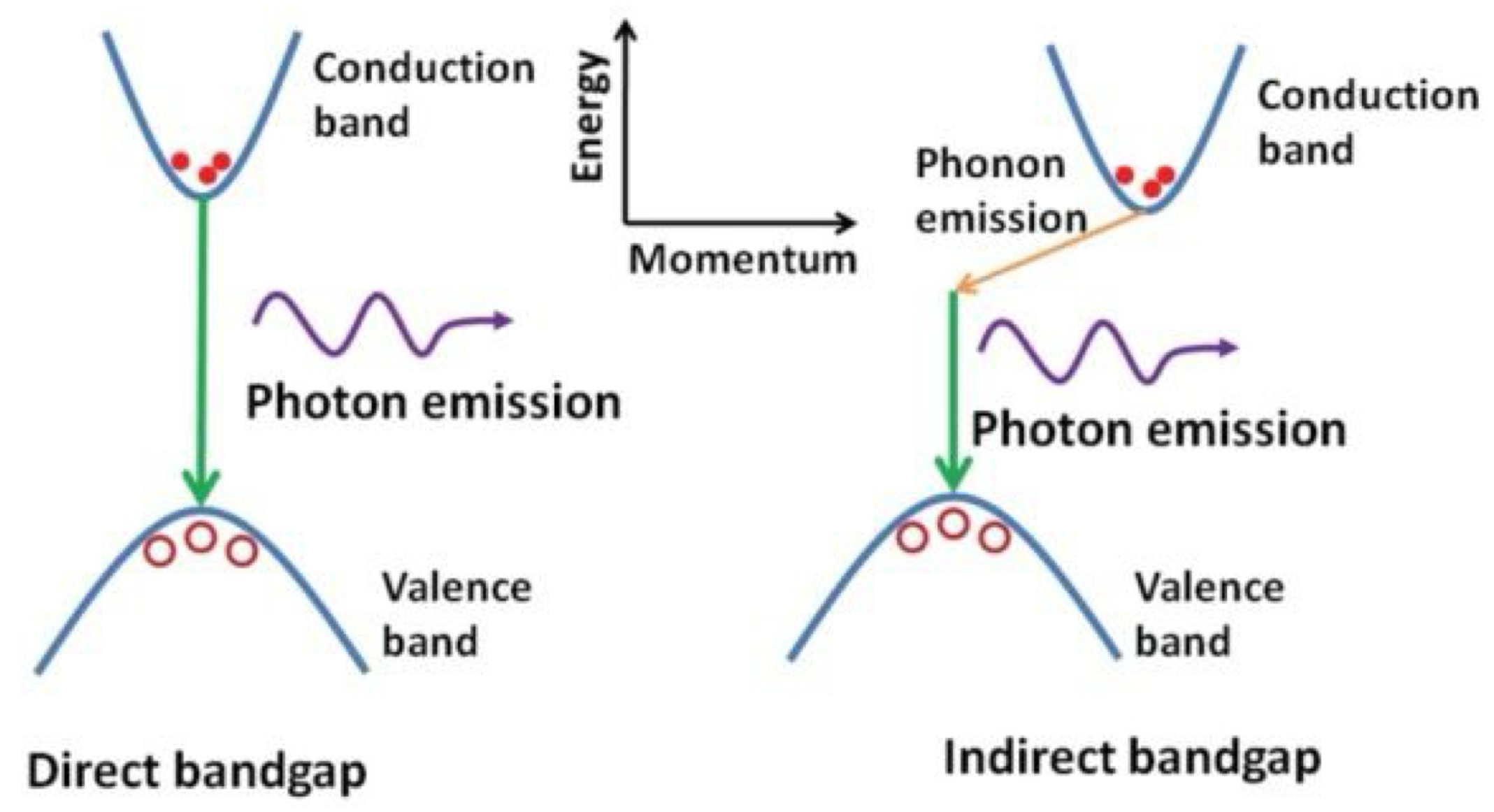
What is the difference between a direct + an indirect semiconductor, and why can only direct semiconductors be used for efficient LEDs?
direct: conduction band minimum + valence band maximum occur at the same momentum
electrons can directly drop from CB to VB + release its energy as a photon
efficiently produces light for LEDs
indirect: conduction band minimum + valence band maximum occur at different momenta
recombination requires the electron to also interact with a phonon + mainly releases heat instead of light (poor for LEDs)
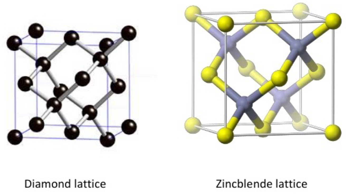
What is the zincblende lattice + how does it differ from the diamond lattice?
zincblende lattice: cubic (F-43m) crystal structure with tetrahedral coordination, where 2 different atoms alternate between positions
identical to diamond lattice, except diamond structure has only 1 type of atom (Si, Ge), while zincblende alternates between 2 types (Ga + As)
What can happen to a semiconductor’s light emission if a new element is added to its composition?
Can change the band gap energy, which shifts the emitted light’s wavelength + colour.
How does the size of a semiconductor’s band gap relate to the colour of light it emits?
larger band gap emits higher-energy, shorter-wavelength light (toward blue/UV)
smaller band gap emits lower-energy, longer-wavelength light (toward red/IR)
How can a single semiconductor family emit multiple colours of light?
By changing the ratios of its elements, the band gap can be tuned to produce different photon energies + therefore different emission colours.
How does T affect the efficiency of light emission in LEDs?
Higher T reduce efficiency because they increase non-radiative recombination, where energy is lost as heat instead of light.
What does a very large band gap tell you about the type of light a material can emit?
A very large band gap means the material can emit high-energy, short-wavelength light such as ultraviolet.
What is a direct-to-indirect band gap crossover?
The composition point where a semiconductor alloy changes from having a direct band gap (efficient light emission) to an indirect one (inefficient light emission).
Why is GaAs efficient for light emission but GaP is not?
GaAs has a direct band gap, so electrons + holes can recombine easily to emit photons
GaP has an indirect band gap that requires a phonon for recombination, reducing light output
What does tuning the phosphorus content in GaAs₁₋ₓPₓ allow us to control?
Lets us control both the efficiency of light emission + the wavelength (colour) of the emitted light.
Why are double perovskites useful in materials research?
they offer a way to replace toxic metals like lead, improve stability + tune optical or electronic properties
using 2 different metals allows fine control of the band gap energy, enabling better matching to the solar spectrum or desired emission wavelength
Why do most materials for LEDs + other electronic devices start as solid minerals, and why do they need to be heated during synthesis?
elements like Si, Ge, In + Ga naturally exist as stable oxides (such as sand), which are solid at room T
to use them in devices, they must be transformed into thin films or nanostructures to control light + electrical behaviour
this requires thermal processing (melting, vapour deposition) to reshape the solid materials into the desired nanoscale forms
Why might gallium be considered special among elements typically used in electronics?
It melts near room T, making it easier to process into nanostructures compared to other solid elements.
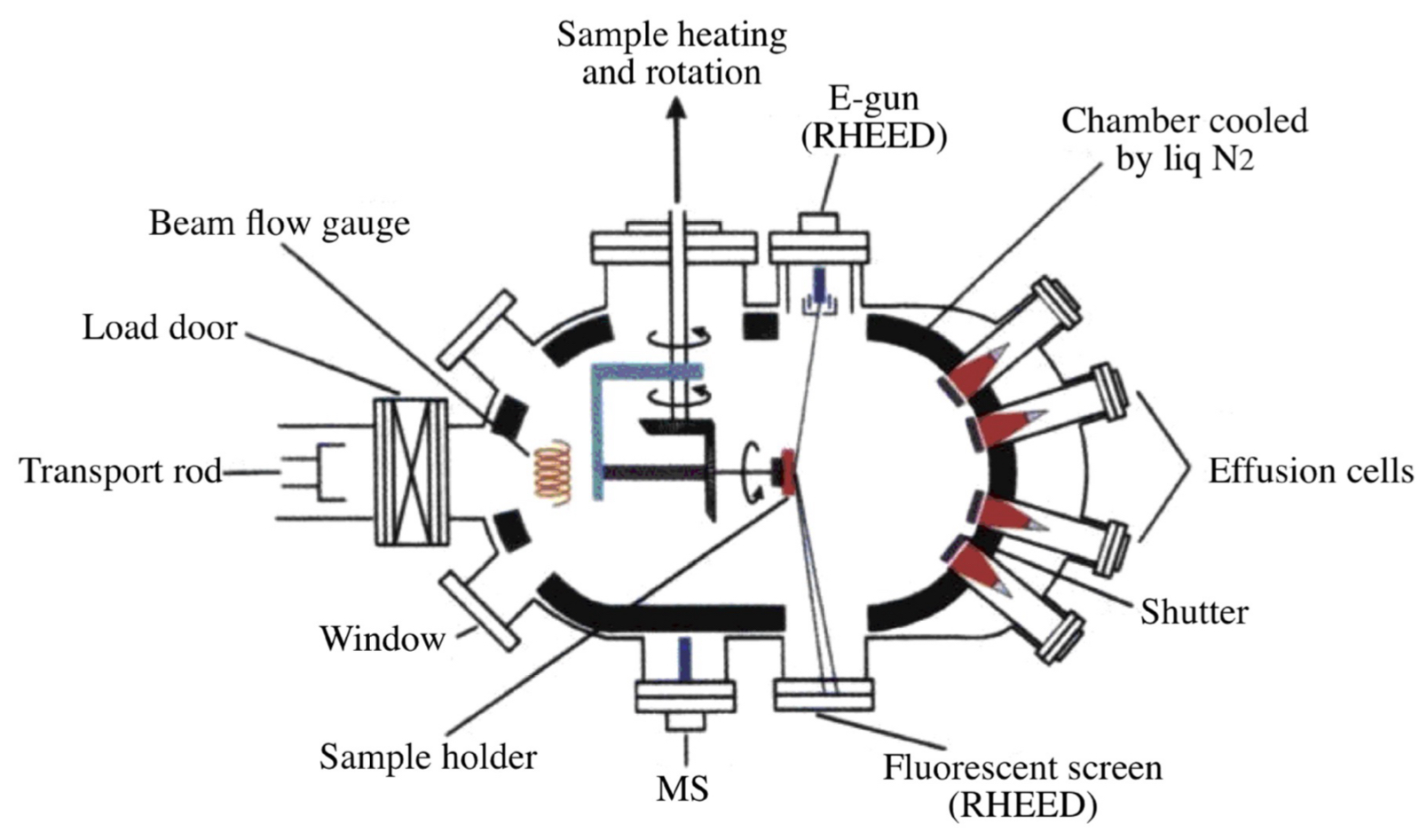
What is molecular beam epitaxy (MBE) + what are its main requirements and processes?
MBE: technique used to grow very thin, high-quality crystalline films by directing beams of heated atoms or molecules onto a substrate in an ultra-high vacuum environment
key requirements: clean room, ultra-high vacuum (UHV) chamber + heating systems
process:
materials are heated in effusion cells to produce atomic or molecular beams that travel toward the substrate
the substrate is heated + rotated for uniform growth, while shutters, an electron gun, mass spectrometer + fluorescent screen help monitor and control deposition
the chamber is cooled with liquid N to maintain vacuum stability
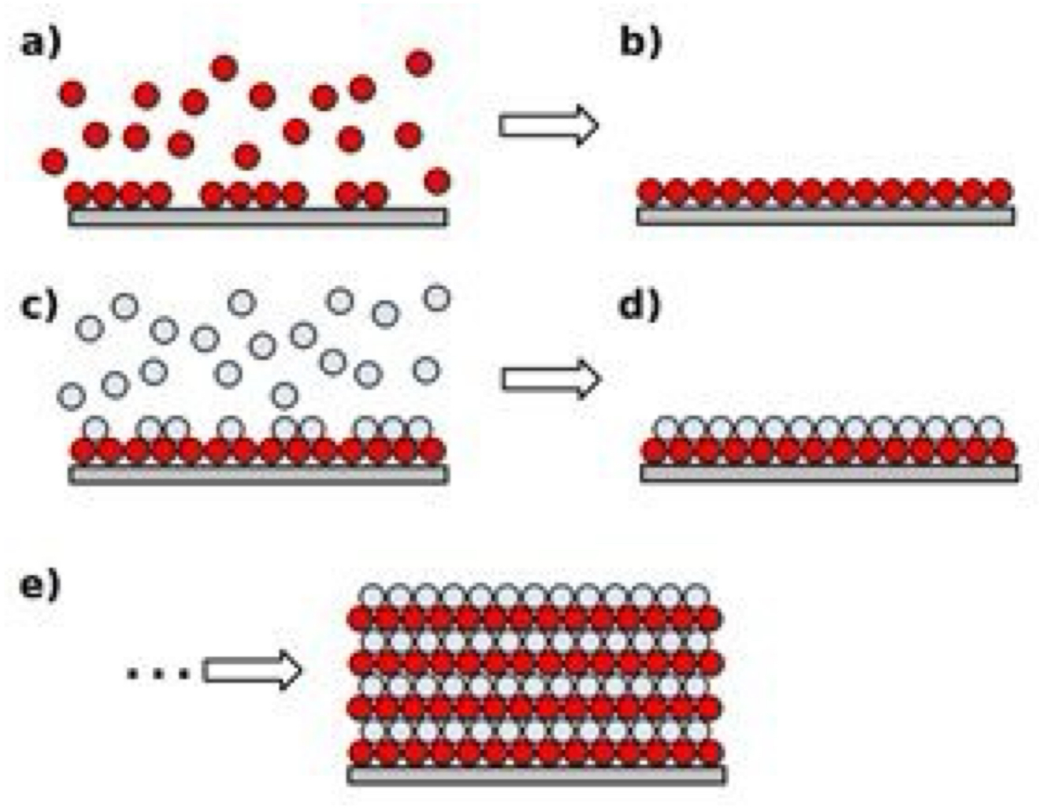
What is atomic layer deposition (ALD) + how does it work?
ALD: gas-phase chemical process used to create thin films with atomic-level precision
process:
exposes a substrate to alternating pulses of different chemical precursors that react one at a time in a self-limiting way
this ensures each reaction forms only one atomic layer before the next precursor is added
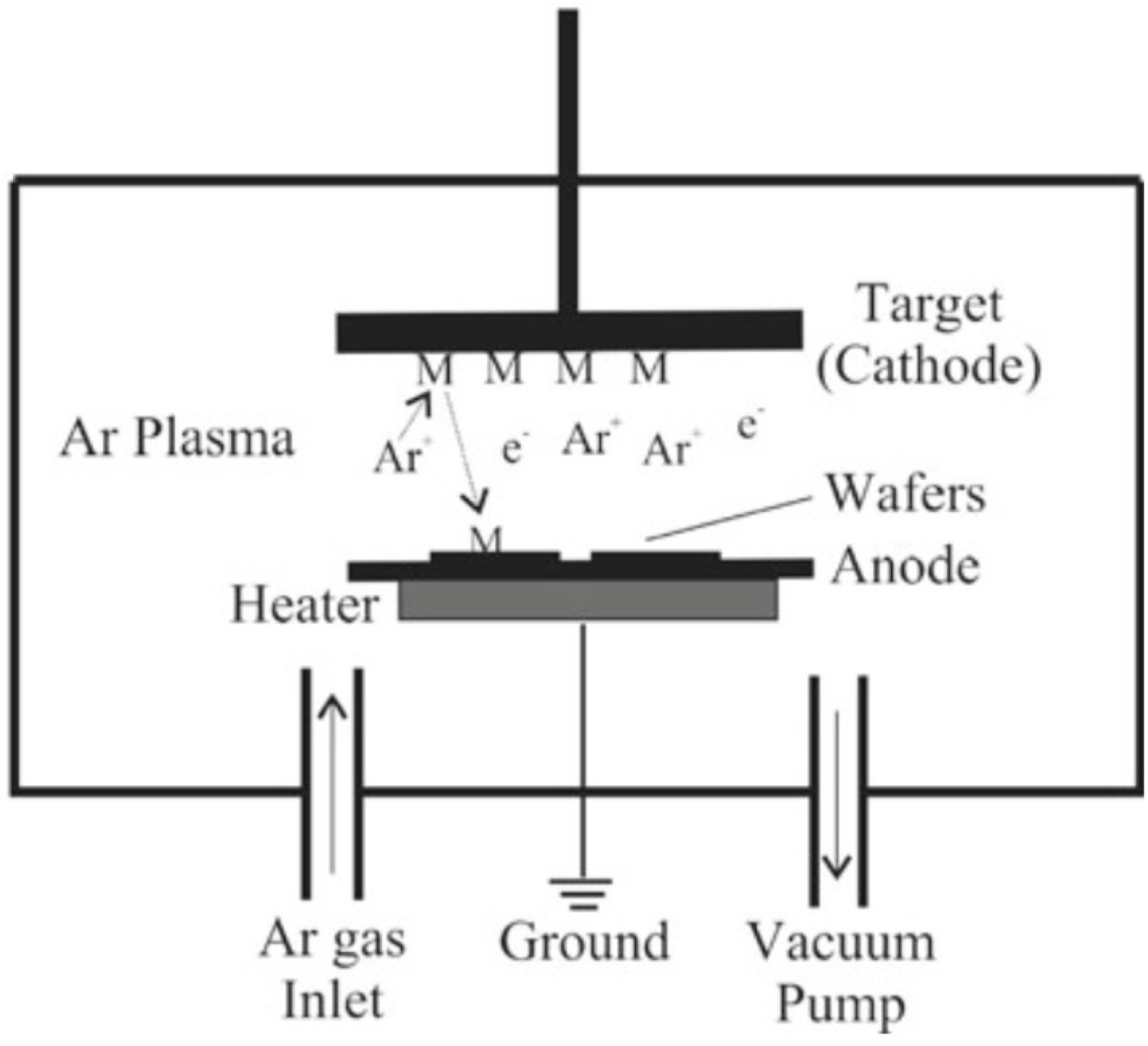
What is sputtering + how does it work?
sputtering: process where energetic ions (commonly Ar+) strike a solid material called the target, knocking off atoms from its surface
these ejected atoms (like tiny elemental bullets) travel through the chamber + land on a nearby substrate, forming a thin film coating
commonly used to deposit metals, oxides, or other materials with precise composition control
What is metal organic chemical vapour deposition (MOCVD) + how does it work?
MOCVD: technique used to create thin films
process:
vaporizes volatile metal-organic molecules, which are carried into a heated chamber
inside, these molecules decompose, leaving behind atoms that form a clean, uniform film on the substrate
the organic parts of the molecules ideally burn away cleanly
this process allows for precise control of film thickness + composition and is commonly used to grow semiconductor materials
Why are organic molecules used for electroluminescent devices + what were their initial limitations?
organic molecules are used because they…
have high photoluminescent quantum yields
are solution-processable at low T
can be synthetically tailored
allow flexible, thin, lightweight devices
initial limitations: being insulators, with low power conversion (~0.1% W/W) + moderate photon/electron efficiency (~5%)
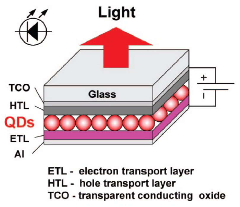
What semiconductor-like properties must molecules or polymers have to function in an OLED + how is the device structured?
must have a band gap, be able to be doped (n-type or p-type) + transport electrons and holes
device typically has a cathode, electron transport layer, emissive layer, hole transport layer, hole injection layer, anode + substrate to control charge flow and light emission
What is the basic structure of an OLED + how do the layers function to produce light?
cathode injects electrons + anode injects holes
electrons travel through the ETL + holes through the HTL to meet in the emissive layer
there, excitons (electron-hole pairs) form + emit light when they recombine
design principles include external quantum efficiency, brightness, thermal stability + lifetime
How do quantum dot LEDs compare to OLEDs in terms of structure + performance?
quantum dot LEDs have a similar structure to OLEDs with ETL, HTL + TCO layers
performance:
uses quantum dots as the emissive material, which have high internal quantum yields + size-dependent emission, but can have low efficiency + short lifetimes
What are the main challenges in using polyfluorene as a blue emitter in polymer LEDs?
degrades faster due to thermal, oxidative + morphological instability
this limits lifetime + reliability for devices like solar cells, plastic lasers
Why do polyfluorene polymers sometimes emit green light instead of blue?
Green emission arises from defects such as fluorenone units formed by oxidation, aggregation of polymer chains + excimer or other defect-related emissions.
What does conjugation influence?
absorption, brightness + colour
low conjugation → higher energy absorption → shorter wavelength (UV)
high conjugation → lower energy absorption → longer wavelength (visible)
How does modifying the chemical structure of a material influence its properties?
changes like increasing conjugation, adding bulky groups, or raising Tg can tune absorption, colour, brightness, thermal stability, aggregation + light propagation
this enables materials to perform in extreme environments or specific applications (solar cell, high-T lubricants)