4 - Scanning Electron Microscopy
1/18
There's no tags or description
Looks like no tags are added yet.
Name | Mastery | Learn | Test | Matching | Spaced | Call with Kai |
|---|
No study sessions yet.
19 Terms
What are the components of a scanning electron microscope?
Electron source/gun produces beam of e-. Typically W filament, LaB6, or field emission gun (FEG).
e- beam passes through the central column, which comprises condenser lens(es) [determines beam current that impinges on sample] and objective lens [determines final spot size of the e- beam].
Scanning coil used to deflect the beam in X-Y directions → raster scan over the sample surface.
Specimen chamber, hosts sample as well as a range of detectors, typically for secondary electron (SE), back-scattered electron (BSE), and X-rays. Typically under vacuum conditions.
How does the electron beam interact with samples?
Typically interested in SE (topography), BSE (composition), CL (composition), and characteristic X-ray (chemical composition).
Fluorescence and Bremsstrahlung important for background characterisation.
Secondary electrons: inelastically scattered from the emission of valence e-. Low energy.
Backscattered electrons: elastically scattered; high Z elements backscatter e- more strongly than low Z ones. High energy.
Characteristic X-rays: ejection of inner shell e- compensated for by e- in higher orbital dropping down → excess energy given off as X-ray.
Continuous X-rays: result from e- decelerating when travelling close to target nucleus → looses energy as X-ray photon.
What is the electron interaction volume equation?
R= (0.0276×E^1.67×A)/(ρ×Z^0.89 )
E = electron beam energy (keV)
A = atomic weight (g/mol)
ρ = density of target (g/cm3)
Z = atomic number of target
→ R increases with electron beam energy E
→ R decreases with target atomic number Z
What are secondary electrons?
SE images are based on the characteristics of the surface topography (roughness) of the specimen, and are not dissimilar to images observed by eye.
SE are e- with energies of 0 to ~30 eV, which originate from within the target specimen.
Target atomic number Z does not influence signal strength.
Most SE originate <100 nm from the specimen surface.
Divergence of primary beam within target is thus almost zero → image resolution ~ incident beam diameter.
How are back scattering electrons used in minerology?
• BSE imaging of polyphased material allows visualising different phases (e.g., minerals in a rock).
• BSE imaging of single phases allows visualising chemical zoning:
→ Mg-Fe in olivine
→ Trace elements (U, Th, REE) in zircon
What are characteristic x-rays?
Characteristic X-ray produced by electron transitions between bound electron orbits.
Removal of an inner electron is necessary for production of characteristic X-ray.
For characteristic X-ray line to be produced, incident electron energy E0 must exceed critical excitation energy EC required to excite the relevant shell.
Kα X-ray is produced due to removal of K shell electron, with L shell electron taking its place. Kβ occurs when K shell electron is replaced by electron from the M shell.
Lα X-ray is produced due to removal of L shell electron, replaced by M shell electron.
Mα X-ray is produced due to removal of M shell electron, replaced by N shell electron.
What is the critical excitation energy of characteristic x-rays?
Critical excitation energy EC = min. energy eject electron from atomic shell.
Also known as excitation potential and X-ray absorption edge energy.
With increasing atom size (increasing Z), EC required to excite any particular transition line also increases.
EC is higher than associated characteristic X-ray energy.
EC Ka ~ Σ(line energies) ~ Ka + La + Ma
What is overvoltage?
• Overvoltage U = E0/EC
→ ratio of accelerating voltage (gun) to critical excitation energy for selected line.
• Max. efficiency at ~2-3 times EC.
• Fe: min. accelerating voltage needed to excite Ka ~ 15 kV.
• U: min. accelerating voltage needed to excite La ~ 30 kV.
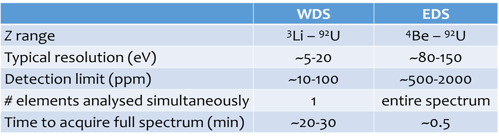
What is an Energy dispersive spectrometer (EDS)
• Solid-state detector (semiconductor).
• As each X-ray photon hits detector, small current produced.
• Records X-ray of all energies simultaneously.
• Low energy resolution, typically 80-150 eV wide.
→ good for broad qualitative characterisation of chemistry of samples investigated.
EDS allows producing X-ray element maps of whole sample → very useful for looking at their mineralogy.
Can combine several elements into composite X-ray map
How must samples be prepared for SEM and EPMA?
Secondary electrons
• Information on topography – no need to be flat.
• May need fixing to stabilise friable components.
• Sample typically glued to a stub.
Backscatter electrons and X-rays
• Need flat surface nicely polished to remove topographic effects.
• May need impregnating as for thin section preparation.
Interaction between the incident e- beam and target results in electric current developing on specimen surface. Unless target is a conductor (e.g., metal), electrical charges build up → apply thin layer (10’s nm) of conductive coating over the sample, typically C.
What is Electron Probe MicroAnalysis (EPMA)?
Electron source/gun produces beam of e-. Typically W filament or FEG.
Electron beam focused by coils, condenser and objective lenses, and apertures → beam typically ~1 μm Φ.
Scanning coil used to deflect the beam in X-Y directions → raster scan over the sample surface.
Detectors for secondary electron (SE) and back-scattered electron (BSE), and X-ray energy dispersive (EDS) and wavelength dispersive spectrometers (WDS).
High vacuum to limit interaction with gas molecules (~10-4-10-5 Pa).
What is Wavelength dispersive spectrometer (WDS)?
• Typically 4-5 WDS spectrometers with 1-4 diffracting crystals.
• Incoming X-ray dispersed by crystals, with a single wavelength diffracted to detector.
• Each detector records one wavelength at a time.
• Detector is gas-filled tube where gas is ionised by X-rays, yielding large multiplication factor.
• High spectral resolution, typically 5-20 eV.
→ high precision quantitative chemical analysis of chemistry of samples investigated.
How does Bragg’s law impact crystal type for WDS?
nλ = 2d.sin(θ) → Braggs’ law
• LIF, PET & TAP most common crystals.
• H-crystals: smaller circle radius, more limited range, but higher count rates.
• L-crystals: large analysing crystals for trace element analyses.
Compare EDS and WDS
Molybdenite (MoS2) EDS (yellow) and WDS (purple) spectra.
In EDS spectrum, Mo Lα line @ 2.293 keV severely overlapped by S Kα @ 2.307 keV.
These lines are clearly resolved in WDS spectrum. Also resolves S Kβ and Mo Lβ.
EDS is cheaper, quicker, but some interferences impossible to resolve, and detection limits are fairly high → qualitative overview.
WDS is more expensive and time consuming, but much better spectral resolution and detection limits → quantitative chemical analysis.
How is WDS spectra used to produce quantitative chemical data?
• Check for possible peak overlaps.
• Here want to quantify O Ka peak.
• Precisely position peak centre.
• Position background analysis positions on both side. Caution with interfering peaks.
• Decide on appropriate model to fit background – linear?
• Polynomial fit better here.
What equations are used for standardisation and corrections?
〖C'〗_unk=C_std×I_unk/I_std
Apparent concentration in unknown is equal to concentration in standard multiplied by intensity ratio of unknown/standard.
C_unk=〖C'〗_unk×F_unk/F_std
Real concentration in unknown is equal to apparent concentration in unknown multiplied by correction factor ratio of unknown/standard.
F=F_Z×F_A×F_F
Correction factor is function of corrections resulting from backscattering (Z), absorption (A), and fluorescence (F). Known as matrix correction ZAF.
We choose standards that are as similar as possible to the unknown to minimise the correction factor extrapolation → Funk /Fstd ~ 1.
What indicates a good analysis?
Totals: Having sum of all major elements analysed close to 100 wt.% suggests analysis is ok. Typically in range 98.5-100.5 wt.% for silicates and glasses.
Stoichiometry: calculated mineral stoichiometry from analyses makes sense (we’ll come back to this in practical).
What is stopping power correction?
• Incident electrons lose energy by interacting with inner shell electrons.
• Stopping power (= energy lost by electrons) drops with increasing Z.
→ higher number of X-rays produced in higher Z targets.
What is backscatter correction?
• Fraction of incident electrons backscattered increase with Z.
• Less incident electrons penetrate into targets with higher Z.
→ smaller number of X-rays produced in higher Z targets.