FE Exam - Electrical and Computer
1/214
There's no tags or description
Looks like no tags are added yet.
Name | Mastery | Learn | Test | Matching | Spaced | Call with Kai |
|---|
No analytics yet
Send a link to your students to track their progress
215 Terms
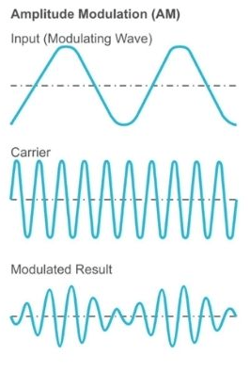
Amplitude Modulation (AM)
A modulating information signal varies the amplitude of a high-frequency carrier.
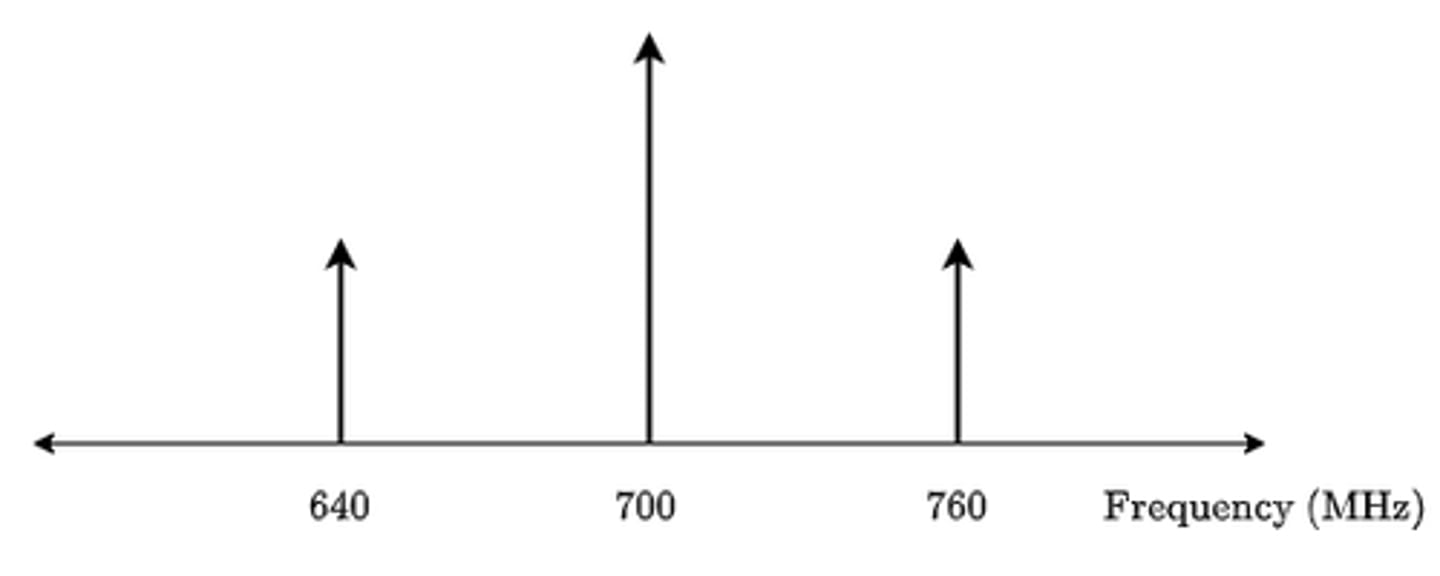
AM Frequency Domain Plane
The modulating signal is the message signal laid on top of the carrier signal.
The carrier signal is at 700MHz and the message signal is 60MHz with the two sidebands shown at 640MHz and 760MHz
How is the carrier signal modulated in FM?
A modulating information signal varies the frequency of the carrier.
What is the formula for carrier swing in FM?
Carrier swing = 2 x freq. deviation
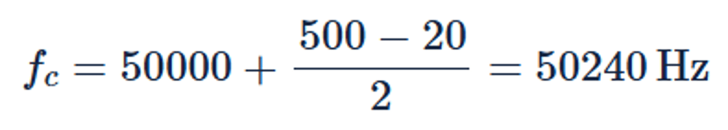
How is the carrier frequency calculated in FM?
Carrier frequency = (fmax-fmin)/2
What is the Modulation Index of an AM signal?
Ratio of peak voltage of the modulated signal and the unmodulated signal.
What happens when the peak voltage of the modulating signal exceeds the peak voltage of the unmodulated carrier in AM modulation?
Overmodulation occurs, resulting in distortion of the modulating (baseband) signal when it is recovered from the modulated carrier.
What is Frequency Division Multiplexing (FDM)?
A technique by which the total bandwidth available in a communication medium is divided into a series of non-overlapping frequency bands, each of which is used to carry a separate signal.
What are guard bands in FDM?
Guard bands are in between each communication band to avoid interference.
What is Time Division Multiplexing (TDM)?
Time division multiplexing is a type of multitasking where the controller swaps between different tasks or threads.
What is a frame in TDM?
A frame in TDM consists of one complete cycle of time slots in the multiplexing operation.
What does frame size represent in TDM?
In TDM, frame size indicates the amount of bytes of information sent per frame.
Simplex
There is a single channel and communication is in one direction only.
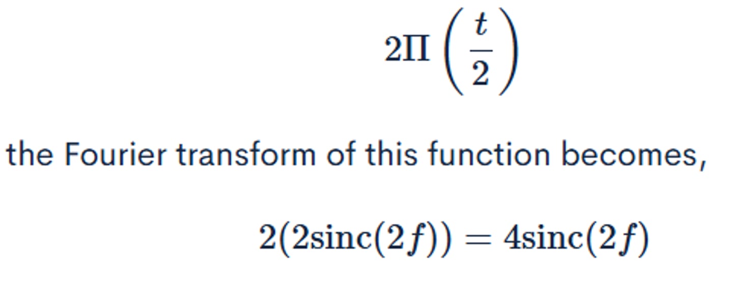
Rectangular Pulse Fourier Transform
Using the Fourier transform pair, substitute in the amplitude and total duration.
What is the purpose of a Band Pass Filter?
A Band Pass Filter can be used to suppress the lower and/or upper sideband, and the carrier.
How is the center frequency of a Band Pass Filter calculated?
The center frequency is calculated as the average value between the lower and upper ranges of the signal being modulated, with the carrier frequency added to this average.
How is the bandwidth of a signal determined in a Band Pass Filter?
The bandwidth in a Band Pass Filter is the difference between the lower 3dB point and upper 3dB point of the signal being modulated.
What is a parity bit?
A bit that acts as a check on a set of binary values.
What is the formula for frequency deviation?
D = (Δf)/fmax
What does Carson's Rule state?
Carson's Rule: BW = 2(Δf+fmax)
Transfer Function
H(ω)=Y(ω)/X(ω)
How does PCM convert analog to digital?
By sampling a message m(t) and digitizing the sample values with an A/D converter.
What is the formula for Channel Capacity (C) in terms of bandwidth (W) and signal levels (q)?
C = 2nW = 2Wlog_2(q)
Channel capacity is in bps
Nyquist Theorem
Sampling rate must be two times the bandwidth to accurately reconstruct the signal
Binary Phase Shift Keying (BPSK) Nyquist Capacity
BPSK is the binary form of PSK, where each signaling symbol can take on one of two values. Therefore, the quantization levels are q=2
B = 2W * log(q)
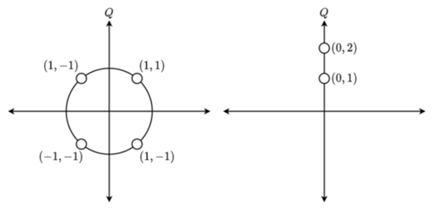
Modem constellation diagram
A way of representing digital signal modulation by shifts in the phase, amplitude, or frequency of the carrier signal.
Given two encoded coordinates (0,1) and (0,2). This is amplitude modulation because both points are the same angle from the positive x axis but are different distances away from origin (0,0)
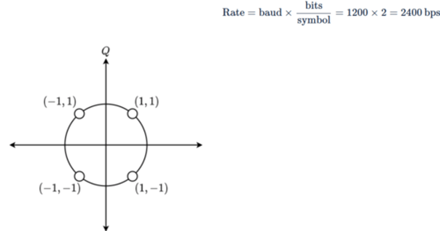
QPSK data rate
Rate = baud * bits/symbol
Baud is the number of symbols transmitted per second
QPSK encodes 2 bits/symbol
A baud rate of 9600 in serial communication is equivalent to:
9600 bits/sec
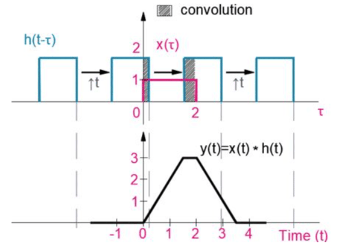
Convolution
Combining two signals to make a third signal
Z-transforms
Used to convert discrete signals (f[n]) in the time domain to a complex Z-domain (discrete version of the frequency domain). Similar to Laplace transform, Z-transform simplifies calculations.
![<p>Used to convert discrete signals (f[n]) in the time domain to a complex Z-domain (discrete version of the frequency domain). Similar to Laplace transform, Z-transform simplifies calculations.</p>](https://knowt-user-attachments.s3.amazonaws.com/5edb651c-e7e9-4827-8180-824a0e9a86a9.png)
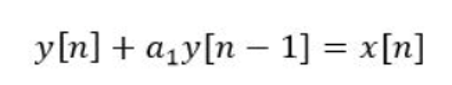
Difference Equations
Equation that uses the past inputs to determine the present input. For example, if you are at a time t = 3 seconds, then a difference equation for t = 3 seconds would be based on the values at t = 2 seconds and t = 1 seconds.
What is the purpose of analog filters?
To isolate signals with specific frequencies
Why are analog filters used in communication?
To allow multiple signals with varying frequencies to be sent over a transmission medium
Open Loop Transfer Function (OLTF)
G(s) = Y(s)/X(s)
Closed Loop Transfer Function (CLTF)
T(s) = Y(s)/X(s) = G(s)/(1+G(s)H(s))
Unity Feedback CLTF: T(s) = G(s)/(1+G(s))
Characteristic Equation
1+G(s)H(s) = 0
Natural Response
is when all applied inputs are set to zero for the characteristic equation
Match with form of general first or second order characteristic equation
Go to Diff Eq Section to determine solution
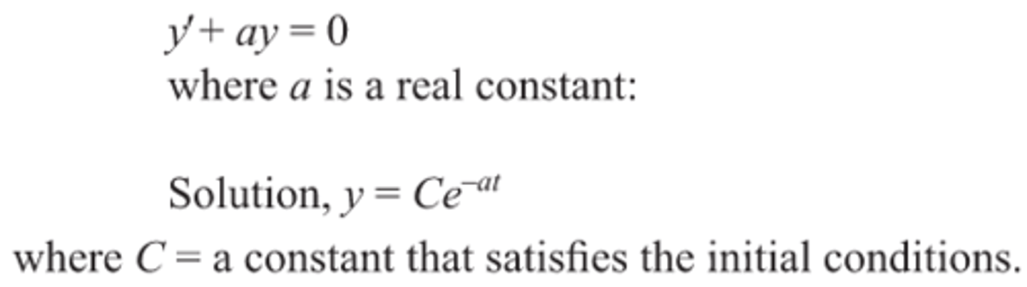
First order linear differential equation general solution
Use the characteristic equation to identify the order of the diff eq
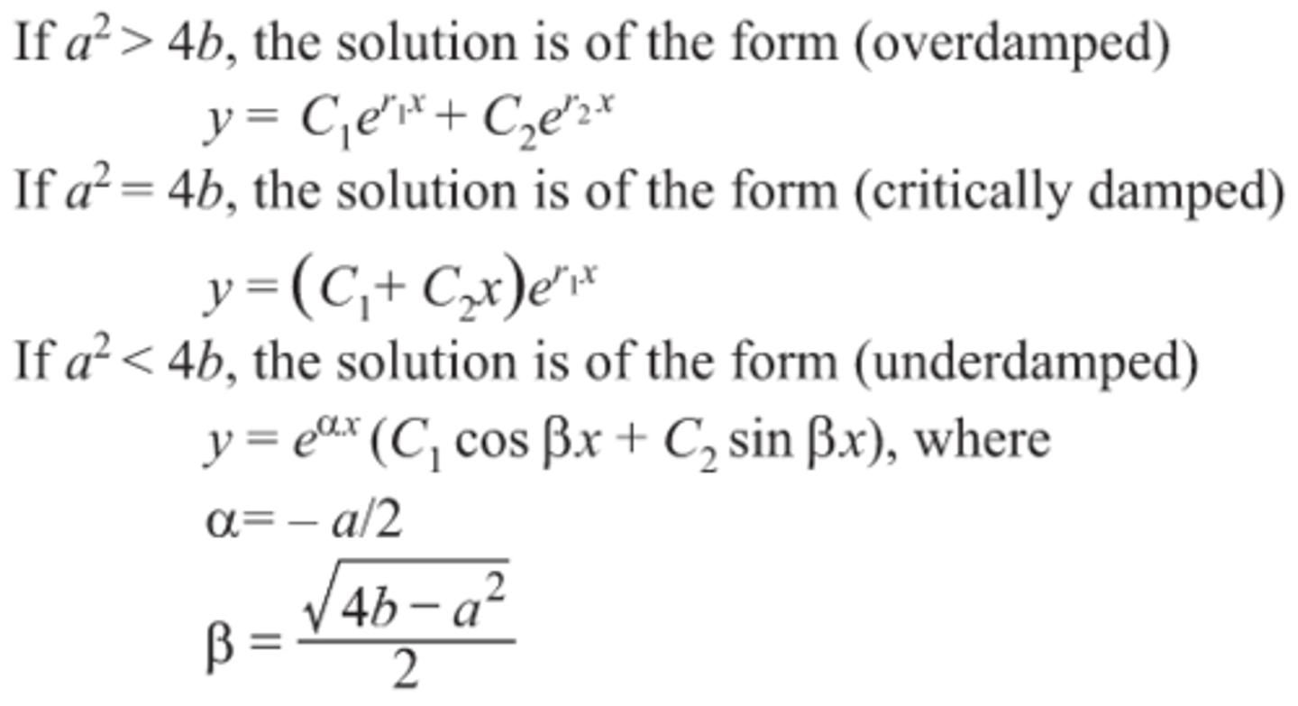
Second order linear differential equation general solution
Use the characteristic equation to identify the order of the diff eq
First and Second Order Control Systems
Use the CLTF H(s) = Y(s)/R(s) to analyze response parameters
Final Value Theorem (FVT)
DC Gain, K: lim t→∞ f(t) = lim s→0 sF(s)
F(s) can be an OLTF or CLTF
System input
Impulse, R(s) = 1
Unit Step, R(s) = 1/s
Ramp, R(s) = 1/s^2
Parabolic, R(s) = 1/s^3
Function of E(s)
E(s) = R(s) - Y(s) = R(s)/(1 + G(s))
Steady State Error, e_ss
The difference between the input and the output of a system after the natural response has decayed to zero.
Depending on the input and the system type, e_ss can be determined using the DC Gain equation and the steady-state error analysis table.
System Type
Number of poles in the system (the order of s in the denominator)
T = 0, no poles at origin
T = 1, one pole at origin
T = 2, two poles at origin
Poles and Zeros on Bode and Phase Plots
Read the bode plot one division at a time from left to right.
If the slope changes to be more negative, this is a pole
If the slope changes to be more positive, this is a zero
Phase plot will show a corresponding positive or negative phase shift
Magnitude of a Transfer Function
20log(H(s)) gives the magnitude response K
H(s) is the multiplicative constant * pole
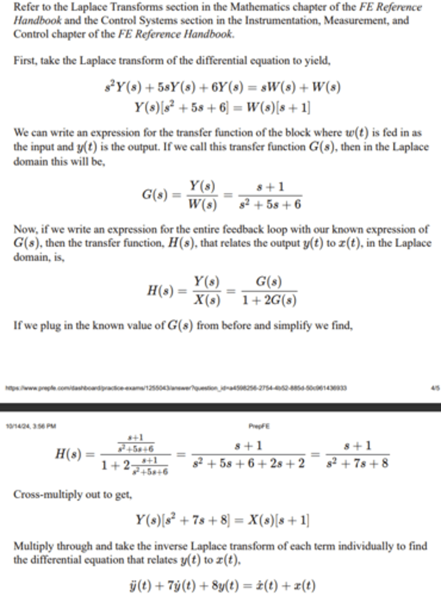
Laplace Transform of a Differential Equation
1. Convert dots to s terms
2. Factor both sides of the equation and rearrange to get the transfer function (output/input)
3. Write the CLTF. H(s) = G(s)/(1+H(s)G(s)).
4. Plug in the known value for G(s), solve and simplify to get the final CLTF.
For a unity feedback control system model, the steady-state error is most nearly defined as:
The difference between the commanded (input) value R(s) and the output value from the plant, Y(s).
Qualifying Criteria for Stability (Routh-Herwitz)
I. No missing terms, coefficient can not equal 0
II. No negative coefficients
III. No imaginary coefficients
Criteria for a system to be stable
For a bounded input there must be a bounded output and that the system is asymptomatically stable, which means that in the absence of an input, the output tends to zero.
Given the characteristic equation, how do you solve for the value of K that makes all the roots of the equation real?
Quadratic formula
Discriminant must be >= 0
Solve for K
Bandwidth of a spectrum
Bandwidth (Δf) is defined as the highest frequency present in the signal minus the lowest frequency present in the signal. Solve for frequency of the wave and multiply by Δf.
f=c/λ
BW = Δf=(Δλ/λ)×(c/λ) = (cΔλ)/λ^2
Phase velocity of a plane wave
v_p=ω/β
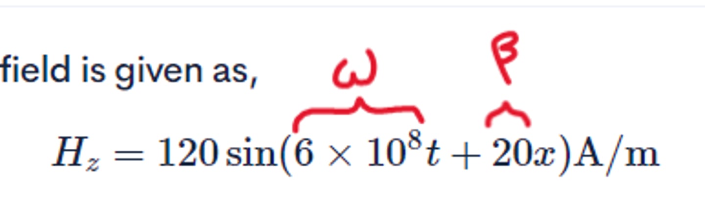
Frequency of a plane wave
f = ω/2π
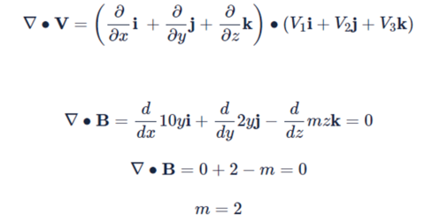
A magnetic field has the vector field B =10yi+2yj−mzk. The constant "m" is most nearly:
Calculate the divergence and set the expression equal to zero.
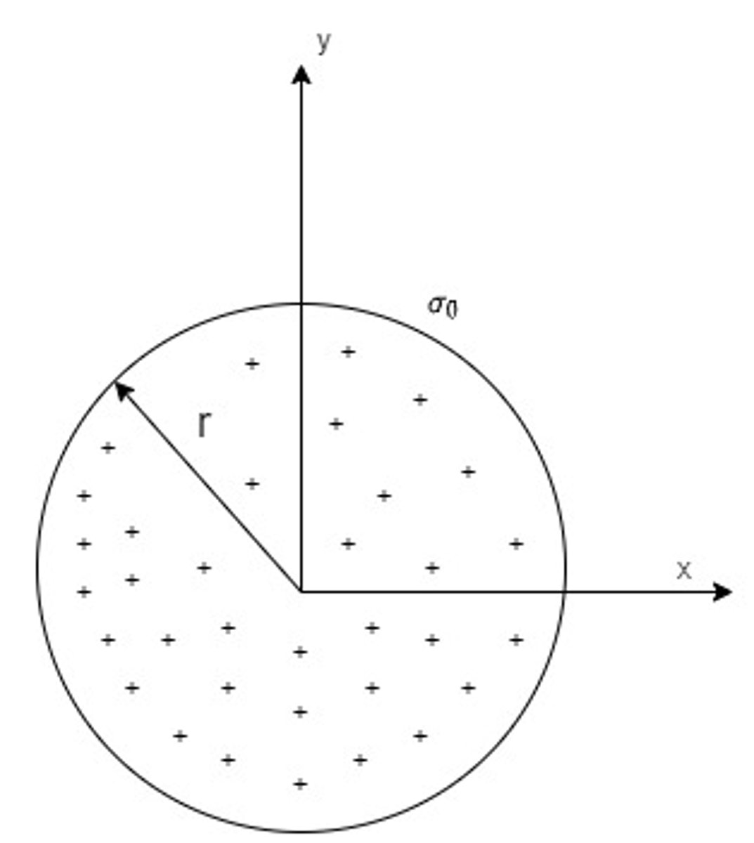
Find the total charge contained on the surface of a disk with radius r that has a uniformly distributed surface charge, σ0, on the surface of the disk, as shown in the figure.
π(r^2)(σ0)
Area of circle: A = πr^2
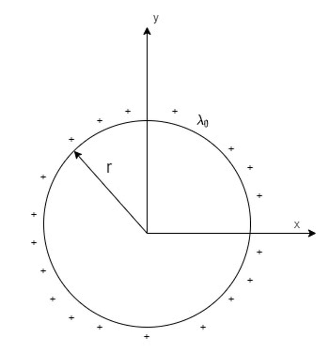
Find the total charge contained inside a ring with radius r that has a uniformly distributed charge, λ0, on the surface of the ring, as shown in the figure.
2πr(λ0)
Perimeter of a circle: C = 2πr
Find the total charge contained inside a sphere with radius r that has a uniform volume charge density, ρ0.
(4/3)π(r^3)ρ0
Electric Flux (Φ)
Represents the number of electric field lines passing through a closed surface. It depends on the strength of the electric field and the surface area and is defined as a dot product between the electric field and the area from which the electric field or electric line of forces are passing through.
Φ = E·ΔA = EΔA cosθ
Gauss' Law
The total electric flux through a closed surface is proportional to the total charge enclosed by that surface.
ΦE = (Qenclosed) / ε0
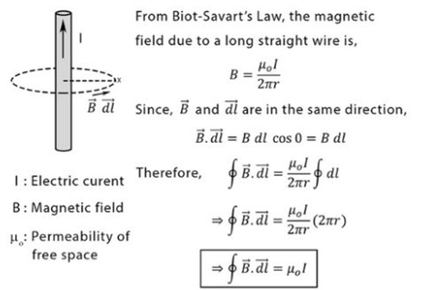
Ampere's Law
Relates the magnetic field around a closed loop to the total current enclosed by the loop.
∮B · dl = μ0 * I_enclosed
BL = μNI
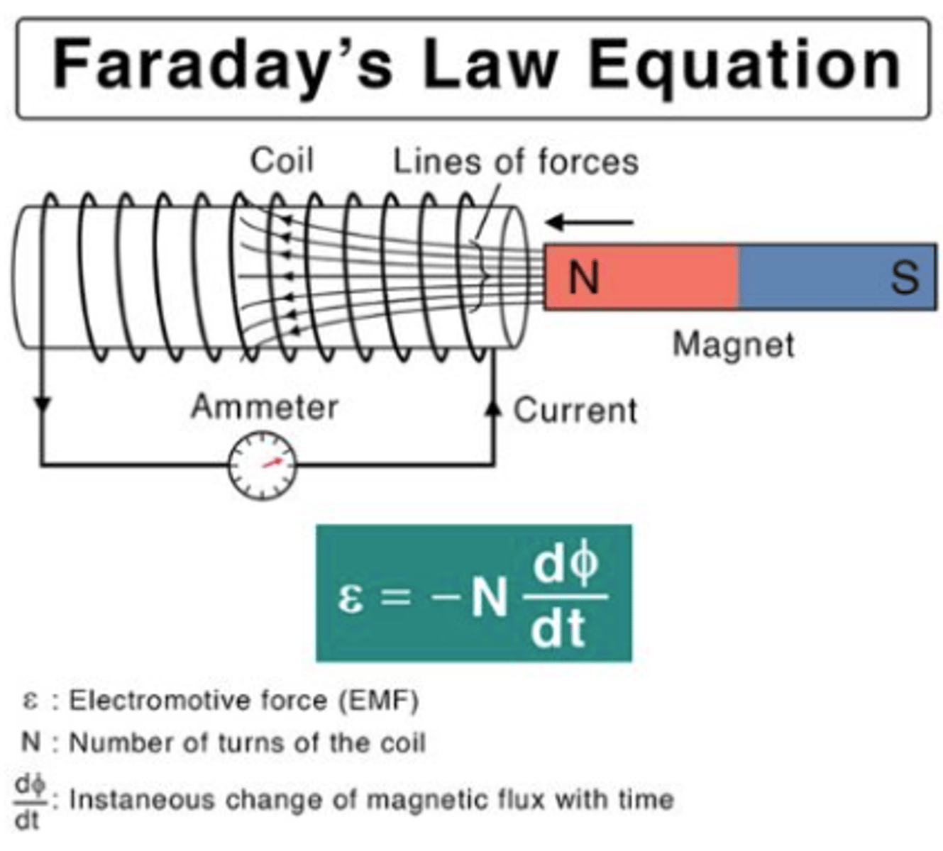
Faraday's Law
A changing magnetic field through a wire loop induces an electromotive force (EMF) and, consequently an induced current. The induced current flows in a direction that opposes the change in the magnetic field, as described by Lenz's Law.
EMF = -dΦB / dtS
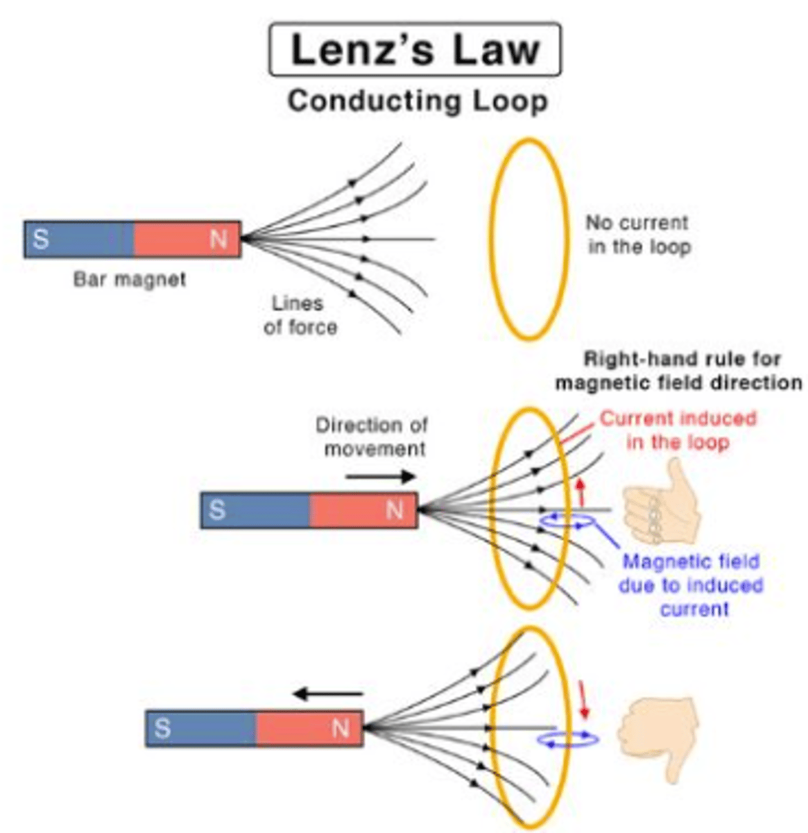
Lenz's Law
The direction of the induced current in a closed loop is such that it opposes the change in magnetic flux that produced it.
Gauss' Law for Electric Fields
∇ · E = ρ / ε₀
This equation relates the electric field (E) to the electric charge density (ρ) and the electric constant (ε₀). It states that the electric field divergence is proportional to the charge density.
Gauss' Law for Magnetic Fields
∇ · B = 0
This equation states that the magnetic field (B) has no sources or sinks. The magnetic field divergence is always zero, indicating no magnetic monopoles.
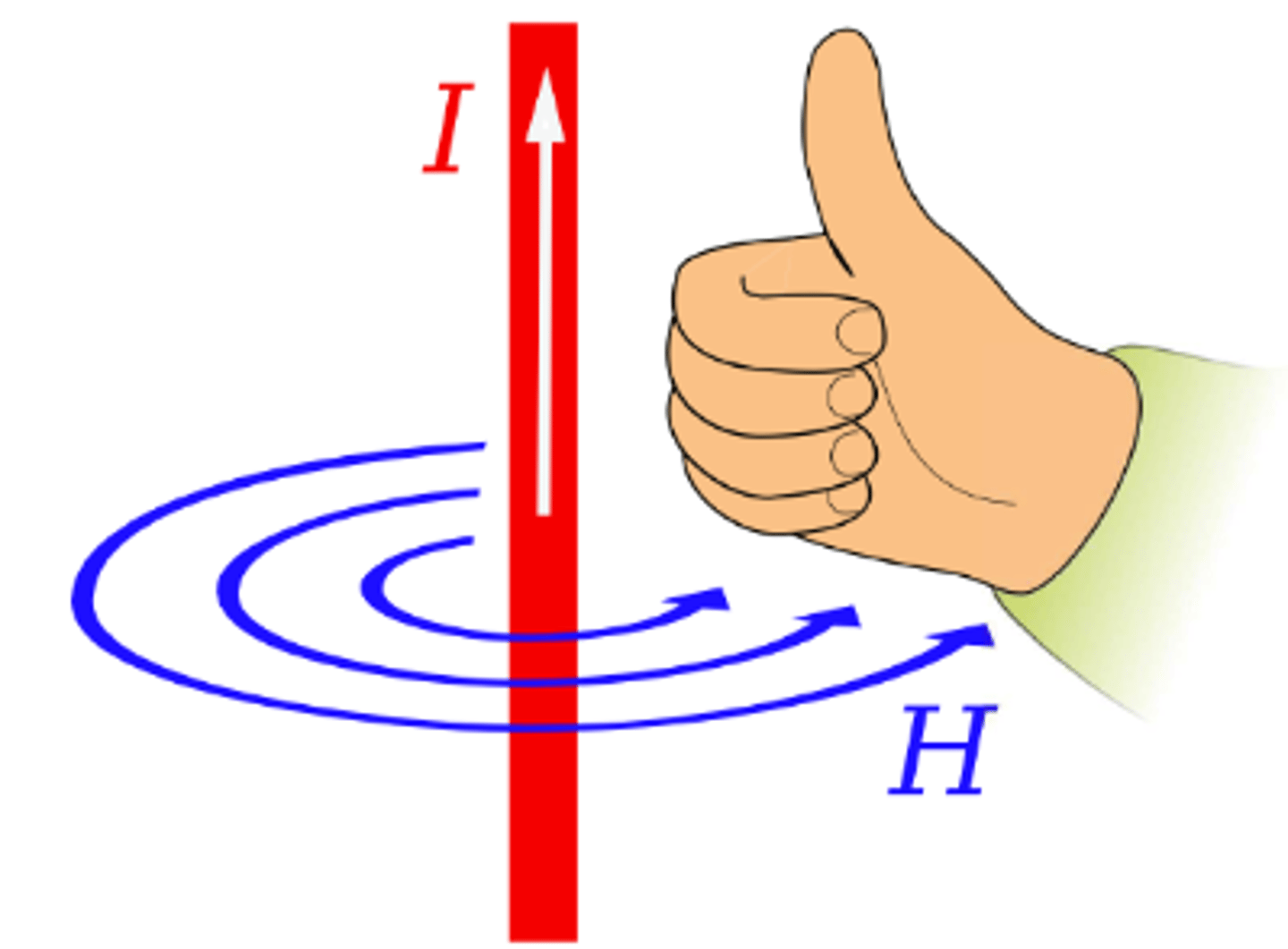
Magnetic Field Strength, H
H = B/μ = I/2πr
Magnetic Flux Density, B
B = Φ/A
A is cross-sectional area of a transformer
Force, F, in a Uniform Magnetic Field, B
F = IL x B

Propagation delay
Signals traveling through transmission lines experience a finite propagation delay. This delay is a function of the line's length and propagation velocity (typically a fraction of the speed of light).
Reflections
When signals encounter impedance mismatches along the transmission line, they can reflect back towards the source. These reflections can lead to signal degradation and must be managed to ensure proper signal transmission. (V+ is incident and V- is reflected. d=0 at the load)
Losses
Transmission lines exhibit both resistive and dielectric losses. Resistive losses are due to the line's resistance, while dielectric losses are caused by the insulating material surrounding the conductors. These losses can result in signal attenuation.
Impedance matching
Transmission lines have a characteristic impedance (Z0), which depends on their physical parameters. Matching the source and load impedances is essential to minimize reflections and maximize power transfer (ZL = Z0)
A 25mH inductor is in series with a 300Ω resistor. If the energy stored in the coil at t=0 is 1μJ, find the magnitude of the current at t=0.
E=(Li^2)/2
Energy Gap (Eg)
The amount of energy required to initiate carrier movement through a semiconductor.
Eg = E_conductance band - E_valence band
Activation energy, Q = Eg
Intrinsic n-type, Q = Eg/2
Extrinsic n-type, Q = Eg - Ed
Extrinsic p-type, Q = Ea
Doped n-type
Doped with donor atoms to give it an abundance of negative carriers. Na = 0, n >> p, p≈0; Nd ≈ n
What is the charge neutrality relationship for doped n-type materials?
Na + n = Nd + p, where Na = 0 and n >> p (p≈0), resulting in n ≈ Nd.
Doped p-type
Doped with acceptor atoms to give it an abundance of positive carriers. Nd = 0, p >> n, n≈0; Na ≈ p
What is the charge neutrality relationship for doped p-type materials?
Na + n = Nd + p, where Nd = 0 and p >> n (n≈0), resulting in p ≈ Na.
Equilibrium Carrier Concentration
(p)(n) = ni^2
An undoped semiconductor is electrically neutral, so intrinsic semiconductors have equal numbers of electrons and holes. Therefore, p = n = ni
Concentration of holes in n-type material
According to equilibrium carrier concentration [(p)(n) = ni^2] and since n ≈ Nd for p-type, p = (ni^2)/Nd
Concentration of electrons in p-type material
According to equilibrium carrier concentration [(p)(n) = ni^2] and since p ≈ Na for p-type, n = (ni^2)/Na
Conductivity
Depends on the mobilities and concentrations of the carriers (σ=1/ρ).
When the n >> p, σ = q(nμn+pμp) ≈ q(nμn)
Drift current
J = σE
J = q(nμn+pμp)E
Current
Electric current i(t) through a surface is defined as the rate of charge transport through that surface.
i(t) = d[q(t)]/dt
Constant current is written as I.
Current density is defined as J = I/S
Voltage
Potential difference, V, is equal to the work required to move one unit charge from one point to the other.
Resistance
A material's opposition to the flow of electric current.
R = ρL/A
Rsc = 0, Roc = ∞
Ideal Capacitor
Zc = 1/jωC = jXc
Voltage lags current by 90
Ideal Inductor
Zl = jωL = jXl
Current lags voltage by 90
Ideal Resistor
ZR = R
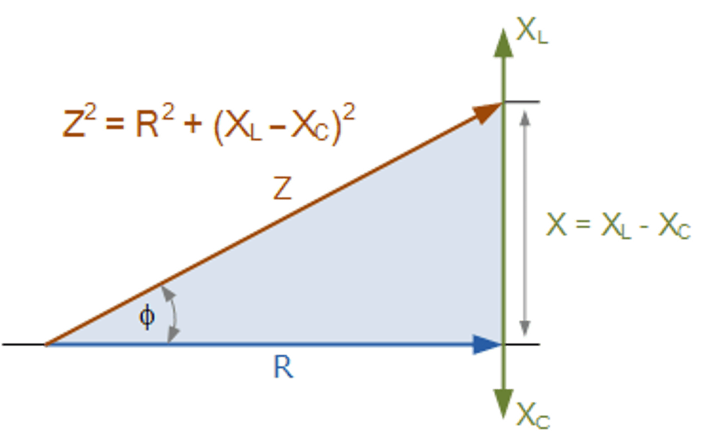
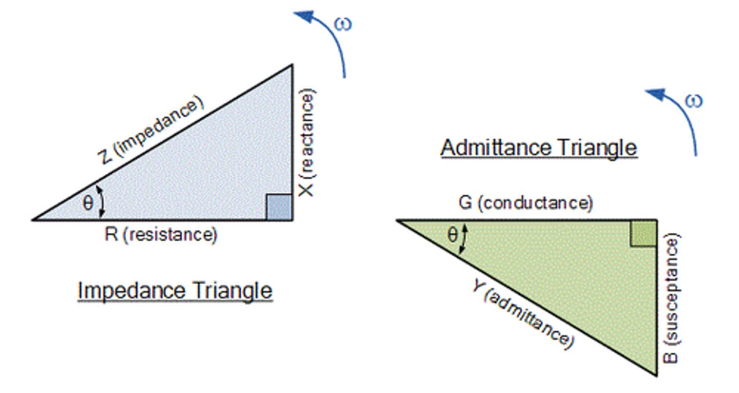
Impedance
Z = V/I
Z = R + jX
Z^2 = R^2 + (Xl - Xc)^2
Z = sqrt(R^2 + (Xl - Xc)^2)
Ohm's Law with Impedance
Z = V/I (max or effective values)
Find reactance (X) of the active component, then convert to Z and solve
Admittance
Y = 1/Z = I/V
Y = G - jB
Y^2 = G^2 - (Bc - Bl)^2
Y = sqrt(G^2 + (Bc - Bl)^2)
Series Circuits
I = I_R1 = I_R2 = I_R3
Req = R1 + R2 + R3
Veq = V1 + V2 = I * Req
V_R1 = (R1/Req) * Veq
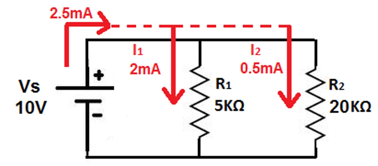
Parallel Circuits
V = V_R1 = V_R2 = V_R3
1/Req = 1/R1 + 1/R2 + 1/R3
I_R1 = (R1/Req) * I
Ieq = I_R1 + I_R2 + I_R3
DC Circuit Power
P = IV = I^2R = V^2/R
Sources and Sinks: must have a sign difference to denote
Ohm's Law
V = IR
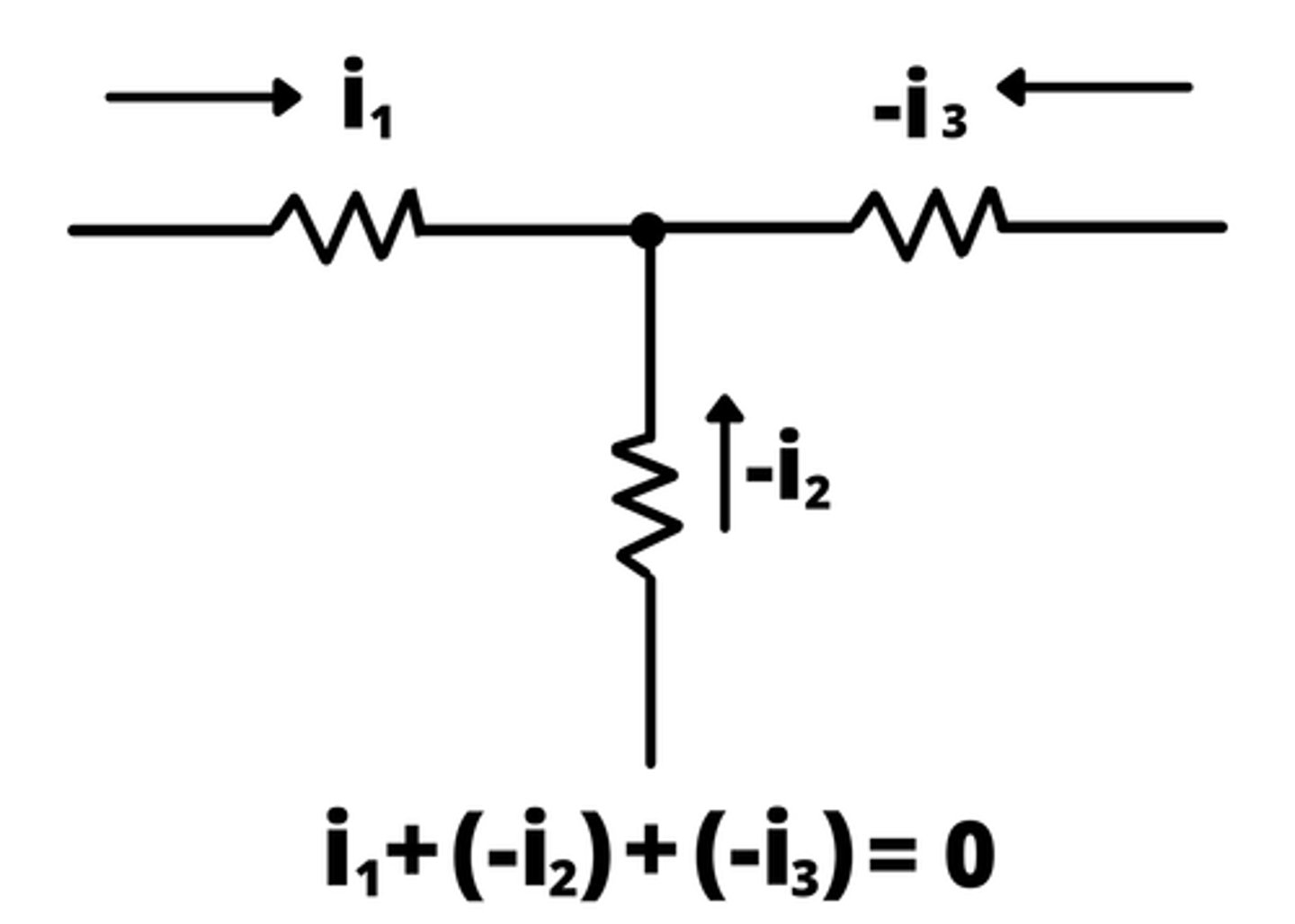
Kirchoff's Current Law (KCL)
Sum of Currents In = Sum of Currents Out
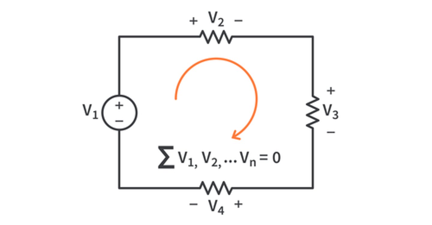
Kirchoff's Voltage Law (KVL)
Sum of Voltage Rises = Sum of Voltage Drops
Current Divider Circuit
I_R1 = I_1* (R2/(R1 + R2))
I_R2 = I_1 * (R1/(R1 + R2))