Devices (BJT)
1/15
There's no tags or description
Looks like no tags are added yet.
Name | Mastery | Learn | Test | Matching | Spaced | Call with Kai |
|---|
No study sessions yet.
16 Terms
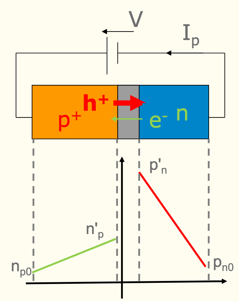
What are the concentration gradients for minority carriers in a forward biased p+n diode?
Upward slope for electron minorities, downward slope for hole minorities. Hole minority is placed much higher due to large hole flux from p+ region
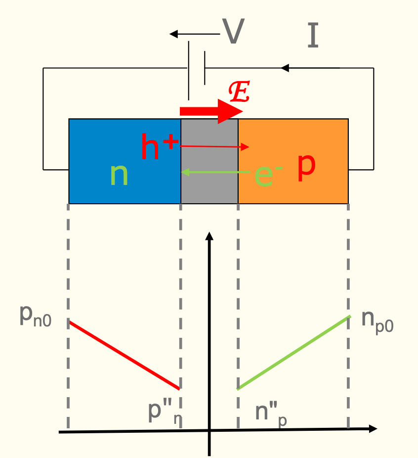
What are the concentration gradients for minority carriers in a reverse biased np diode?
Downward slope for hole minorities, upward slope for electron minorities. This is due to minority carriers drifting across the junction, so at the junction there is few carriers left.
What is I(E) equal to?
I(B) + I(C)
What is I(C) equal to?
I(pBC)+I(nBC)
(roughly) I(pEB) or I(nEB)
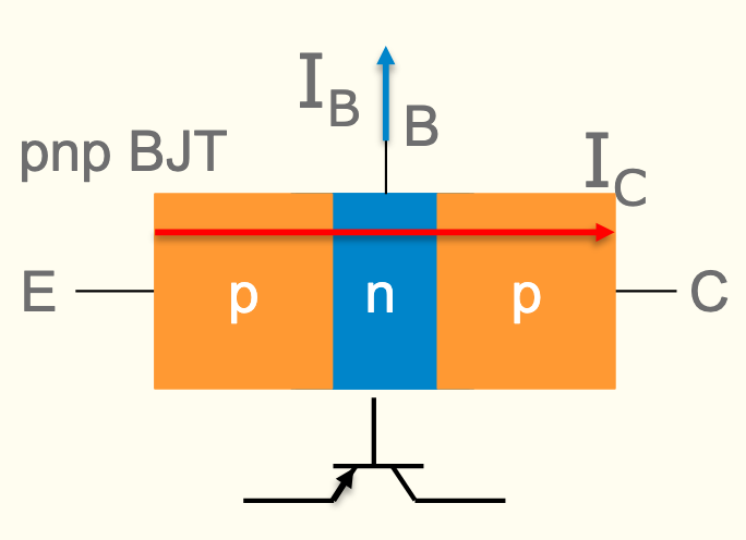
The sign for pnp BJT?
upward arrow (emitter)
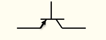
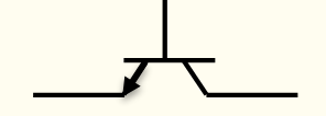
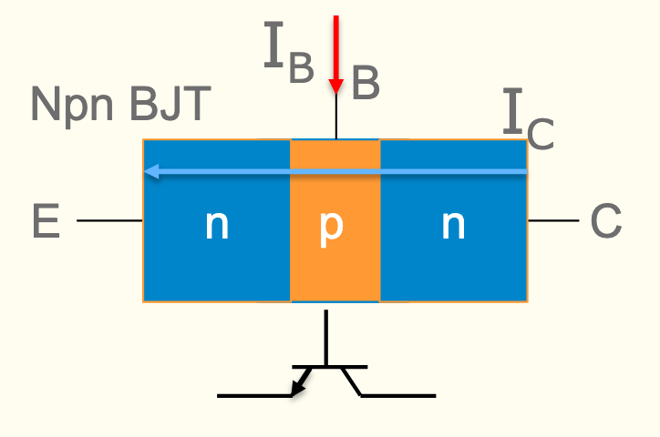
The sign for npn BJT?
downward arrow (emitter)
Direction of base current for pnp?
upwards (remember electrons are injected into n-type, and electron current direction is reverse of flux)
Direction of base current for npn?
downwards (remember holes are injected into p-type, and hole current direction is the same as flux)
Current gain?
β = I(C) / I(B)
Emitter injection efficiency
Ɣ = I(C) / I(E) = I(p) / (I(p) + I(n))
(for pnp)
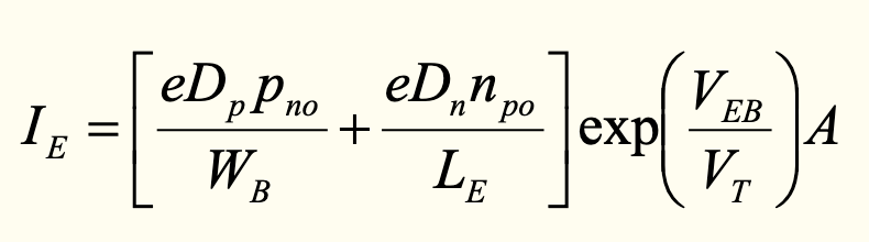
What is the equation for emitter current (in terms of exponential)?
Refer to PN equation, it is similar but not the same
Forward active mode
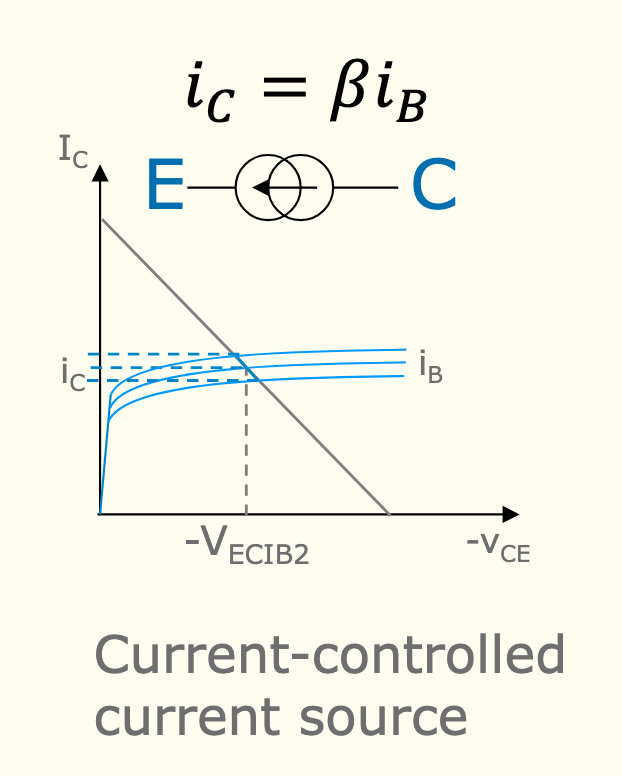
when BJT is in saturation, normally happens with common emitter and common base setups (constant current source)
Difference between common emitter and common base?
I(C) is plotted as a function of -V(EC), where the height of the function represents I(B), this is for common emitter.
I(C) is plotted as a function of -V(BC), where the height of the function represents I(E), this is for common base
(basically, we observe voltage of between the common “XXXX” and the collector)
Base width modulation
a non-ideal effect in BJTs that occur when V(BC) changes.
a change in V(BC) results in depletion width change (for the reverse bias junction), leading to a change in effective base width)
w(B) - w(n)*V(BC) = effective base width (original is w(B))
for a standard, non AC BJT, if there is base width modulation, this is modelled as a series resistor and the constant current source (current controlled current source)
Early voltage (V(A))
a resulting "extrapolation” that occurs due to base width modulation
base width modulation → thinner base → less recombination than usual → more carrier injection than usual in collector current → non-flat forward active mode (linear line upwards)
the non-flat lines all extrapolate to a point on the voltage axis (early voltage)
this early voltage represents the “theoretical voltage” required to bring the new non-ideal collector current to 0
Small signal equivalent
when we have an AC (typically through the base), we can just model the resulting collector current as an AC “result”
this entails a small variation of a collector current (if it was DC), and taking a small lower and upper bound version of it
instead of a series resistor for base-width modulation, there is a parallel resistor (parallel to current source)