Digital Electronics Ch. 3 "Introduction to Nonlinear Circuit Elements"
1/14
Earn XP
Description and Tags
Introduction to the properties of semiconductors, diodes, and transistors.
Name | Mastery | Learn | Test | Matching | Spaced |
|---|
No study sessions yet.
15 Terms
Piecewise Modeling
The method used to analyze circuits containing non-linear devices. It is an approximate solution that generally includes linear representations of device behavior in limited regions of operation.
Non-Linear Device
A non-linear circuit element has v-i characteristics that cannot be expressed in the simple form of a linear equation. (Example: diodes and transistors)
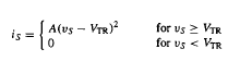
Square-Law Device
A square-law device is an electronic component whose output current is proportional to the square of the input voltage. It models the behavior of a real device called field-effective transistors.
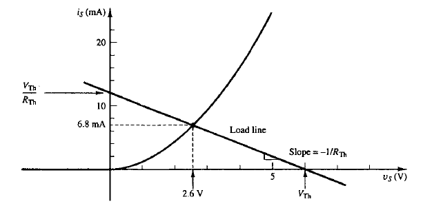
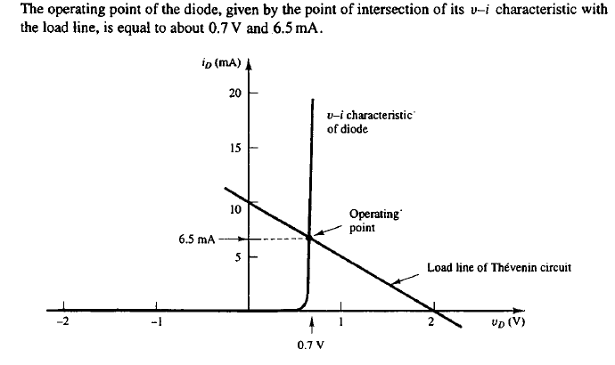
Load Line / Operating Point
The plotted v-i equation of a Thevenin circuit is called a load line. The load line can be drawn graphically over the v-i characteristic of any element to find the operating point.
Holes
When an electron is thermally excited outside of its covalent bond, it leaves behind a singular vacancy called a hole. The result is a positive charge.
Donors & N-Type Semiconductors
Donor atoms have one extra electron in their outer shell. The donor ion contributes an extra mobile electron, which is free to move about the crystal. The donor ion core leaves behind a net positive charge. A doped semiconductor with an abundance of free electrons is called an n-type semiconductor.
Acceptors and P-Type Semiconductors
Acceptor atoms have one less electron in their outer shell. The acceptor gains an electron and a net immobile negative charge. The adjacent atom loses an electron, creating a net positive charge. A doped semiconductor with an abundance of holes is called a p-type semiconductor.
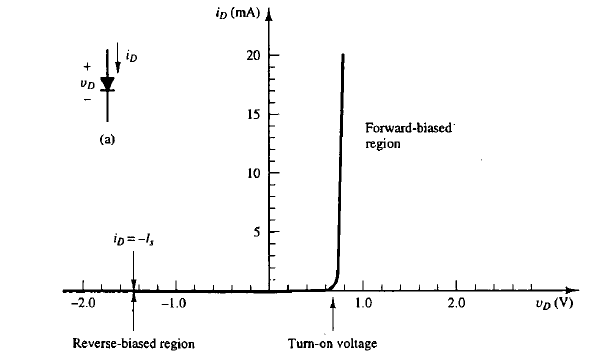
PN Junction Diode
A diode that is formed by the physical boundary of n-type and p-type materials
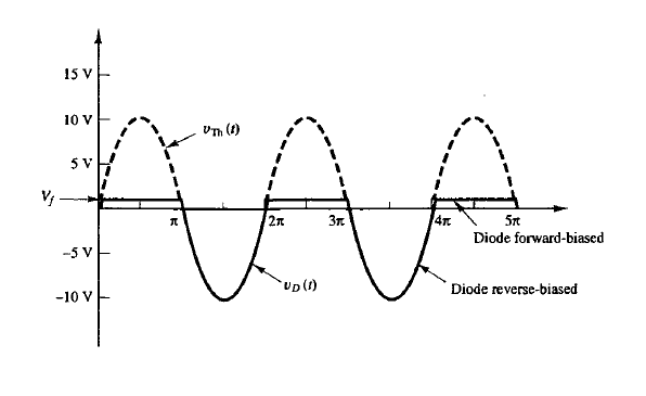
Reverse Biased
Occurs when the diode’s operating point is in the horizontal portion of its v-i characteristic, where vD is negative. The diode is said to be in its “off” state. No current will flow.

In a PN Junction, or Diode, current will flow when ….
….an external voltage is applied in the forward biased direction
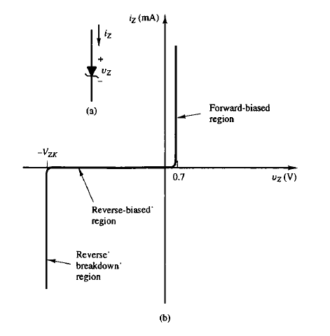
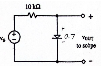
Turn-On Voltage (Vf)
The voltage at which the exponential term begins to dominate the diode current. The v-i characteristic changes from horizontal to vertical. 0.7 V is the standard value, although the range is usually between 0.5 - 0.8 V.
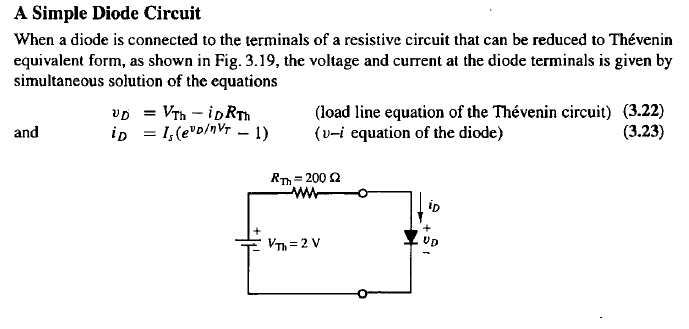
How to Solve a Simple Diode Circuit for VD and iD
Find the intersection of the load line and the v-i characteristic of the diode.
Zener Diode and VZK
In a Zener diode, the current can flow in both directions. It works like a pn-diode in the forward biased region. It has no current in the reverse-biased region. If the voltage in the negative direction is greater than VZK, current will flow.
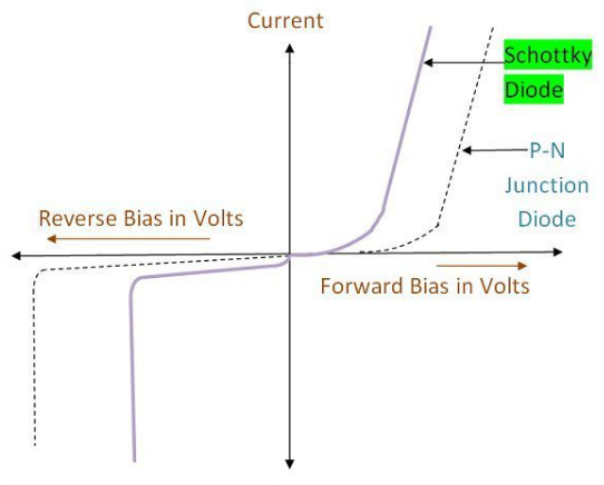
Schottky Diode
A Schottky Diode is known for its low turn-on voltage, which is around 0.3 V compared to 0.7 V. It can switch between reverse and forward bias quicker than most diodes.
Clipping Circuit
A clipping circuit limits, or clips, part of an input signal above or below a certain voltage using diodes. It alters the waveform by removing portions that exceed certain levels.