Comprehensive Nanomaterials & Nanotechnology
1/136
Earn XP
Description and Tags
A comprehensive set of flashcards covering vocabulary and key concepts in nanomaterials and nanotechnology.
Name | Mastery | Learn | Test | Matching | Spaced | Call with Kai |
|---|
No analytics yet
Send a link to your students to track their progress
137 Terms
Superparamagnetism
A magnetic state in single-domain ferromagnetic or ferrimagnetic nanoparticles where thermal energy is sufficient to randomly flip the particle’s magnetization direction.
kbT >= KV
kb = Boltzmann constant (J * K^-1)
T = temperature (K)
K = magnetic ansiotopy constant (J * m^-3)
V = particle volume (m³)
Typical materials
Fe₃O₄ (magnetite)
γ-Fe₂O₃ (maghemite)
Co, Ni nanoparticles
Blocking Temperature (T_B)
The temperature below which a nanoparticle’s magnetization appears “frozen” over the measurement timescale.
Tb = (KV) / (kb ln (τm/τ0)
where:
Tb = Blocking temperature (k)
K = Magnetic Ansiotropy constant (j*m³)
V = Particle volume (m³)
kb = Boltzmann constant
τm = Measurement time
τ0 = Attempt time (~10^-9 seconds)
Blocking temperature is NOT a fixed material constant.
It depends on particle size AND measurement time.
Critical Single-Domain Size
The maximum particle size at which a ferromagnetic particle remains a single magnetic domain.
Domain wall energy vs. magnetostatic energy
Below this size, forming a domain wall costs too much energy
Critical Diameter (D_c)
It determines the size at which a ferromagnetic material becomes a single magnetic domain. Given by scaling arguments involving exchange stiffness (A), anisotropy (K), and saturation magnetization (Mₛ)
Ferromagnetism to Superparamagnetism Transition
A transition characterized by a size-dependent change from multi-domain ferromagnetism to superparamagnetism.
multidomain → single-domain ferromagnet → superparamagnet
Energy Barrier (E_barrier)
The energy required to reverse the magnetization direction of a nanoparticle.
Ebarrier = KV
E = Energy barrier for magnetization reversal (J)
K = Magnetic Ansiotropy constant (J*m^-3)
V = particle volume (m³)
Larger particles → higher energy barrier
Smaller particles → easier thermal flipping
Curie Temperature (T_C)
The critical temperature above which a ferromagnetic material becomes paramagnetic.
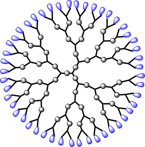
Dendrimers
Highly branched, monodisperse macromolecules with a tree-like structure that encapsulate molecules.
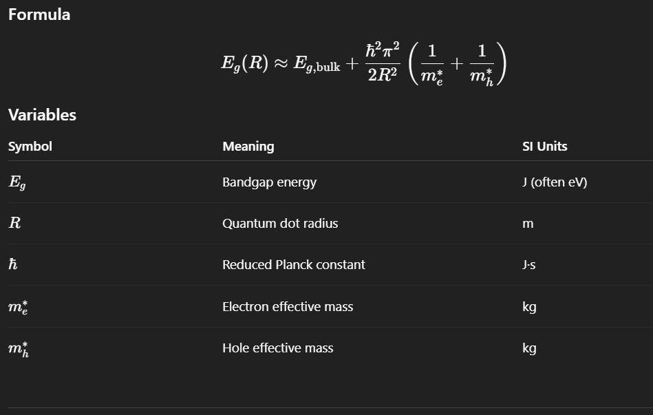
Quantum Confinement
The phenomenon where the electronic and optical properties of materials change as their size approaches the exciton Bohr radius
Confinement occurs when particle size ≲ exciton Bohr radius.
Size-dependent bandgap
Blue shift in optical absorption
Discrete density of states
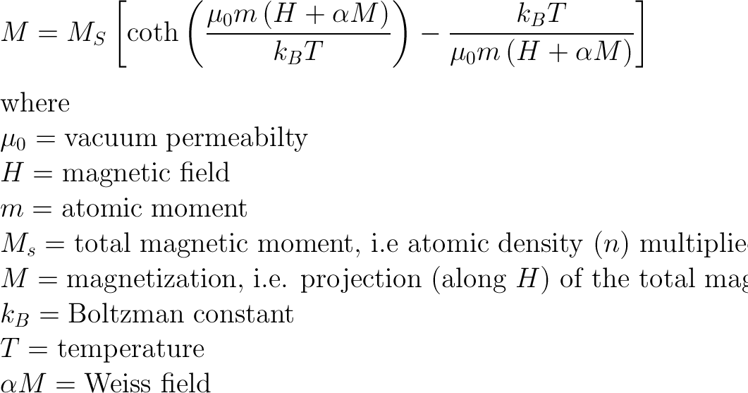
Langevin Magnetization
Shows that magnetization isn't perfectly linear with the field
At low fields/high temps, it follows Curie's Law (proportional to H/T)
At high fields/low temps, the dipoles fully align (saturate), and the function "bends over," balancing alignment forces (field) with randomizing forces (temperature)
Self-Assembly
A process by which components spontaneously organize into ordered structures through non-covalent interactions.
Types
Molecular Self-Assembly – e.g., lipids → bilayers, micelles.
Colloidal Self-Assembly – nanoparticles → crystals or clusters.
Supramolecular Self-Assembly – proteins, DNA structures.
Template-Assisted Self-Assembly – guided by pre-patterned surfaces.
Hydrodynamic Diameter (d_h)
The effective diameter of a particle in a fluid, including the particle itself plus the layer of solvent molecules that move with it. It represents how a particle “appears” when diffusing or moving through a liquid.
Measured through Dynamic Light Scattering (DLS). Use Stokes-Einstein Equation
Scanning Electron Microscopy (SEM)
Provides topography, composition, and sometimes crystallography of a sample.
Samples usually need to be conductive or coated with a thin conductive layer.
Used for:
Metals (Au, Cu, Al) – surface microstructure
Polymers – morphology of fibers or films
Nanoparticles – size and aggregation
Electron Beam:
A focused beam of high-energy electrons scans across the sample surface.
Interactions:
Electrons interact with the atoms in the sample and generate signals:
Secondary electrons → give surface topography (main imaging mode).
Backscattered electrons → reveal composition contrast (heavier atoms appear brighter).
X-rays → give elemental composition (via EDS/EDX detector).
Detection & Imaging:
Detectors collect these signals to form a high-resolution image of the surface.
Resolution can reach ~1–10 nm, depending on instrument and sample.
Transmission Electron Microscopy (TEM)
TEM is a technique that images the internal structure of thin samples at atomic or nanometer resolution using electrons transmitted through the material.
Sample must be ultra-thin for electrons to transmit.
Materials
Metals (dislocations, edge boundaries)
Nanoparticles (shape, size, and crystal structure)
Electron Beam:
A high-energy electron beam passes through a very thin sample (<100 nm thick).
Interactions:
Electrons are scattered by atoms in the sample.
The pattern of transmitted and scattered electrons forms an image.
Can also produce electron diffraction patterns to study crystal structure.
Detection & Imaging:
Fluorescent screen, CCD camera, or detectors collect transmitted electrons.
Images reveal internal structure, not just surface like SEM.
Resolution can reach ~0.1–0.2 nm, allowing observation of individual atoms.
Dynamic Light Scattering (DLS)
DLS is a technique to measure the size (hydrodynamic diameter) and distribution of small particles or molecules in a liquid by analyzing their Brownian motion.
Non-destructive and commonly used for nanoparticles, proteins, and polymers.
How It Works:
Laser Illumination:
A laser beam passes through a colloidal solution of particles.
Scattering:
Particles scatter light in all directions.
Because particles are moving due to Brownian motion, the intensity of scattered light fluctuates over time.
Analysis:
Fluctuations are analyzed with an autocorrelation function to determine the diffusion coefficient DDD of the particles.
Using the Stokes–Einstein equation, the hydrodynamic diameter is calculated:
Scanning Tunneling Microscopy (STM)
Images surfaces at the atomic scale by measuring the quantum tunneling current between a sharp tip and the conductive sample.
Provides atomic-resolution surface topography and can also probe electronic properties.
How It Works / Measurement Principle:
Sharp Tip & Conductive Sample:
A very sharp metallic tip is brought extremely close (~0.5–1 nm) to the sample surface.
Quantum Tunneling:
When a voltage is applied, electrons tunnel through the vacuum between tip and sample.
The tunneling current III depends exponentially on the distance ddd:
I∝Ve-2κd
Where:
V = applied voltage
d = tip–sample distance
κ = decay constant depending on work function
Imaging:
The tip scans across the surface in a raster pattern.
A feedback loop keeps the tunneling current constant by adjusting the tip height.
The tip movement is mapped to create a high-resolution surface image at atomic scale.
X-ray Photoelectron Spectroscopy (XPS)
XPS is a technique to analyze the elemental composition and chemical states of a material’s surface (~1–10 nm) by measuring kinetic energy of electrons ejected by X-rays.
Surface-sensitive and widely used for metals, semiconductors, polymers, and coatings.
How It Works / Measurement Principle:
X-ray Irradiation:
The sample surface is irradiated with monoenergetic X-rays (commonly Al Kα: 1486.6 eV).
Photoelectron Emission (Photoelectric Effect):
X-ray photons eject core electrons from atoms.
The kinetic energy (KE) of the emitted electron is measured.
Binding Energy Calculation:
The binding energy (BE) of electrons is calculated using:
BE = hv - KE - ϕ
Where:
BE= binding energy (electronvolts, eV)
hν= photon energy (eV)
KE = kinetic energy of emitted electron (eV)
ϕ = work function of spectrometer (eV)
Interpretation:
Each element has characteristic binding energies → identify elements.
Small shifts in BE indicate chemical states / oxidation states.
X-ray Diffraction (XRD)
XRD is a technique to analyze the crystal structure, phase, and lattice spacing of materials by measuring the pattern of X-rays diffracted from the atomic planes.
Widely used for metals, ceramics, semiconductors, and nanomaterials.
How It Works / Measurement Principle:
X-ray Irradiation:
A beam of X-rays (typically Cu Kα, λ ≈ 1.54 Å) is directed at the crystalline sample.
Diffraction:
X-rays are scattered by the electron clouds of atoms in the crystal.
Constructive interference occurs when Bragg’s law is satisfied: 2λ = 2dsinθ
Detection & Analysis:
A detector measures the intensity of diffracted X-rays as a function of
The pattern of peaks is used to determine:
Crystal structure (cubic, tetragonal, etc.)
Crystallite size (via Scherrer equation)
Hall-Petch Relationship
Describes how a material’s strength (yield stress) increases as its crystal grain size decreases. Breaks down at very small grain sizes (inverse Hall–Petch)
σy=σ0+kd^(-1/2)
σy = (Yield Strength): The stress at which the material begins to deform permanently
σ0 = The baseline stress needed to move dislocations, independent of grain size, reflecting lattice resistance.
d = grain diameter
k = hall petch constant
Zirconium Oxide (ZrO₂)
A wide bandgap semiconductor known for its thermal stability and applications in optical coatings.
Plasmonic Nanostructures
Structures that exploit localized surface plasmon resonance for applications in sensing and photothermal therapy.
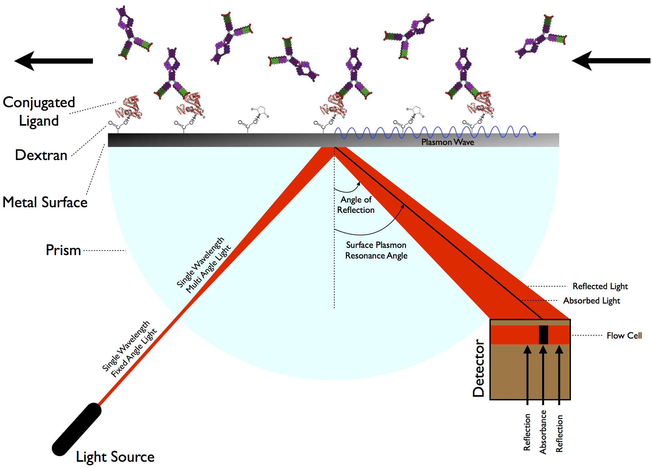
Localized Surface Plasmon Resonance (LSPR)
Collective oscillation of conduction electrons in metal nanoparticles, enhancing light interaction.
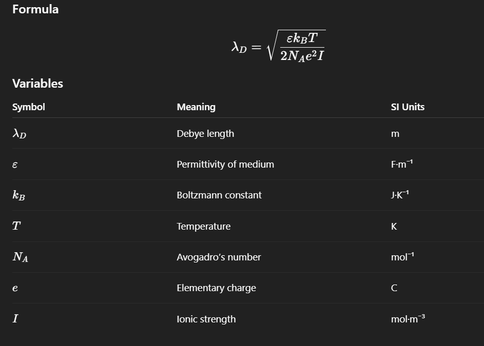
Debye Length (λ_D)
The characteristic length over which electric fields are screened by mobile charges in an electrolyte.
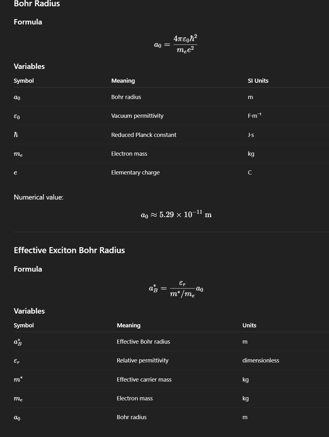
Bohr Radius (a₀)
The scale of the electron wavefunction in hydrogen, approximately 0.529 Å.
Nanoparticle
A three-dimensional confined structure with all dimensions on the nanoscale (< 100 nm).
Nanocrystal
A crystalline nanoparticle that has a well-defined crystal lattice and is characterized by techniques like XRD.
Quantum Dot (QD)
A 0D semiconductor nanocrystal with confinement in all three dimensions.
Materials
CdSe, CdS, PbS
InP (biocompatible alternative)
Nanotubes
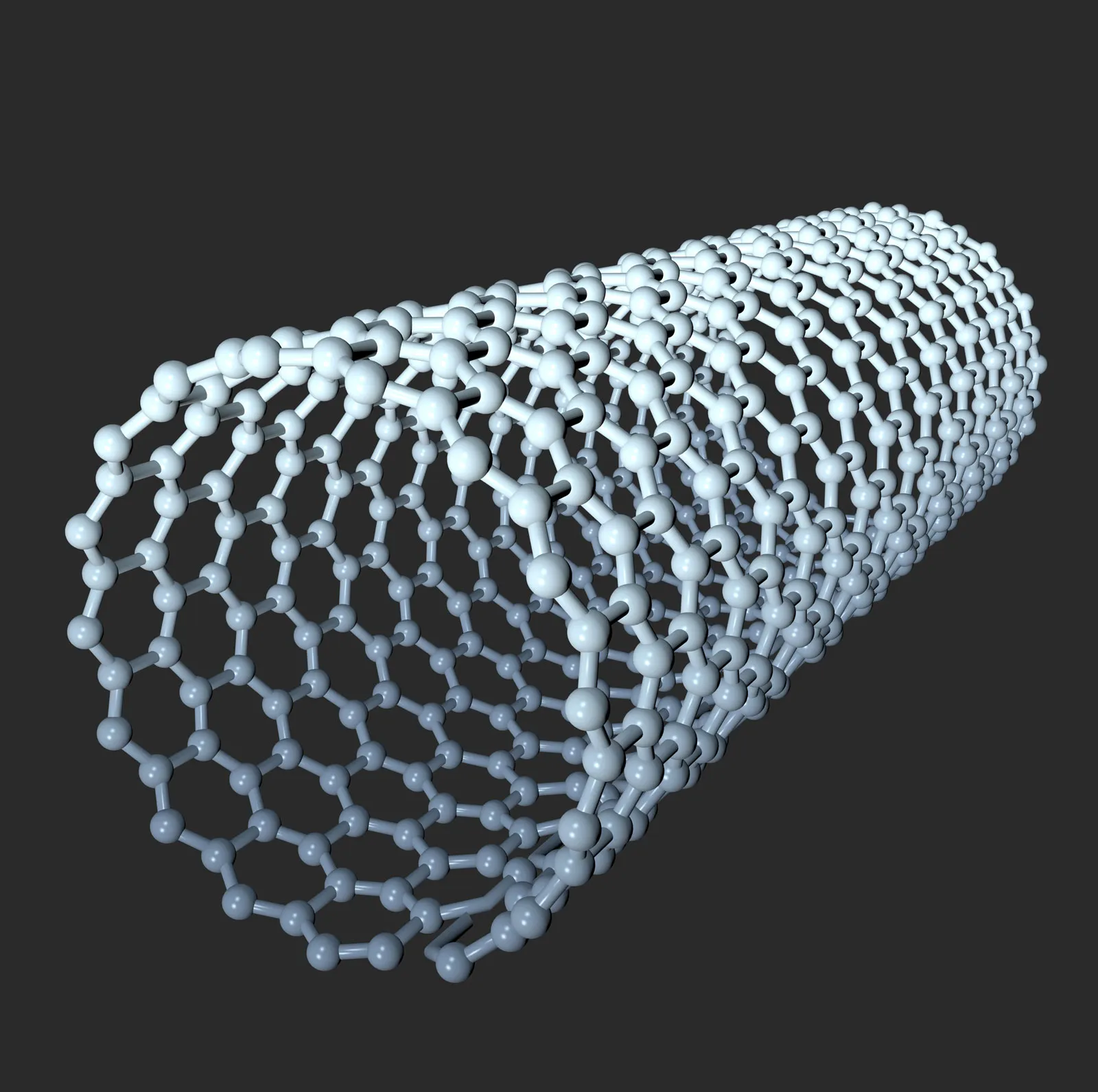
Cylindrical structures of nanomaterials, particularly carbon-based, which exhibit unique electrical properties.
Nanotubes are usually made of rolled-up sheets of atoms:
Carbon Nanotubes (CNTs):
Formed from graphene sheets rolled into cylinders.
Can be Single-Walled (SWCNT) or Multi-Walled (MWCNT).
Properties arise from structure:
Electrical: Metallic or semiconducting depending on chirality (rolling angle).
Mechanical: Extremely strong and stiff due to sp² carbon bonds.
Thermal: Excellent thermal conductivity along the tube axis.
Atomic Layer Deposition (ALD)
Sequential Exposure:
The substrate is alternately exposed to two or more precursor gases.
Each precursor reacts chemically with the surface in a self-limiting reaction, depositing one monolayer per cycle.
Self-Limiting Reactions:
Only available reactive sites on the surface participate → prevents overgrowth.
Cycle Repetition:
Repeating cycles increases film thickness linearly:
3. Relevant Materials / Examples:
Oxides: Al₂O₃, TiO₂, HfO₂
Nitrides: TiN, AlN
Metals: Pt, Ru
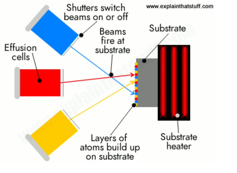
Molecular Beam Epitaxy (MBE)
A method for growing thin crystals by using molecular beams of high purity.
Ultra-High Vacuum Chamber:
Reduces contamination and allows long mean free path for atoms.
Molecular Beams:
Pure elemental sources (like Ga, Al, As) are heated to evaporate atoms.
Atoms travel as molecular beams toward the substrate.
Epitaxial Growth:
Atoms adsorb on the substrate surface, diffuse, and arrange themselves according to the crystal lattice of the substrate.
Layer-by-layer growth enables atomic-scale control of thickness and composition.
Monitoring:
Reflection High-Energy Electron Diffraction (RHEED) is often used in-situ to monitor surface structure and growth rate.
3. Key Materials / Examples:
Semiconductors: GaAs, AlGaAs, InP, SiGe
Heterostructures: Quantum wells, superlattices
Oxides and metals can also be grown with modified MBE systems
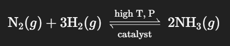
Haber-Bosch Process
An industrial method for synthesizing ammonia from nitrogen and hydrogen gases.
Epitaxial Growth
The deposition of a crystalline overlayer on a crystalline substrate maintaining the orientation of the substrate.
Key Materials / Examples:
Semiconductors: GaAs on GaAs, Si on Si
Heterostructures: GaAs/AlGaAs, InGaAs/GaAs
Oxides: SrTiO₃ on perovskite substrates
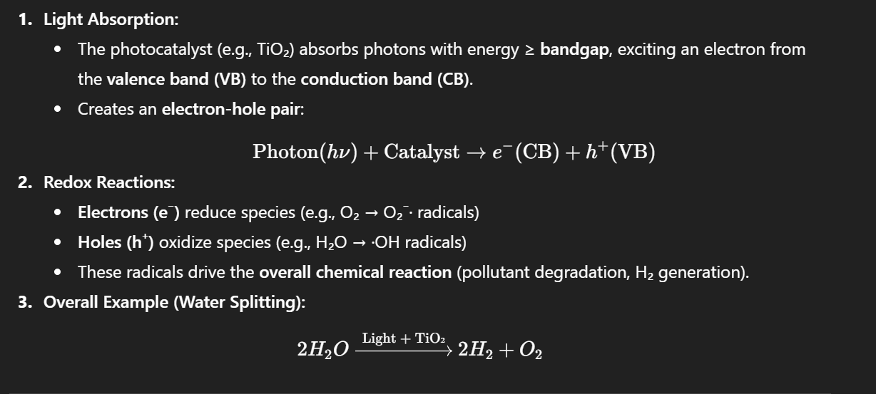
Photocatalysis
A process that uses light to accelerate a photoreaction in the presence of a catalyst.
Relevant Materials / Examples:
Semiconductors: TiO₂ (most common), ZnO, CdS
Doped materials: N-doped TiO₂ (visible light activity)
Nanomaterial
Any material with at least one dimension on the nanoscale, typically defined as ranging from 1 to 100 nm.
Polymer Nanocomposite
Polymer nanocomposites are polymers reinforced with nanoscale fillers to enhance mechanical, thermal, electrical, or barrier properties beyond conventional composites.
Relevant Materials / Examples:
Carbon-based: Carbon nanotubes (CNTs), graphene, carbon black
Clay-based: Montmorillonite (MMT) nanosheets
Metal oxides: TiO₂, SiO₂, ZnO nanoparticles
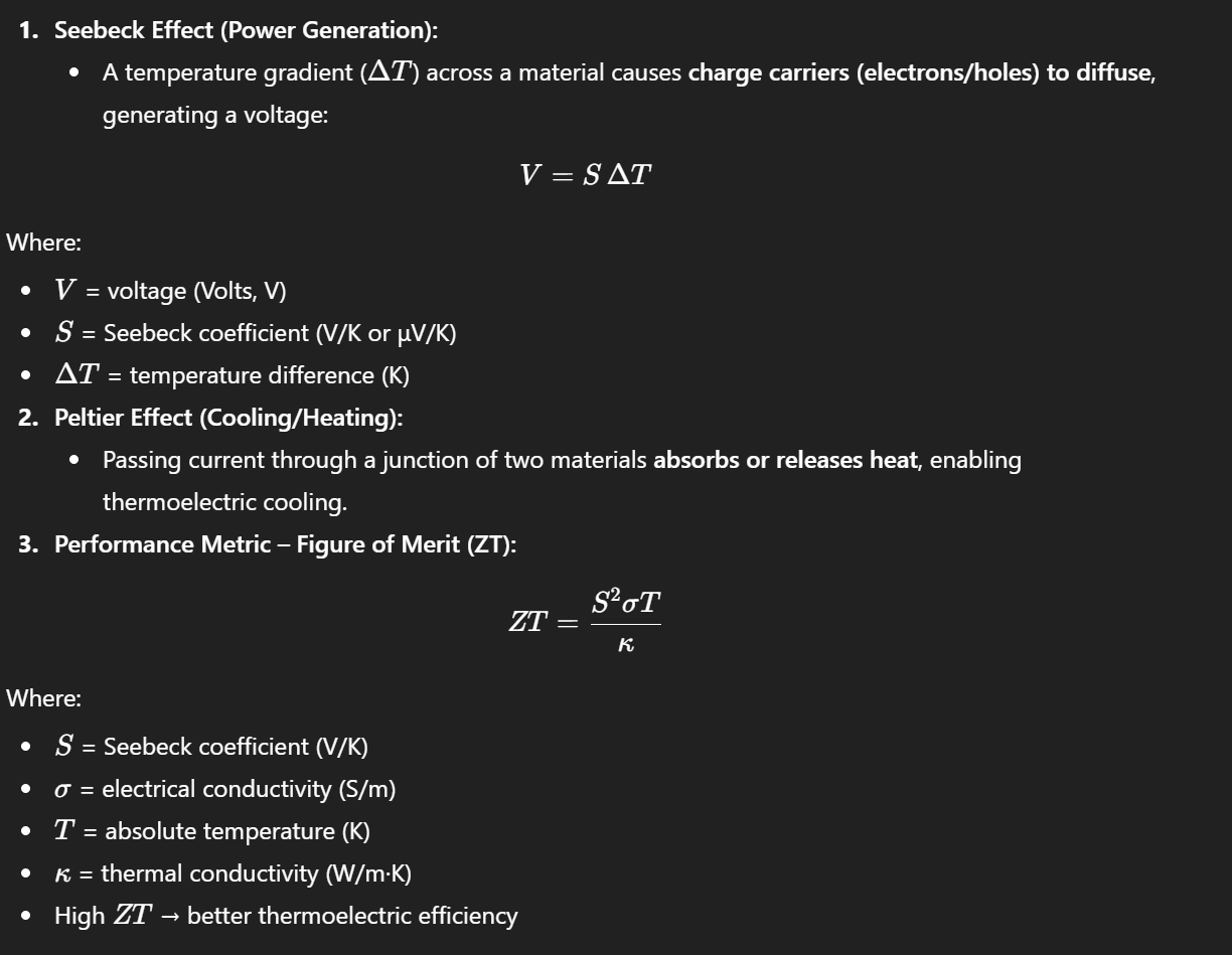
Thermoelectric Materials
Thermoelectric materials convert temperature differences directly into electrical voltage (Seebeck effect) or vice versa (Peltier effect).
Efficiency depends on the material’s electrical conductivity, thermal conductivity, and Seebeck coefficient.
Key Materials / Examples:
Bismuth telluride (Bi₂Te₃) – room-temperature applications
Lead telluride (PbTe) – high-temperature power generation
Silicon-germanium (SiGe) – space thermoelectrics
Skutterudites, Half-Heusler alloys – advanced thermoelectric materials
Acoustic Imaging
A form of imaging; can use nanoscale contrast agents, but spatial resolution is typically microscale
Sound Wave Generation:
A transducer emits high-frequency sound waves (typically 1–15 MHz for medical imaging).
Wave Propagation & Reflection:
Sound waves travel through the medium and are partially reflected at interfaces where acoustic impedance changes:
Z=ρc
Where:
Z = acoustic impedance (kg/m²·s)
ρ = density of the medium (kg/m³)
c = speed of sound in medium (m/s)
Resolution:
Axial resolution: Δz = c/(2f)
Where:
f = frequency of ultrasound (Hz)
c = speed of sound in medium (m/s)
Carbon Nanotubes (CNTs)
Mechanical Properties
Extremely high tensile strength: ~50–200 GPa (stronger than steel by weight)
High Young’s modulus: ~1 TPa (stiff, very resistant to stretching)
Lightweight: density ~1.3–1.4 g/cm³ (much lighter than metals)
Flexibility: can bend without breaking and recover shape
Electrical Properties
Metallic or semiconducting depending on chirality (n,m)(n, m)(n,m)
High electrical conductivity: up to 10⁶–10⁷ S/m for metallic CNTs
Thermal Properties
High thermal conductivity: up to 3000–3500 W/m·K along the tube axis (better than copper)
Good thermal stability: can withstand >600 °C in air, ~2800 °C in vacuum
Chemical Properties
Chemically stable due to sp² carbon bonding
Can be functionalized to attach chemical groups → improves solubility or adds new functionality
Optical Properties
CNTs can absorb light in UV–NIR range
Exhibit photoluminescence in semiconducting CNTs → useful for bioimaging and sensors
Metal Oxide Nanoparticles
Nanoparticles formed from metal oxides, which exhibit unique electrical properties and stability.
Relevant Materials / Examples:
TiO₂: photocatalysis, sunscreens, self-cleaning surfaces
ZnO: UV-blocking, antibacterial, electronics
Fe₃O₄ / Fe₂O₃: magnetic nanoparticles for MRI, drug delivery
CeO₂: redox catalyst, antioxidant in biomedical applications
CuO, Co₃O₄, NiO: catalysis, sensors, energy storage
Nanowires
Structure:
Diameter: 1–100 nm
Length: up to several microns → very high aspect ratio (length/diameter)
Quantum Effects:
Electron motion is confined in the transverse direction → quantum confinement
Leads to size-dependent optical and electronic properties
Conductivity and Carrier Transport:
High surface-to-volume ratio → surface scattering affects electron mobility
Can exhibit ballistic transport over short distances
Relevant Materials / Examples:
Semiconductors: Si, GaAs, InP
Metals: Au, Ag, Cu
Oxides: ZnO, TiO₂
Nanofilms
Thin films of nanostructured materials, often used for coatings.
Electron motion is restricted perpendicular to the film → quantum confinement
High surface area → surface interactions dominate properties
Relevant Materials / Examples:
Metals: Au, Ag, Pt → plasmonics, electrodes
Semiconductors: Si, GaAs → electronic devices
Oxides: TiO₂, ZnO → photocatalysis, sensors
Plasmonic Sensors
Plasmonic sensors use surface plasmon resonance on metallic nanostructures to detect tiny changes in refractive index near the surface.
Quantum Wells
A quantum well is a thin layer of a low-bandgap semiconductor sandwiched between higher-bandgap semiconductors, creating confinement of charge carriers (electrons and holes) in one dimension.
Semiconductors: GaAs/AlGaAs, InGaAs/InP
Quantum Wires
Nanostructures confined in two dimensions, allowing charge carriers to move freely in one dimension.
Quantum Dots
Quantum dots are zero-dimensional semiconductor nanostructures where electrons and holes are confined in all three spatial dimensions, leading to discrete, atom-like energy levels.
When nanoparticles get to a certain size, shit starts to hit the fan and nothing works the same
This usually occurs at ~2-10nm or 10-15 atoms. Some are the size of molecules.
Quantum mechanical effects (confinement) messes everything up
Small QDs are blue and larger ones are red
When illuminated by a certain wavelength, QDs electrons can be excited
Commonly used in displays
Used in solar cells to capture a broader spectrum of light
Called tunable photoluminescence
Used in biology as a dye
Thermal Conductivity
A measure of a material's ability to conduct heat.
k = (1/3) Cvl
C = heat capacity
v = phonon velocity
l = mean free path
Phonon Mean Free Path
Average distance a phonon travels before scattering.
l = vτ
l = Mean free path (m)
v = phonon velocity
τ = Relaxation time
Zirconium dioxide
A widely used ceramic material known for its hardness and thermal stability.
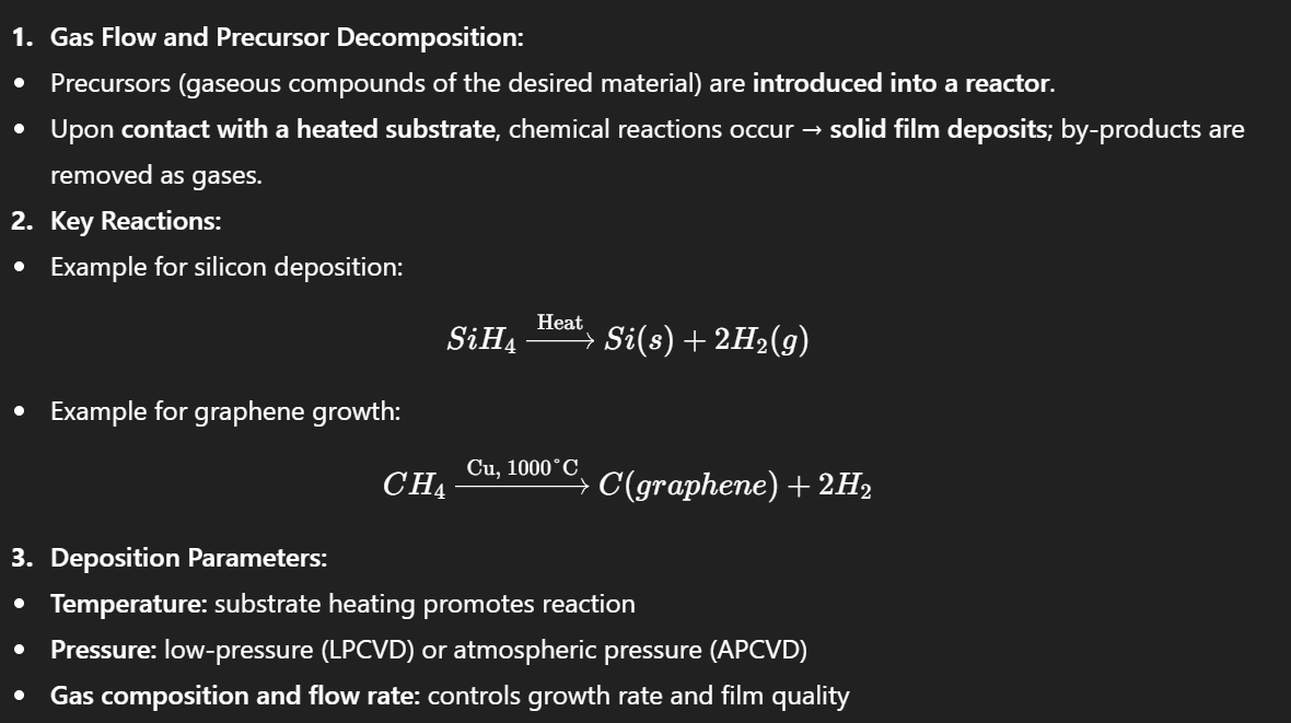
Chemical Vapor Deposition (CVD)
Chemical vapor deposition (CVD) - involves using gaseous precursors that react of decompose onto a substrate, creating the desire material.
Usually done by filling a heated chamber with chemical precursors that react and fall onto the substrate.
Often creates volatile by-products which are removed by a gas flow/purging process
Commonly used to make thin films
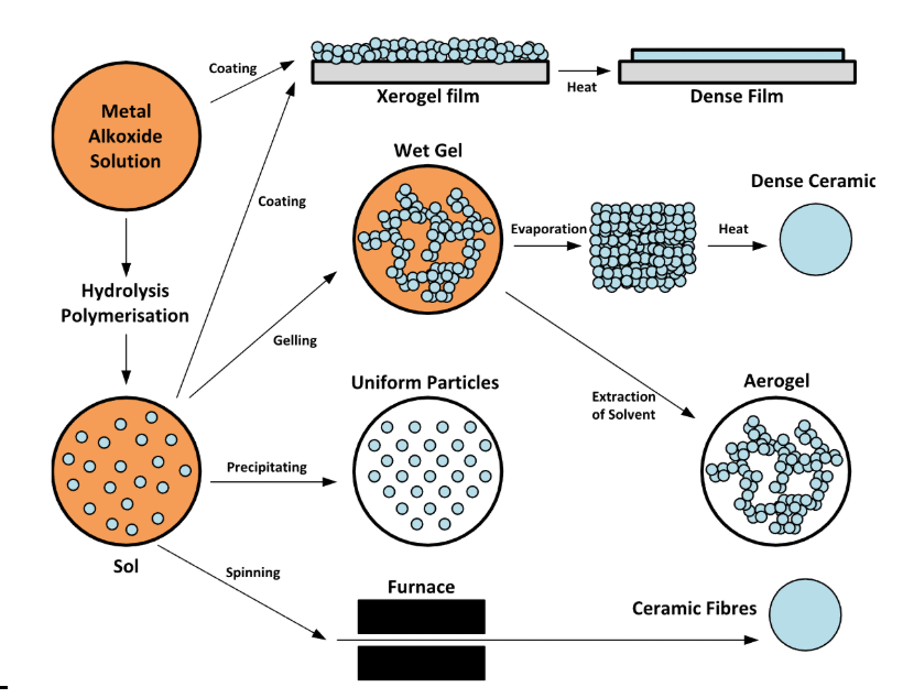
Sol-Gel Process
A method for producing solid materials from small molecules, usually involving the transition from a liquid solution to a solid gel.
Nanostructured Supercapacitors
Nanostructured supercapacitors are high-surface-area energy storage devices that store charge via double-layer formation or pseudocapacitive redox reactions, offering fast charge/discharge and high power density.
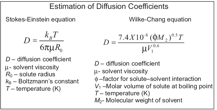
Stokes-Einstein and Wilke-Chang
Stokes-Einstein: Used for nanoparticles like Au
Wilke-Chang - Small molecules (solutes) like Ethanol
Van der Waals
Weak electric forces
Weak bonds
Strongest:
Repulsive force from Pauli Exclusion Principle
Keesome Force
Repulsive/attractive force between permanent charges
Debye Force (Induction, polarizability)
Permanent pole and an induced pole
London Dispersion Force
Temporary Instantaneous induced poles on each other.
Semiconductors
N-type
Electrons are the charge carriers
P-type
Holes are the charge carriers
Metallic Ionic
Metal donates electron density to a more electronegative element.
Some electrons remain in partially filled bands → metallic conductivity.
Covalent Ionic
Electron density is shared but shifted toward the more electronegative atom.
Produces polar covalent bonds.
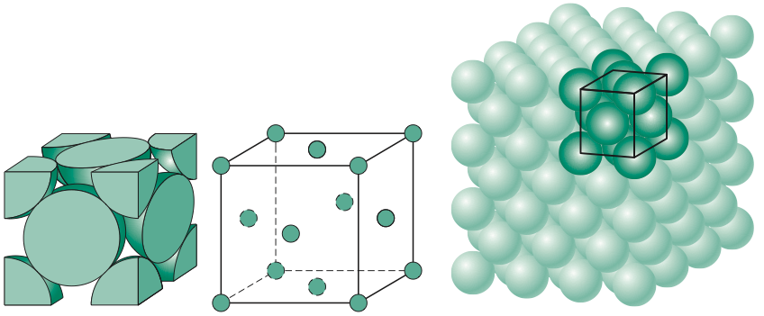
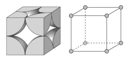
Face Centered Cubic / cubic packed
ABCABC close packing pattern
Atomic packing factor of .74
Unit cell has 4 atoms
Side length = 4Rsqrt2
Coordination number = 12
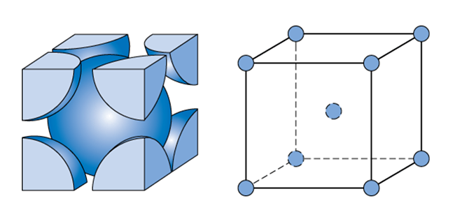
Body centered cubic
Atomic packing factor of .68
Unit cell contains 2 atoms
Side length = 4Rsqrt3
Coordination number of 8
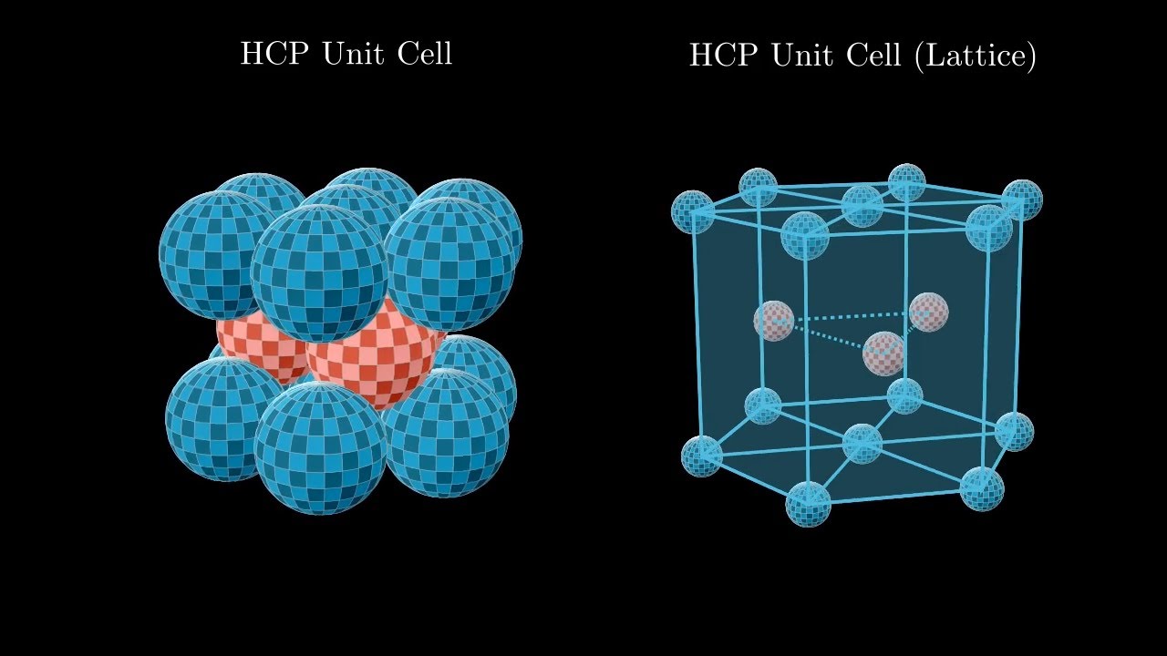
Hexagonal Close packing
ABAB packing pattern - 2 repeating layers
Atomic packing factor of .74
Unit cell has 6 atoms
Coordination number of 12
Simple Cubic
Atomic packing factor of .52
Unit cell has 1 atom
Side length = 2R
Coordination = 6
Atomic Packing factor
How efficiently atoms are packed within a unit cell
APF = (volume of atoms in a unit cell) / (total unit cell volume)
Coordination number
Number of nearest-neighbor atoms around a given atom
Point Defects
Localized disruptions in a crystal lattice involving only 1 or 2 atomic positions.
Linear Defects
One-dimensional (1-D) disruptions in the regular arrangement of atoms within a crystal.
Interfacial Defects
Two-dimensional (2-D) boundaries, such as grain boundaries or surfaces, that separate regions of different crystallographic orientations or structures.
Stoichiometric vs. Non-Stoichiometric Defects
Stoichiometric Defects: Do not change the overall ratio of cations to anions in the compound.
Non-Stoichiometric Defects: Result in a change in the ratio of cations to anions.
Vacancies
A point defect characterized by an atom missing from its normal lattice site.
Can be caused by thermal vibrations or non-stoichiometric conditions.
Interstitial Cations
Cations that occupy normally unoccupied interstitial sites in the lattice, causing local distortions.
Impurities
Foreign atoms within a crystal that either substitute for host atoms (substitutional) or occupy interstitial sites (interstitial).
Frenkel Defect
A point defect in ionic solids where a cation leaves its normal lattice position and occupies a nearby interstitial site.
Schottky Defect
A point defect in ionic solids where an equal number of cations and anions are missing from the lattice, maintaining charge neutrality.
Edge Dislocation
A linear defect caused by an extra half-plane of atoms inserted into the crystal structure.
Screw Dislocation
A linear defect where the lattice atoms are displaced in a spiral or helical pattern around the dislocation line.
Grain Boundaries
The interface where two grains of different crystallographic orientations meet within a polycrystalline ceramic or metal.
Twin Boundaries
A specific type of interfacial defect where there is a mirror symmetry in the arrangement of atoms across the boundary.
Porostiy
Void spaces within a material, percentage of total volume
Higher porosity, higher absorption
Porosity (%) = (Volume of Voids / Total Volume) x 100
Open porosity
Pores are interconnected and accessible to the surface
Higher absorption
Higher permeability
Closed pores
Isolated pores that are not connected to the surface
Lower absorption
Lower permeability
Unary phase change
Single compound vs temperature or pressure
Binary phase change
You have a material composed of elements A and B. Y axis is temperature or pressure, and X axis is the percent of element B in the compound
Engineering stress and strain
σ = F/A
ε = ΔL / L0
Used when area barely changes
True stress and strain
σ = F/A
ε = ln(L / L0)
Relationship between engineering and true stress/strain
Used during uniform deformation
σtrue = σeng(1+εeng)
εtrue = ln(1+εeng)
Ductility
(A0-Af)/A0 * 100%
Stress σ vs Strain graph ε

Elastic region
Follows Hooke’s Law σ = Eε
Young’s (Elastic) Modulus is slope: E= σ/ε
Yield Strength
Plastic deformation
Dislocations happen in bulk
Atomic planes slip past each other
Upper yield strength
Caused by a temporary build-up of resistance to plastic deformation from interstitial atoms (like carbon and nitrogen) that lock dislocations within the material
Afterwards they slide past each other
Lower Yield strength
Once the dislocations are free, the applied stress needed to keep them moving is significantly lower.
Plastic region
σ = Kεn
K is strength coefficient
n is strain-hardening component (0-1) for most metals)
Strain hardening
Continued plastic deformation creates many more dislocations.
These dislocations interact, tangle, and block each other.
Because motion is harder, the material needs more stress to continue deforming
Necking
Reaches ultimate tensile strength
Maximum engineering stress
Local region becomes thinner than the rest and experiences a higher stress
Considère criterion
(dσtrue)/(dεtrue) = σtrue
Flexural Strength
Strength under bending
3 point bending σf = (3FL)/(2bd^2)
4 point bending σf = (FL)/(bd^2)
F = load at fracture, L = support span, d = specimen length, d = specimen thickness
Compressive Strength
Maximum stress before failing in compression
σ = Fmax / A
Fracture Toughness (K_IC)
How well a material can handle cracks
KIC = Yσ sqrt(πa)
a is crack length
Y is geometry factor
Brittle Fracture
If a crack of length a already exists, how much tensile stress will break the material? Applies to brittle materials ONLY.
σc = sqrt((2Eγ)/πa)
Bragg’s Law
nλ = 2d sin θ
n: diffraction order (integer, dimensionless)
λ: wavelength of incident radiation (length, meters or Å)
d: distance between crystal planes (meters or Å)
θ: Bragg angle (degrees or radians)
Thermal Expansion
ΔL = a L0 ΔT
Higher a means more expansion per degree
Thermal Conductivity
q = -k(dT/dx)
Rate at which heat flows through material
q: heat flux (W/m^2)
k: thermal conductivity (W/(m*k))
dT/dx: temperature gradient
Larger k is a good conductor
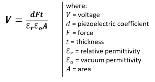
Piezoelectricity
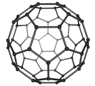
Fullernes
Resembles a hollow cage-like structure. Can take a spherical, ellipsoid, or tube-like shapes
Denoted by Cn where n indicates the number of carbon molecules
The most famous fullerene, buckminsterfullerene is denoted by C60 and can be found naturally. Image of buckminsterfullerene below.
Fullerenes with less than 60 carbon atoms are called ‘lower fullerenes’ and those with greater than 70 are called ‘upper fullerenes’
Applications include MRI & X-ray contrasting agents, drug & gene delivery, and tumor treatment
Graphene
Visible to the naked eye, graphene is 2D nanomaterial at the atomic scale. It is a sheet of carbon molecules.
Carbon atoms interlock in hexagons to form a honeycomb like structure
Multiple layers of graphene is called graphite
First discovered by scientists who used scotch tape to lift an atom thick layer off of a graphite block
Strongest material at the microscopic scale
Applications include as a lubricant (in powdered form), as a protective coating, in electronics, and in biosensors