Chemistry and Materials Science Final Exam
1/84
There's no tags or description
Looks like no tags are added yet.
Name | Mastery | Learn | Test | Matching | Spaced | Call with Kai |
|---|
No analytics yet
Send a link to your students to track their progress
85 Terms
FCC
a) structure
b) number of atoms (n)
c) coordination number
d) relationship between atomic radius and lattice parameter (a)
e) along what do atoms touch?
a) 1/8 of an atom in each of 8 corners, ½ atom on each of 6 faces, ABCABCABC…
b) n=4
c) CN=12
d) a=(2√2)r
e) along the face diagonals
BCC
a) structure
b) number of atoms (n)
c) coordination number
d) relationship between atomic radius and lattice parameter (a)
e) along what do atoms touch?
a) 1 atom in centre, 1/8 atom on each vertex
b) n=2
c) CN=8
d) a=(4/√3)r
e) along the cube diagonals
Rock Salt
a) structure
b) number of atoms (n)
c) coordination number
d) relationship between atomic radius and lattice parameter (a)
e) along what do atoms touch?
a) position anions in FCC
cations: ¼ atom on each edge, one atom in the centre
b) 4 anions 4 cations
c) CN=6 (each anion is surrounded by 6 cations and vice versa)
d) a=2R(anion)+2R(cation)
e) along cube edges
NOTE: for simple cubic, they also touch along cube edges. a=2r for simple cubic
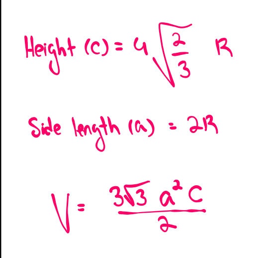
HCP
a) structure
b) number of atoms (n)
c) coordination number
a) ½ atom on the top and ½ on the bottom, 3 atoms inside, 1/6 atom on each of 12 vertices, ABABAB…
b) n=6
c) CN=12
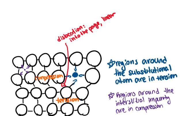
Diamond cubic
a) structure
b) number of atoms (n)
c) coordination number
d) relationship between atomic radius and lattice parameter (a)
a) first draw FCC. Then, add 4 atoms inside, each ¼ of the way along the cube diagonal, so that each atom is bonded tetrahedraly at 109.5 degrees to 4 neighbouring atoms
b) n=8
c) CN=4
d) a=(8/√3)r
nano (ten to the power of…)
-9
micro
-6
milli
-3
mega (M)
6
Giga
9
Tera
12
APF (atomic packing factor)
fraction of volume occupied by spheres
(n*volume of one atom)/(volume of unit cube)
0.74 for FCC and HCP, can’t be higher than that ever
Plastic deformation mechanism (what’s going on)
rows of bonds breaking step by step
step by step movement of linear imperfections
bonds break only a few at a time due to imperfections slowing deformation
what are the 3pt bend test and tensile test used to determine
E (young’s modulus)
Tempered glass
glass heated, then rapidly cooled
surfaces cool faster, compressing as they do. centre is still molten
when core cools, it is in tension since surfaces are in compression
ceramics are stronger in COMPRESSION. The surfaces can resist force, the core balances them out
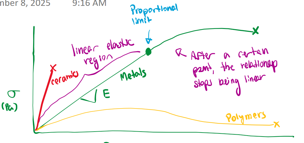
Metal stress strain curve features
Starts at 0. First follows linear relationship with E as slope (linear elastic region)
0.2% yield strength: good estimate for the end of elastic deformation/onset of plastic deformation.
Find strain=0.002
From there, draw a line parallel to linear elastic region
stress at the point where this line intersects the curve is yield stress
after yield strength: uniform plastic deformation
peak of curve: ultimate tensile strength (onset of necking)
necking: non-uniform plastic deformation, curve falls until fracture (cross sectional area decreases rapidly)
necking
starts at UTS. Ends at fracture
Strain hardening of metal does not increase fast enough to keep up with stress increase due to decreased x-sectional area
pico
-12
octahedral interstitial site
When CN=6
imagine cartoon diamond shape
present in FCC, HCP, rock salt
Can fit an atom with radius of 0.414 times the radius of the atoms that make up the lattice
Engineering stress (relate to necking)
F/INITIAL area, so as actual area decreases engineering stress decreases (on the graph)
proportional limit
yield strength
Why don’t ceramics plastically deform?
Metals: layers sliding over one another
Ceramics: cations and anions normally in chess-board pattern, but if you slide them they end up adjacent to like charges and repel
MPI
Material Property Index
On a log(E) vs log(density) graph, we want to maximize MPI (High MPI means high E low density)
Young’s modulus: definition and 3 things that CAN change it
Definition: Measure of how stiff an atom’s bonds are when you ELASTICALLY deform them (not plastic deformation!)
To change it:
Change the bond type/strength
Change atomic spacing
Change polymer crystallinity
Does plastic deformation affect atomic spacing/bond length?
No
Stress relaxation
Occurs in polymers, elastomers, composites:
When stress decreases overtime while held at the same pressure, occurs faster at higher temperatures
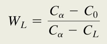
Lever rule (phase diagrams) - what does it tell us?
Ex. we are looking at 5 wt% C at 1000K, and at that point 2 phases are present: A and B
Using tie lines: we can see what percent composition C A is, and what composition C B is. (ex. maybe A is 10 wt% C and B is 40 wt% C)
Using the lever rule, we can find out the actual weight fraction of each phase (ex. 2/10 of the total mass is made up of the A phase)
Lever rule formula
(Weight of your phase / Total weight) = Composition (wt%, using tie line) of the phase you don’t want minus the overall wt% at the point you’re looking at, all over the composition of the phase you don’t want minus composition of the one you do want
How do you find standard combustion enthalpy of a reaction?
Standard formation enthalpy of PRODUCTS minus REACTANTS (P minus R)
Conductor band structure
Conduction band on top, valence band on the bottom
Insulator band structure
Conduction band on top, valence band on bottom, large band gap (for electrons to be conducted an electron would need enough energy to be promoted across the huge band gap)
Note: electrical conductivity CAN occur in an insulator if an electron gets enough energy to cross the band gap. In the conduction band, it is free to move
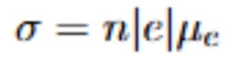
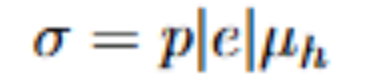
Intrinsic semiconductors and formula for their conductivity
Intrinsic:
one hole created per promoted electron
all charge carriers come from the semiconductor itself
for attached formula: n=p for instrinsic, and q/e (the elementary charge) is always equal, so you can write it as sigma=nq(mn+mp)
sigma: conductivity
n: number of holes=number of electrons
q: fundamental charge
mn/mp: electron and hole mobilities
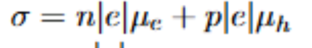
Extrinsic semiconductors
Added impurities (dopants) to control conductivity
2 ways to dope:
n-type (adding electrons)
add anything with MORE valence electrons than your semiconductor (RIGHT on periodic table)
p-type (adding holes)
add anything with FEWER valence electrons (left on periodic table)
n-type semiconductor band structure
valence band at the bottom, then smaller band gap, then conduction band.
small line BELOW conduction band (right at the top of the band gap) is the DONOR level
adding a dopant with extra electrons: the new electron is weakly bonded, easily promoted, very little energy to promote
“donor energy level”: contains the added electrons that are easy to promote
What type of defect are the dopant atoms in extrinsic semiconductors
point defects
p-type semiconductors band structure
Same as n-type, except small “acceptor level” at the bottom of the band gap, just above the valence band
Doping elements with fewer valence electrons adds a hole for each dopand atom
electrons can be promoted to holes with much less energy. The holes create the acceptor energy level
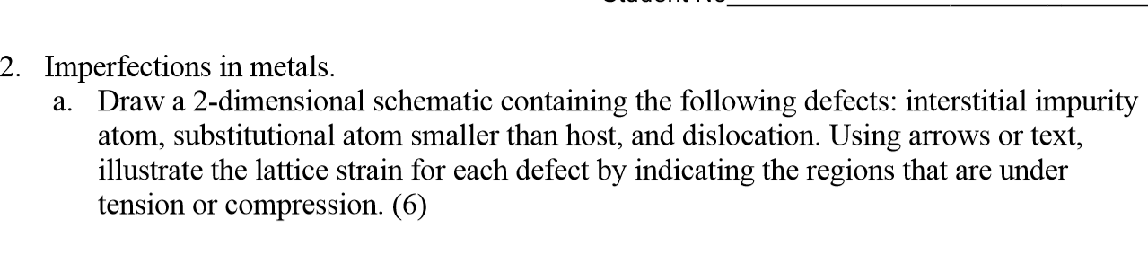
Point defects (and 3 examples)
If the defect concerns one specific atom’s position, composition, or site occupancy, it’s a point defect.
ex:
vacancy (missing atom)
interstitial occupancy (extra atom squeezed in)
substitutional impurity (like replacing an Si atom with a dopant atom
Linear imperfections
Defects with length, but very small width
plastic deformation
dislocation movement
edge dislocation
Interfacial defects
2-D: boundaries between two regions with different phases, orientations, or structures (any FLAT region separating two parts of a material)
ex.
grain boundaries
phase boundaries
Volume defects
3-D:
ex.
voids (holes)
cracks
pores
inclusions (like oxide particles in steel)
cluster of vacancies
anything that has a width, height, and length of more than one atom, that would be visible under a regular microscope
How do polymers continue load bearing after necking?
Molecules become oriented along the loading axis
oriented polymers are MUCH stronger
“deformation by drawing” strengthening mechanism: drawing out polymers to orient them
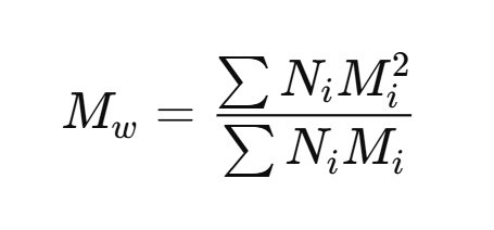
For polymers, what does molecular weight describe
How long they are
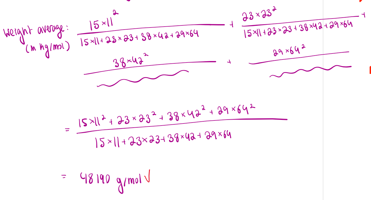
2 ways to describe average molecular weight (length) for polymers
number average
sum of all the weights over the number of molecules (easy)
weight average
Sum of weighted fractions of each “bin” over the total
Weight average: how do you calculate it?
ex. imagine we have a bunch of polymers of different lengths, grouped by their lengths into different “types”
In the attached formula, Mw is weight average, Ni is the number of chains of type i, and Mi is the mass of the chains in that group.
What is the max percent crystalline that a polymer can be? the max percent amorphous?
Can’t be more than 80% crystalline
Can be 100% amorphous
Crystalline vs amorphous polymers strength
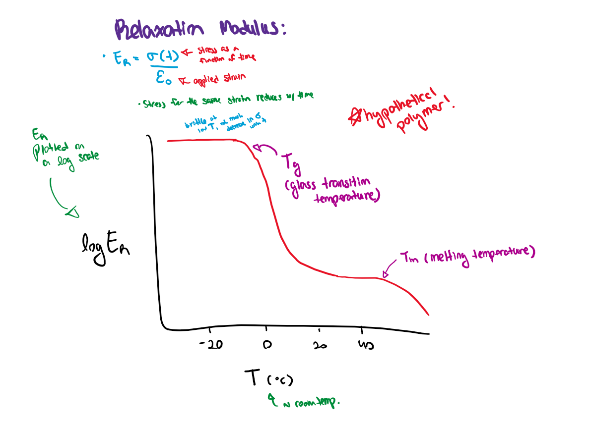
Relaxation modulus
E=(stress as a function of time, sigma of t) / strain
Stress for the same strain reduces with time
Relaxation modulus vs time features
As temperature increases:
Tg - thermal energy overcomes weak secondary interactions in amorphous regions (glass transition temp)
Tm - thermal energy overcomes weak secondary interactions in crystalline regions (melting temp)
Requirements for optical transparency
no internal scattering events
HIGH band gap (why fully amorphous metal’s aren’t transparent - no band gap)
What is an electron volt
1 eV = 1.602 × 10^-19 J = q (the fundamental charge)
What is the faraday constant
The charge of one mole of electrons:
equal to q, or 1 eV (the charge of one electron) times Avagadro’s number (the number of electrons in a mole, or the number of anything in a mole)
what quantum number describes size of orbit? what can it be?
n
n can be 1,2,3,4, etc
what quantum number describes shape? what can it be?
l (always l=n-1)
l=0: s shaped (sphere)
l=1: p shaped (dumbell)
l=2: d
l=3: f
(only s and p orbitals are involved in bonding)
what quantum number controls orientation
ml (must be between -l and l)
ex. for p-subshell, (l=1) this one can be -1, 0, or 1. There are three possible ways to orient a p orbital. For s (a sphere) there is only one
what quantum number controls spin
ms (can only be -1/2 or 1/2)
Slightly different energy level for 2 electrons in the same orbital, so they are distinguished based on their spin. In any given orbital, there can be at most 2 electrons
Cr and Cu electron configurations
Cr: [Ar]3d54s1
Cu: [Ar]3d104s1
Non-directional bonding (def and examples)
All electrons are equally attracted to all neighbours (ex. ionic, metalllic)
Directional bonds
Covalent - only occur between specific atoms
Explain band theory
electron configurations - very distinct energy levels, describing just one atom
But what if we have a solid with a lot of atoms very close to one another?
atoms can’t share energy levels, so as they get very close, their energy levels slightly spread out so for each energy level that you would have in an isolated atom there are 2 when 2 atoms are close by, 3 for 3 atoms, up until you get a huge band that is basically a continuous spectrum
Entropy definition
q(rev)/T (heat transferred reversibly over temperature in K)
delta U (change in internal energy)
(energy change required to make more products) - (energy required to make more reactants)
State function vs path function, one example of each
State - doesn’t matter how we got there (temp, U)
Path - work
Isolated vs closed system
Isolated: No heat exchanged with surroundings, delta U is 0
Closed: heat can pass (no matter exchanged for both)
delta U = q + w
(change in internal energy is equal to heat transferring IN to the system plus work done ON the system)
When is Δ U = q+w
closed system
Positive Δ H?
Endothermic
Equilibrium definition
forward and reverse reactions proceed at the same rate
K vs Q equilibrium
Q - reaction quotient
K - what Q becomes AT EQUILIBRIUM (equilibrium constant)
If the reaction favours the products (forward reaction is spontaneous) what do we know about ΔG plimsol and K
ΔG plimsol is less than zero
K is greater than 1
(vice versa for favouring reactants)
Standard reduction potential: who is more likely to get reduced?
The one with the more positive standard reduction potential
Nernst equation what does it tell us
first equation under electrochem in the data booklet (with the two Es)
lets us find cell potential at concentrations and temperatures that aren’t equilibrium (E plimsol is the equilibrium one)
Range of radius ratios for different interstitial sites and their CN
less than 0.414: tetrahedral (CN 4)
0.414-0.732: octahedral (CN 6)
more than 0.732: cubic (CN 8)
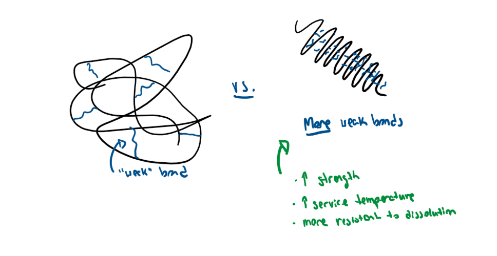
4 polymer strengthening mechanisms
strain hardening - drawing them out along the loading axis, creating friction that resists sliding
cross linking - creating permanent ionic or covalent bonds between chains, resisting sliding and greatly increasing strength (and young’s modulus!)
increasing crystallinity - increased stiffness, density, strength
increasing chain length - more entanglement
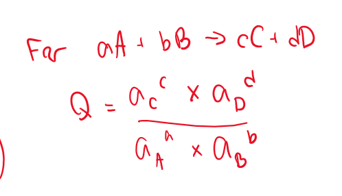
Reaction quotient
Q
a of each species is its activity
concentration
OR
Partial pressure (if it’s a gas)
Usually okay to leave it in terms of partial pressure if not given!
How do you do weight average like for real
multiply how many are in that group by the weight of each thing in that group squared, over the sum of ALL the groups number times weight (a bit confusing but ill attach an example)
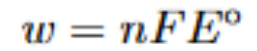
What is this formula
should be w=-nFE
work done by the cell is equal to (negative) number of electrons transfered, times faraday constant, times E of the cell (which is the cell potential, equal to E of the one being reduced minus E of the one being oxidized). This is the same as the gibbs free energy of the cell, delta G equals -nFE
What is this at equilibrium
Reaction gibbs energy is zero at equilibrium and Q is K, so it becomes
Standard G = -RTlnK
What is solid solution strengthening and does it affect Young’s modulus
dissolving atoms of another element into the crystal lattice of a metal, yes it can increase it
what is cold working and can it impact young’s modulus
shaping (rolling, bending, etc) a metal at around room temp to cause work hardening, increasing strength and stiffness but reducing ductility (can affect young’s modulus but not a lot and probably say no for this exam)
How does plastically deforming a metal change its mechanical properties
Plastically deforming it greatly increases the number of dislocations
increased dislocation density makes it harder for dislocations to move
plastic deformation IS the movement of dislocations, so it makes plastic deformation harder
this is what STRAIN HARDENING is
increases yield strength and hardness, NOT stiffness (no change to E)
Describe how you would answer this question
what do you keep forgetting for
a) APF
and
b) entropy
a) you have to multiply by the number of spheres
b) it is given in J, you need to convert
What type of polymers can melt? What type decompose and don’t melt?
Thermoplastics melt
NOT cross linked/network
long, linear chains with weak forces between them
Thermosets don’t met, they char/burn
chain linked/network polymers
strong, permanent
describe how to draw diamond cubic and what’s going on
FCC
the cube has 4 diagonals. following these 4 diagonals, pick 4 vertices (one on each diagonal) so that 2 are on top 2 on the bottom, and 2 are at the front 2 at the back
¼ of the way along the diagonals, there is an atom. It is bonded to 4 other atoms: the one in the corner it is closest to, and the 3 atoms on the 3 faces that that corner is touching
Something doesn’t conduct electricity. Relate that to band theory
insulators have a large band gap