semiconductors
1/53
Earn XP
Description and Tags
final test
Name | Mastery | Learn | Test | Matching | Spaced | Call with Kai |
|---|
No analytics yet
Send a link to your students to track their progress
54 Terms
JFET means
junction field-effect transister
what is a JFET
a voltage control device, the output characteristics of the device are controlled by its input voltage (not current)
the terminals of the FET are
Gate, Source, and Drain
the terminals of the FET are equivalent
Gate = BJT Base
Source = BJT emmiter
Drain = BJT collector
p-channel JFET
has a p-type channel and a n-type gate
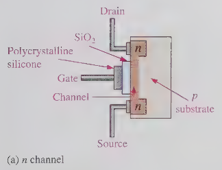
n-channel JFET
has a n-type channel and a p-type gate
the n-channel JFET is normally used with _ while p-channel JFET is normally used with _
positive supply voltages, negative supply voltages
the current through a JFET is controlled by
varying the width of the channel
there are two ways to vary the width of the JFET channel
increasing Vds while holding Vgs constant or increasing Vgs while holding Vds constant
what is pinchoff voltage (vp)
value of drain-source voltage that causes drain current to reach its maximum value at a given value of Vgs
what is shorted-gate drain current (idss)
maximum possible value of drain current for a given JFET
Idss is always measured at Vgs= _ and Vds = _
vgs = 0v and vds = vp
Id is always less than or equal to
Idss
the gate-source junction of a JFET is what biased
reversed biased
as Vgs decreases, Id _
decreases
gate-source cutoff voltage (vgsoff) is the value of vgs that causes drain current to
drop to zero
since the gate-source junction of a JFET is reversed bias, its gate input impedance is
extremely high
ability of a JFET to amplify is described as ___ and is merely the change in drain current divided by the change in gate voltage
transconductance
although voltage gain appears low in a JFET, it is almost
infinite
transconductance is indicated as Mhos or siemens and is typically what range for the MPFLOD trransisiter
2.5 mmhos - 7.5mmhos
the gate for a JFET is considered an __ and draws __ from the source
open circuit, no power
the main drawback for the metal oxide semiconductor JFET is
that the JFET gate must be reversed biased for proper operation
why does the metal oxide semiconductor have to be reverse bias?
in order to delete the channel of free carriers, thus controlling the size of the channel
the type operation for a metal oxide semiconductor JFET is refered to as
depletion-mode operation
a depletion-type device would be one that used an input voltage to do what?
to reduce the size of the channel from its zero-bias size
the metal oxide semiconductor FET, or MOSFET is a device that can be operated in the _ this means that the input signal an be used to _
enhancement mode, increase the size of the channel
the metal oxide semiconductor FET, or MOSFET is not restricted to operating with _ which makes it a _ over the JFET
its gate reversed biased, improvement
MOSFETS are very sensitive to _ due to the _
static electricity, thin layer of silicon dioxide(SiO2) a glasslike material that is an insulator
there are two basic types of MOSFET, _ and _
Depletion-type MOSFET, caled D-MOSFET, Enhancement-type MOSFET called E-MOSFET
D-MOSFET can be operated in _ where E-MOSFET can operate in _
depletion mode and enhancement mode, only enhancemenet mode
D-MOSFET has a _ between source and drain
physical channel
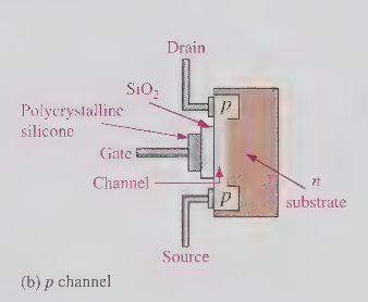
E-MOSFET depends on the _ between the source and drain terminals
gate voltage to form a channel
when the mosfet gate-source junction is reversed biased (vgs is negative) the channel is effectively reduced its
width, while increasing its resistance (same as jfet)
in mosfet initial mode, Id will be less than Idss because resistance of the MOSFET channel is
higher when Vgs is negative
when mosfet enhancement mode of operation, vgs is _ and when vgs is _
positive, positive then the channel is widened
you reduce the size in the enhancement mode of the channel and Id will be
greater than Idss
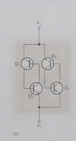
silicon controlled rectifier (SCR)
a four layer device contraining two n-type regions and two p-type regions
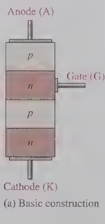
SCR is considered what type of component
a diode
SCR contains another input called
a gate
the gate in a SCR provides an additional means of _
triggering the device into the on-state
since the gate of an SCR is a approximally equivalent to a diode,
takes .7v to trigger the SCR
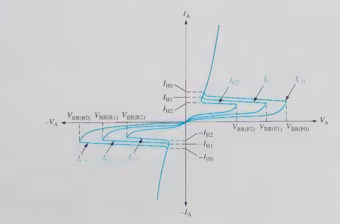
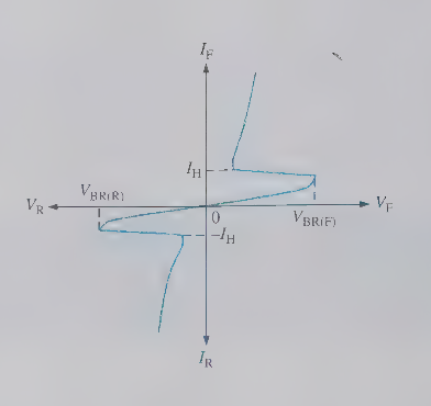
IH
holding current, minimum forward current required to maintain conduction
Itsm
non repetitive surge current, absolute limit on surge current through device
Vgd
gate nontrigger voltage, maximum gate voltage that can be applied without triggering the SCR into conduction
Dv/Dt
critical rise rating, maximum rate of increse in anode to cathode voltage that the SCR can handle without false triggering occuring
change in T
rise time of the increase in Vak
change in V
amount of change in VAK
DIAC can have _ in either direction
latch current

DIAC has _and behave essentially like a _
two-terminal bidrectional device, triac without a gate
DIAC are frequency used to trigger
traics in full-wave AC application
TRIACS acts like _
two SCR in parallel, equivalent to two latches
a TRIAC is a
3 terminal device, similar to the SCR
current in TRIAC
flows in both directions
TRIAC primary use is to
control power to AC loads such as AC motors, heating systems etc