Devices (MOSFET)
1/9
There's no tags or description
Looks like no tags are added yet.
Name | Mastery | Learn | Test | Matching | Spaced | Call with Kai |
|---|
No study sessions yet.
10 Terms
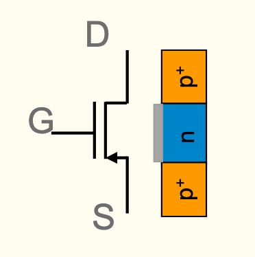
pMOS
p+np+
arrow up
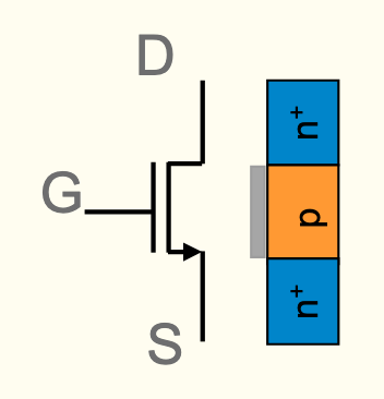
nMOS
n+pn+
arrow down
Peculiarities of MOSFET
gate (middle layer) is the 3rd contact, it has an oxide layer (serving as an insulator)
MOSFET currents rely entirely on majority carriers (of electrons in npn, or holes in pnp)
“Threshold voltage” exists to “turn on” the MOSFET and hence its pull up or pull down function
the gate has a capacitance effect which provides the carrier pathway (channel)
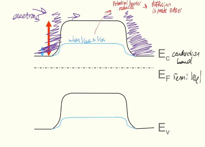
When is the channel formed?
When V(GS) = V(th), or when n(channel) = p(bulk)
(when accumulated electron concentration in p-type is equal to hole concentration in substrate p-type)
this causes a capacitance effect (Q(n) or Q(p), depending on the channel)
Current amplification (I(DS))
channel is made by inversion (pulling minorities of the middle layer up to the bottom of oxide)
thin region under the oxide becomes n-type or p-type depending on accumulation when V(GS) ≥ V(th)
When V(GS) ≥ V(th), conduction band decreases (and valence band deepens to maintain bandwidth gap)
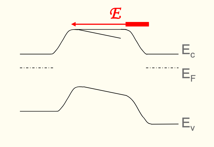
Current I(DS) when V(DS) is applied
there is a voltage drop across the channel and the channel-drain junction, this is reliant on the direction of V(DS) (and the electric field produced by V(DS))
(Assuming V(DS) is positive) the electric field produced is in the same direction as D → S, this also means for conduction and valence bands, conduction and valence bands need to shift “upward” to the end of the electric field, but the upward is caused by the end closest to the start of the electric field dropping instead
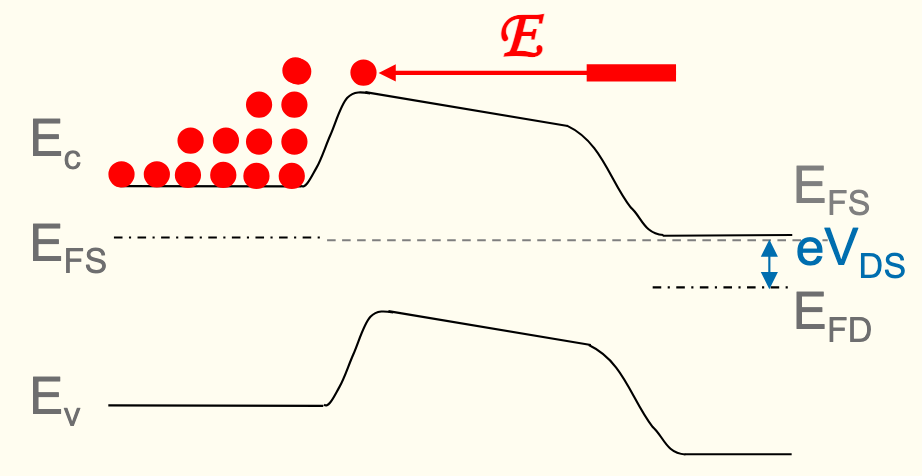
Fermi level difference between source and drain
the difference between fermi energy level of source and drain is eV(DS)
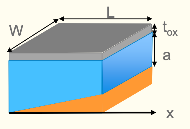
Capacitance of channel
Qn(x)=-Cox(VGS - Vth - Vx(x))
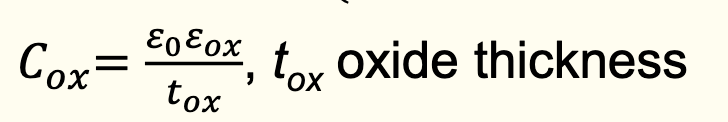
Oxide thickness
Cox= …
electron (or hole concentration)
n(x) = Qn(x) / (e*a(x))
p(x) = Qp(x) / (e*a(x))
a(x) is the depth channel