Exam 2 Semiconductor Devices and Circuits
1/88
There's no tags or description
Looks like no tags are added yet.
Name | Mastery | Learn | Test | Matching | Spaced | Call with Kai |
|---|
No analytics yet
Send a link to your students to track their progress
89 Terms
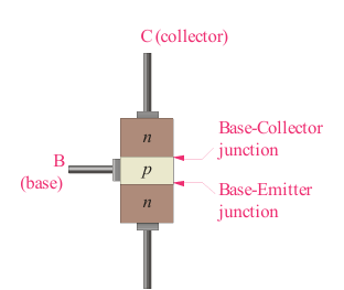
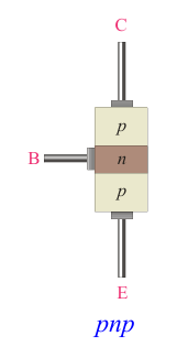
BJT (bipolar junction transistor)
a transistor constructed with three doped semiconductor regions of a BJT
Emitter
the most heavily doped of the three semiconductor regions of a BJT
Base
one of the three semiconductor regions of a BJT. The base is thin and lightly doped compared to the other regions
Collector
the largest of the three semiconductor regions of a BJT
Beta
the ratio of dc collector current to the dc base current in a BJT; current gain from base to collector
Saturation
the state of a BJT in which the collector current has reached a maximum and is independent of the base current
Cutoff
the nonconducting state of a transistor
Phototransistor
a transistor in which base current is produced when light strikes the photosensitive semiconductor base region
The region on the characteristic curve in which the current changes only slightly with an increase in VCE is called the
a. saturation region
b. cutoff region
c. breakdown region
d. active region
d. active region
βDC is defined as the ratio of
a. collector current to base current
b. collector current to emitter current
c. emitter current to base current
d. emitter current to collector current
a. collector current to base current
When a BJT is in saturation, the
a. collector current does not change with an increase in base current
b. base current cannot increase
c. collector to emitter voltage is maximum
d. all of the above
a. collector current does not change with an increase in base current
When a BJT is cutoff, the
a. voltage from collector to emitter is near zero
b. collector current is near zero
c. base-emitter junction is forward-biased
d. none of the above
none of the above
The lower end of the dc load line touches the x-axis at
a. saturation
b. cutoff
c. breakdown
d. 0.7 V
b. cutoff

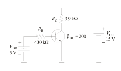
For the circuit shown, the base current is
a. 1.0 μA
b. 1.16 μA
c. 10 μA
d. 11.6 μA
c. 10 μA
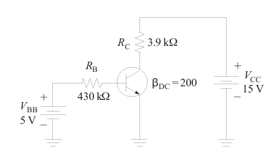

For the circuit shown, the saturation current is
a. 200 μA
b. 2.0 mA
c. 3.79 mA
d. 14.8 mA
c. 3.79 mA
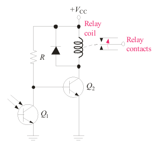
For the phototransistor circuit, assume there is sufficient light to saturate Q1. In this condition,
a. Q2 is also saturated
b. the diode is conducting
c. the relay is energized
d. none of the above
d. none of the above

An optocoupler is a single package containing
a. two transistors
b. an LED and a phototransistor
c. a phototransistor and a relay
d. an LED and a relay
b. an LED and a phototransistor
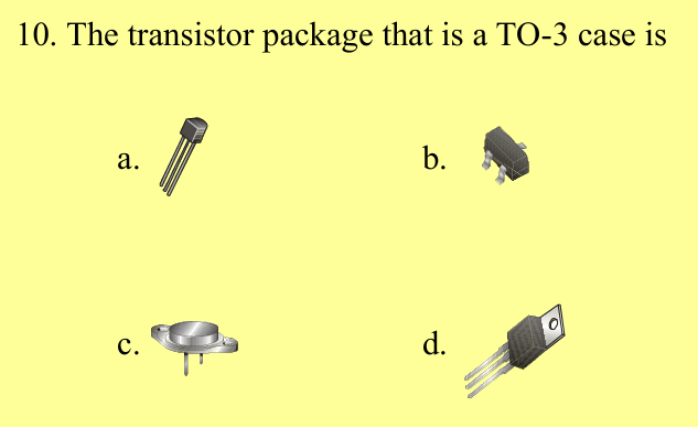
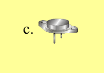
The transistor package that is a TO-3 case is
c.
BJT regions
three regions called the emitter, base and collector
BJT base
thin lightly doped region
BJT emitter
Heavily doped
BJT collector
moderately doped
npn bjt diagram
pnp bjt diagram
Normal BJT Operation
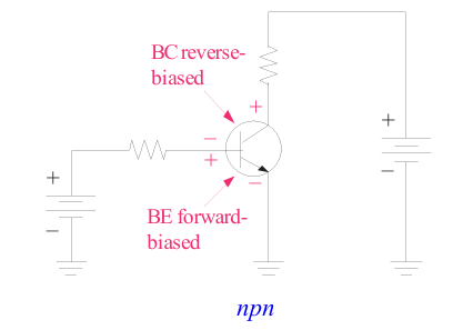
the base-emitter is forward-biased and the base-collector is reverse biased
npn BJT operation
the collector is more positive than the base, which is more positive than the emitter
pnp BJT operation
The voltages are reversed to maintain the forward-reverse bias
BJT current direction
The direction of conventional current is in the direction of the arrow on the emitter terminal
The emitter current is the ___ of the collector current and
sum
The emitter current equation
IE = IC + IB
(emitter current is the sum of the collector current and small base current)
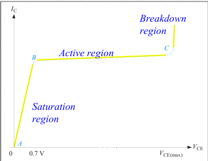
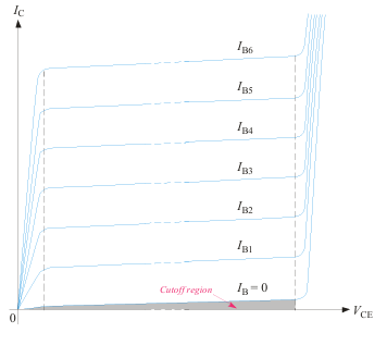
BJT Characteristics curve for fixed base current
The collector characteristic curves show the relationship of the three transistor currents
The collector characteristic curves illustrate the relationship of the three transistor currents. By setting up other values of base current, ____
a family of collector curves is developed
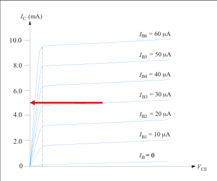
βDC is
the ratio of collector current to base current. it can be read from the curves. the value of βDC is nearly the same wherever it is read
βDC is the ratio of collector current to base current:
βDC = IC / IB

What is the βDC for the transistor shown?
Choose a base current near the center of the range - in this case IB3 which is 30 μA
Read the corresponding collector current - in this case, 5.0 mA. Calculate the ratio:
βDC = IC / IB = 5.0 mA / 30 μA = 167
BJT Characteristics for a fixed base current
The first region is the saturation region
As VCE is increased, IC increases until B
Then, it flattens in the region between points B and C, which is the active region
After C, is the breakdown region
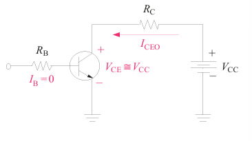
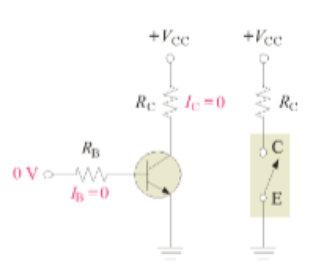
In a BJT, cutoff
is the condition in which there is no base current, which results in only an extremely small leakage current (ICEO) in the collector circuit. For practical work, this current is assumed to be zero.
In this condition, neither the base-emitter junction, nor the base-collector junction are forward-biased

ICEO
An extremely small leakage current in the BJT collector circuit in cutoff. For practical work, this current is assumed to be zero

In a BJT ___, neither the base-emitter junction, nor the base-collector junction are forward biased
cutoff
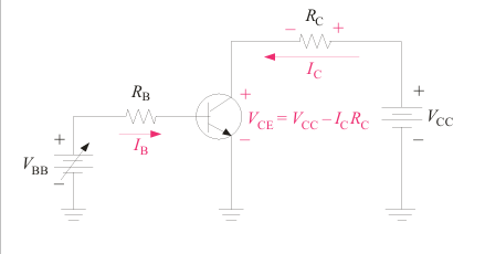
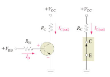
In a BJT, saturation is the condition in which
there is maximum collector current

In a BJT, saturation is determined by
the external circuit (VCC and RC ) because the collector-emitter voltage is minimum (around 0.2 V)
Why is the saturation current determined by the external circuit (VCC and RC in this case) ?
Because the collector-emitter voltage is minimum (around 0.2 V)

In saturation, an increase of base current ___
has not effect on the collector circuit and the relation IC = βDC IB is no longer valid

DC Load Line
Represents the circuit that is external to the transistor. It is drawn by connecting the saturation and cutoff points. The transistor characteristic curves are shown superimposed on the load line. The region between the saturation and cutoff points is called the active region

The transistor characteristic curves are
shown superimposed on the load line
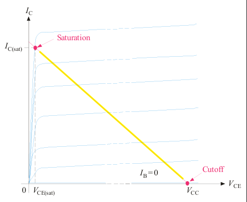

The region between saturation and cutoff points is
called the active region

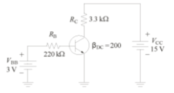
What is the saturation current and cutoff voltage for the circuit? Assume VCE = 0.2 V in saturation.
Solution:
ISAT = (VCC - 0.2 V) / RC
ISAT = (15 V - 0.2V) / 3.3kohm = 4.48 mA
VCO = VCC = 15 V
Follow-up: Is the transistor saturated?
IB = (3.0 V - 0.7 V) / 220kohm = 10.45 μA
IC = βIB = 200 (10.45 μA) = 2.09 mA
Since IC < ISAT, it is not saturated


Is the transistor saturated?
IB = (3.0 V - 0.7 V) / 220kohm = 10.45 μA
IC = βIB = 200 (10.45 μA) = 2.09 mA
Since IC < ISAT, it is not saturated

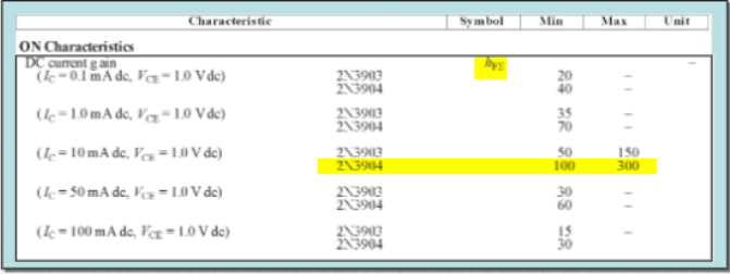
Data Sheets
Give manufacturer’s specifications for maximum operating conditions, thermal, and electrical characteristics. For example, an electrical characteristic is βDC, which is given as hFE
The 2N3904 shows
a range of β‘s on the data sheet from 100 to 300 for IC and the electrical characteristic βDC, which is given as hFE
DC Quantities subscripts
Use uppercase roman subscripts. the second letter in the subscript indicates the reference point (Ex. VCE)
Is VCE an AC or DC quantity?
DC
What does the second letter the subscript of a DC quantity indicate?
the reference point
AC Quantities and time barying signals use __ subscripts
lower case, italic (Ex: Vce)
What kind of subscript is Vce?
AC Quantity
Internal transistor resistances
indicated as lower case quantities with a prime and an appropriate subscript. Ex: r’e
What resistance does the subscript r’e show?
Internal transistor resistances
External resistances
indicated as capital R with either a captial or lower case subscript depending on if it is a DC or ac resistance. (Ex: RC and Rc)
What type of resistance does RC and Rc show?
External resistance
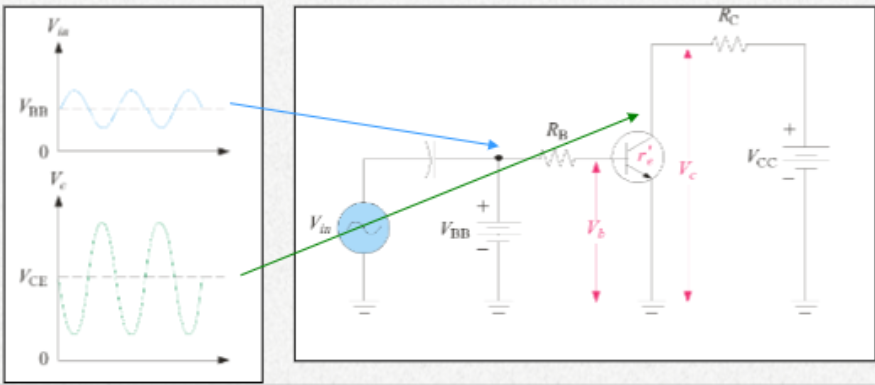
BJT Amplifiers
amplifies AC signals by converting some of the DC power from the power supplies to AC signal power. An ac signal at the input is superimposed in the dc bias by capacitive coupling. The output ac signal is inverted and rides on a dc level of VCE
A BJT can be used as a ___ in logic circuits
switching device to turn on or off current to a load
As a switch, the transistor is normally in ____
either cutoff (load is OFF) or saturation (load is ON)
As a switch, a BJT transistor in cutoff
looks like an open switch and load is OFF
As a switch, a BJT transistor in saturation
looks like and closed switch and load is ON
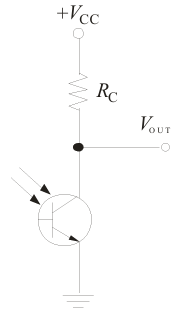
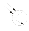
Phototransistor
produces base current when light strikes the exposed photosensitive base region, which is the active area. Has high gain and are more sensitive to light than photodiodes
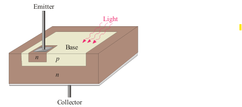
In a typical phototransistor circuit, the base lead is
left open
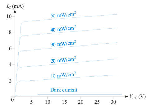
Characteristic curves for a phototransistor
based on light flux (mW/cm2) to the base rather than base current in an ordinary transistor

The output from the phototransistor can
be used to activate or deactivate a relay

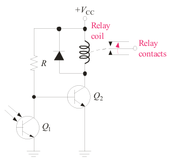
Is either transistor ON for the circuit when there is no incident light?
With no incident light, Q1 will be biased OFF. Q2 will be forward-biased through R and is ON. Collector current in Q2 causes the relay to be energized
Phototransistor Diagram
Optocouplers
A single package containing an LED and a phototransistor. They transfer a signal from one circuit to another while providing a high degree of isolation
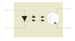
Optocoupler diagram

What do optical couplers do?
transfer a signal from one circuit to another while providing a high degree of isolation
CTR
The current transfer ratio, which is a measure of efficiency and a key specification for optocouplers. It is the ratio of output current to input current and values are typically from 50-110% for standard optocouplers
Optocouplers are used when
data or signals needs to be transferred from a control circuit to a power circuit without making electrical connections between circuits. (Ex: The logic circuits in a traffic light controller need to be isolated from the lights themselves)
An application for optocouplers is
as a transducer to detect a light path such as a hole in a rotating disk
Optocouplers are useful for
isolating patients from the monitoring instruments
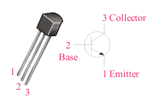
TO-92 transistor
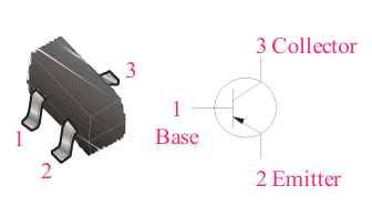
SOT-23 transistor
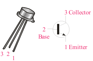
TO-18 transistor
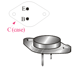
TO-3 transistor
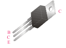
TO-220AB Transistor
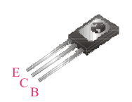
TO-225AA
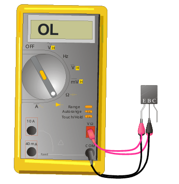
BJT Basic Test
Use the Diode Test function of your DMM.
To test the base-emitter junction of a BJT, connect the positive lead to the base and the negative lead to the emitter.
You should see a voltage close to 0.7 V for an npn transistor.
Reversing the leads will show OL for “overload”
The procedure is repeated to test the base-collector junction