3B5 General
1/101
There's no tags or description
Looks like no tags are added yet.
Name | Mastery | Learn | Test | Matching | Spaced | Call with Kai |
|---|
No analytics yet
Send a link to your students to track their progress
102 Terms
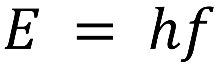
Photon energy equation?
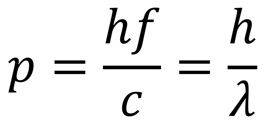
De Broglie relations?
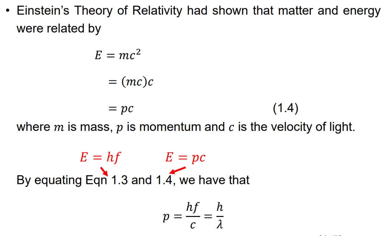
Derivation of de Broglie relation?
When does constructive interference occur?
When path difference is nλ —n is integer
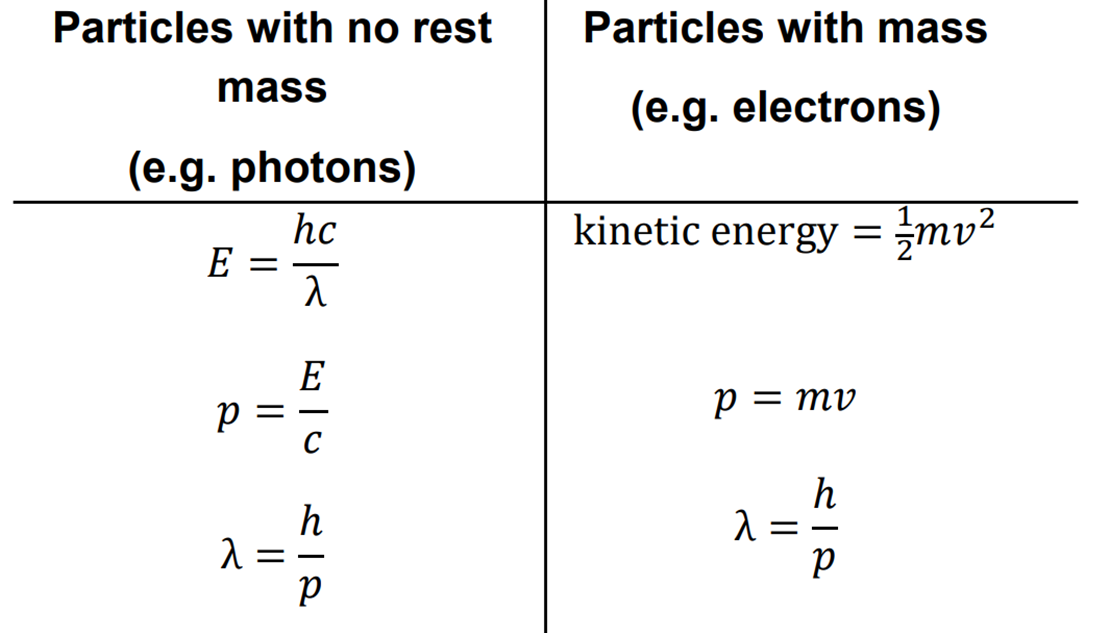
Energy, momentum and wavelength of photons vs electrons?
Alternative expression for kinetic energy of electron?

What is the purpose of the Schrodinger equation?
can determine the correct shape of the wavefunction in the presence of external forces or potentials as a function of time
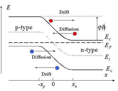
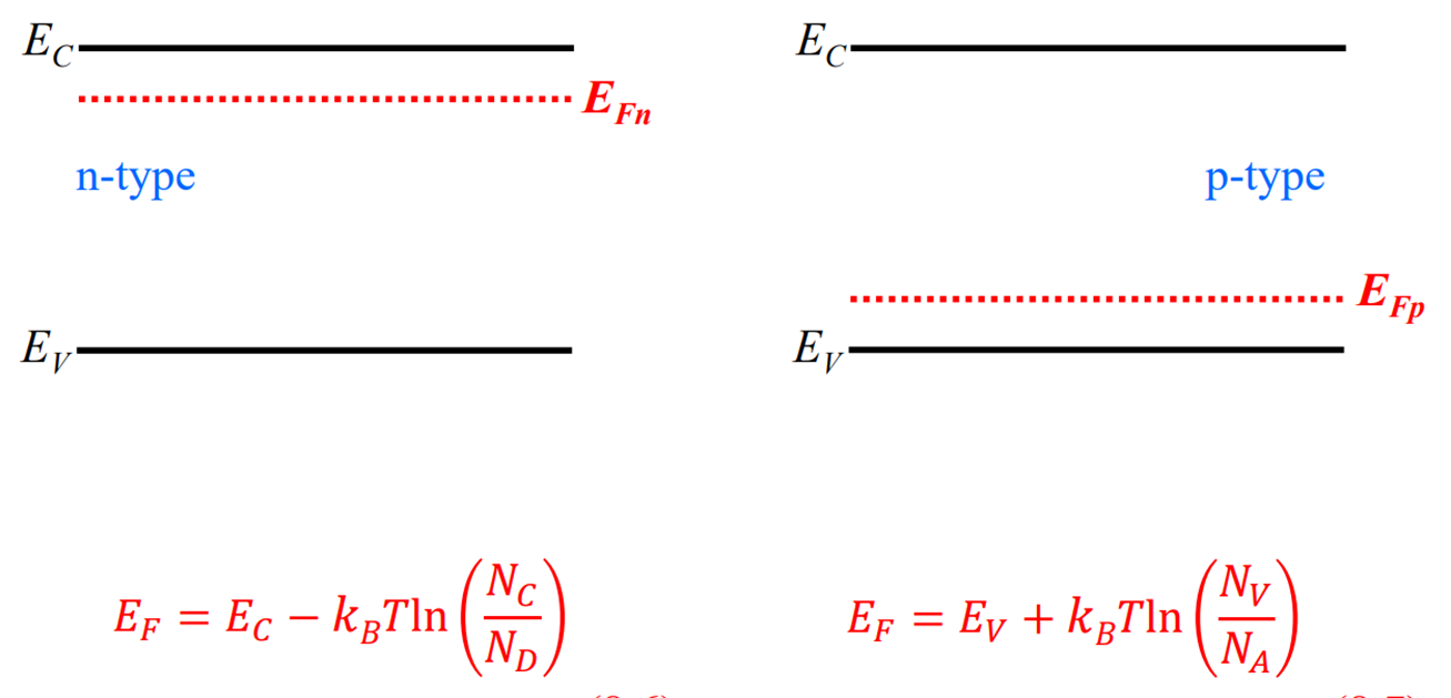
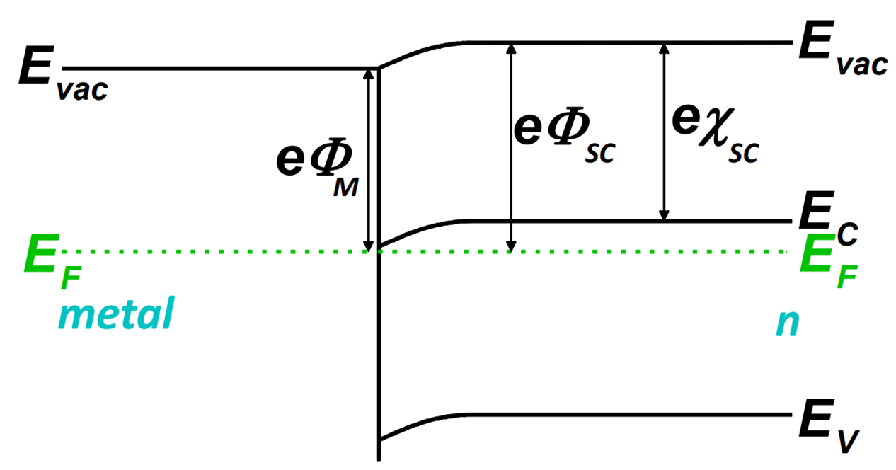
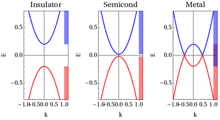
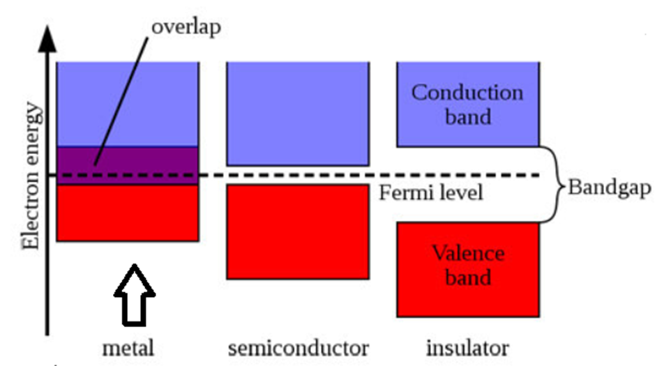
How does an equilibrium band diagram differ?
Fermi level is constant (straight line)
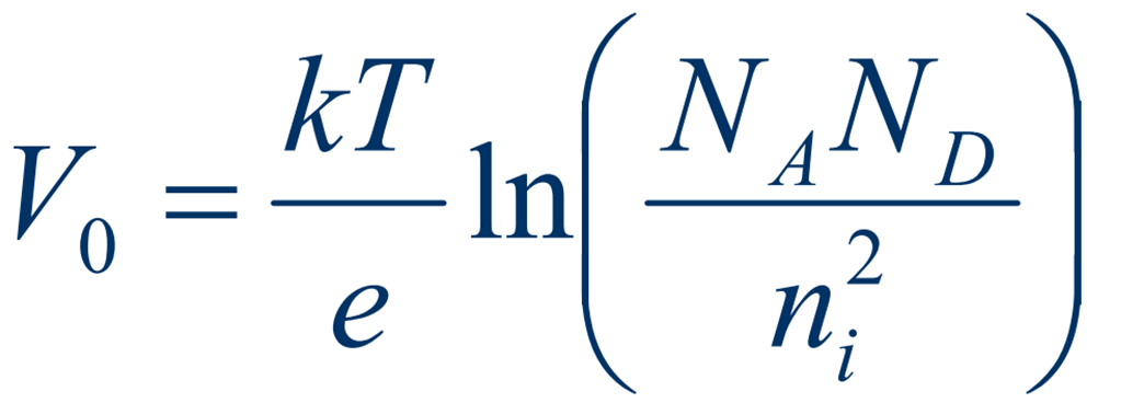
Equilibrium contact potential equation?
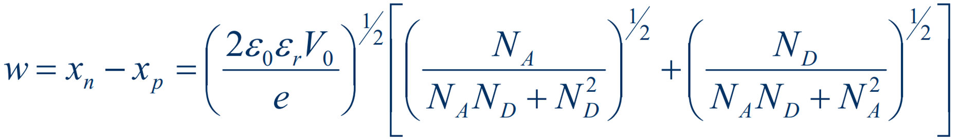
Total width of junction equation?
Why does depletion region in p-n junction essentially act as capacitor?
depletion region contains NO mobile carriers
therefore insulating
therefore acts as capacitor
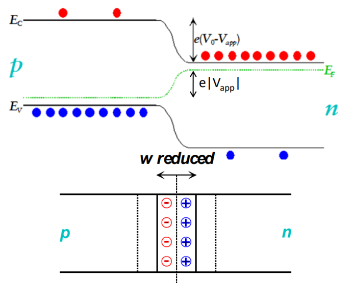
What is forward bias of p-n junction?
+ve voltage to p-side
What happens when you apply +ve voltage to p-side of p-n junction?
Energy of n-side electrons increases
Energy of p-side electrons decreases
EF lower on p-side
depletion width, barrier, peak field reduced
capacitance increased (because of depletion width)
What happens when you apply -ve voltage to p-side of p-n junction?
Energy of p-side electrons increases
Energy of n-side electrons decreases
EF higher on p-side
depletion width, barrier, peak field increased (easier to go p-side to n-side than n-side to p-side now)
capacitance decreased (because of depletion width increase)
Visual representation of why depletion width is wider on lower-doped side of p-n junction?
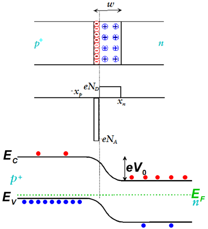
Wider on the lower-doped side because fewer charges, so depletion region extends further into that side to balance the same total charge from other side
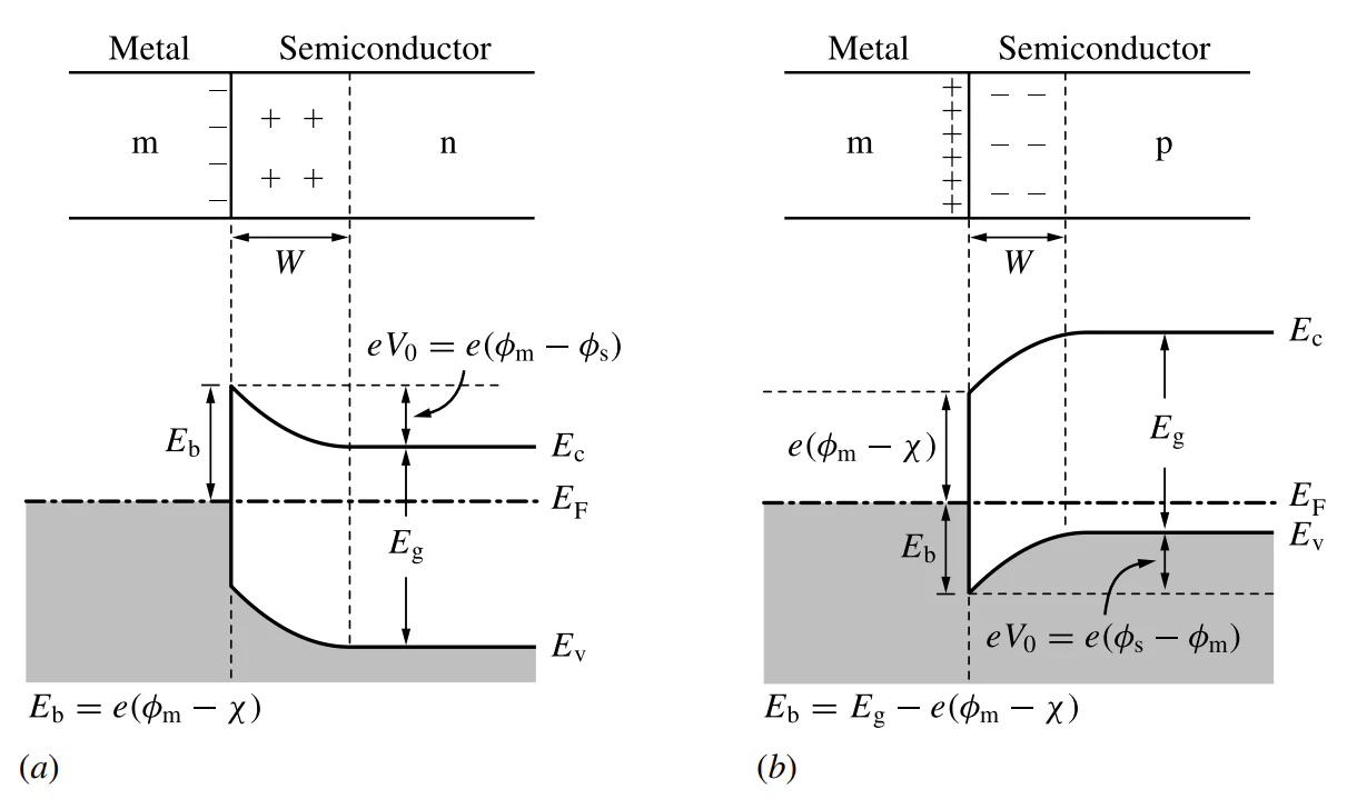
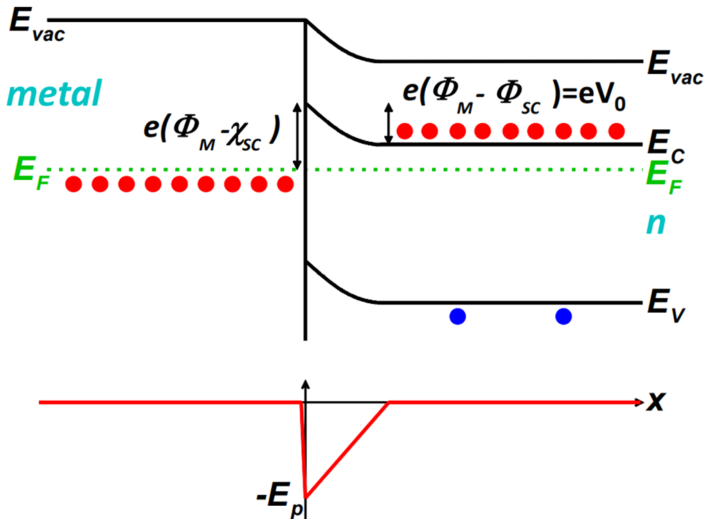
Condition for Schottky Barrier for n-type semiconductor in contact with metal?
And all other conditions that follow?
n-type & metal
Φm > ΦSC → Schottky Barrier
Φm < ΦSC → Ohmic Contact
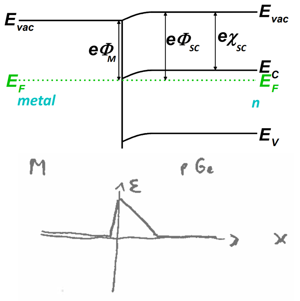
p-type & metal
Φm < ΦSC → Schottky Barrier
Φm > ΦSC → Ohmic Contact
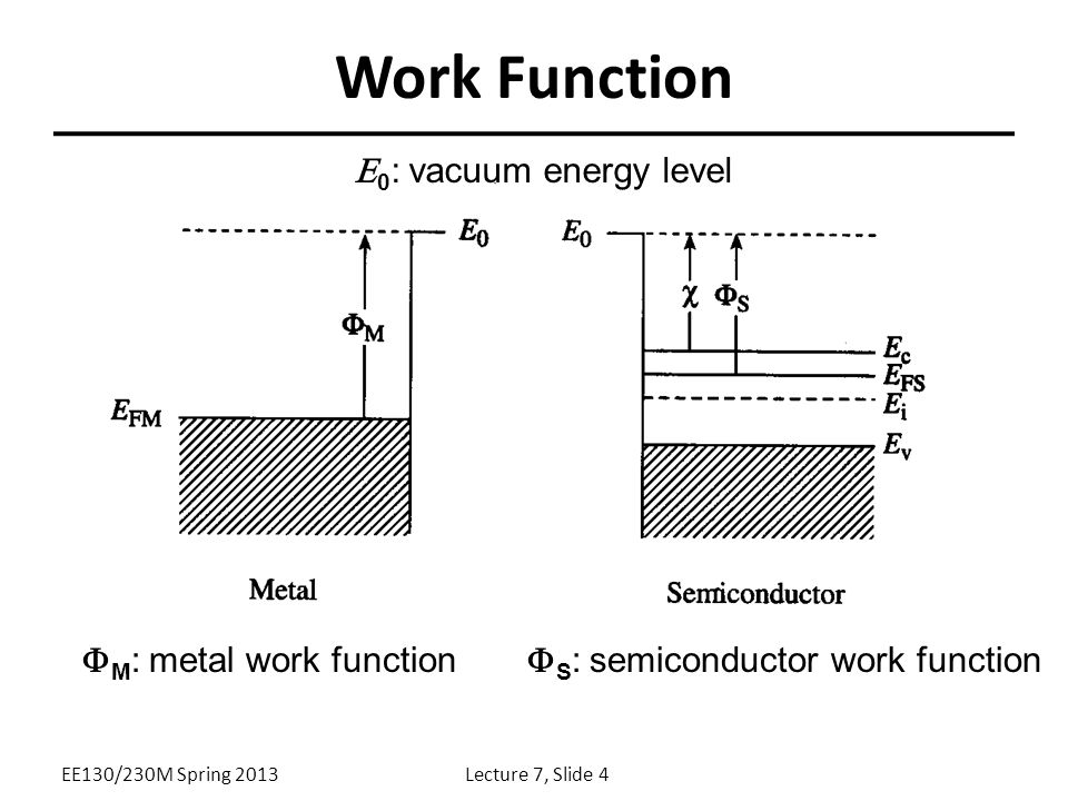
What is Φ measured between?
Φ = Evac - EF

What is affinity, X, measured between?
X = Evac - EC
What’s a heterojunction?
interface between two layers or regions of different semiconductors
Heterojunction band diagram?
pn junction band diagram?
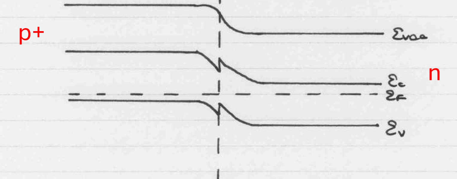
Heterojunction EF assumptions?
p+ : EF - EV ≈ 0
∴ Φ ≈ Evac - EV
n : EC - EF ≈ 0
∴ Φ ≈ X
What is the aim of n-type doping?
increase number of electrons in CB (conduction band)
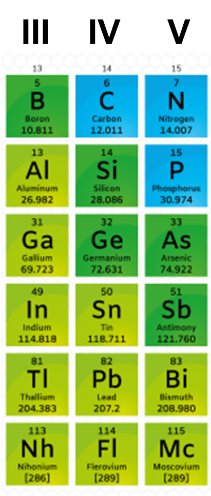
Which group do we add as donor dopants to n-dope a group IV element (e.g. silicon)?
And examples of common dopants?
group V (5 electrons—1 extra electron)
phosphorous
arsenic
antimony
Which group do we add as acceptor dopants to p-dope a group IV element (e.g. silicon)?
And examples of common dopants?
group III (3 valence electrons—1 extra hole)
boron
aluminium
gallium
Equation relating dopant densities and number of electrons?
n = ND - NA
EV in p-type semiconductor?
EV = 0 eV
(defined for convenience)
p-type vs n-type Schottky barrier?
Equation for energy of electron in a state?

What energy does the equation E=eV represent?
Energy gained by electron when accelerated across a potential difference
Experimental evidence for Einstein postulate E = hv?
Photoelectric effect
Max energy of electrons emitted from metal surface in vacuum linearly increases with photon frequency, suggesting that E = hv
[increasing intensity linearly increases number of photons per second, hence number of electrons emitted per second]
Experimental evidence for de Broglie postulate, λ = h/p?
Electron diffraction
Beam of electrons incident on regular crystal structure metal sample, diffraction pattern with peaks formed when constructive interference due to this angle:
nλ = 2 d sinθ
with λ = h/p
Probability postulate for Schrodinger’s equation?
Probability of finding the particle is |Ψ|2
Total integrated probability over all space is 1
∴ ∫0L |Ψ|2 dx = 1
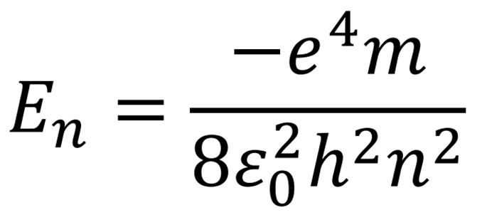
Equation for energy of electron in one electron system?
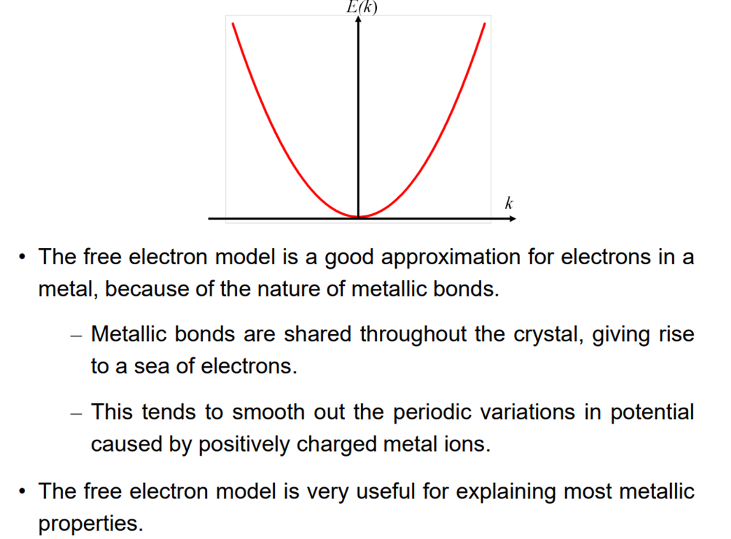
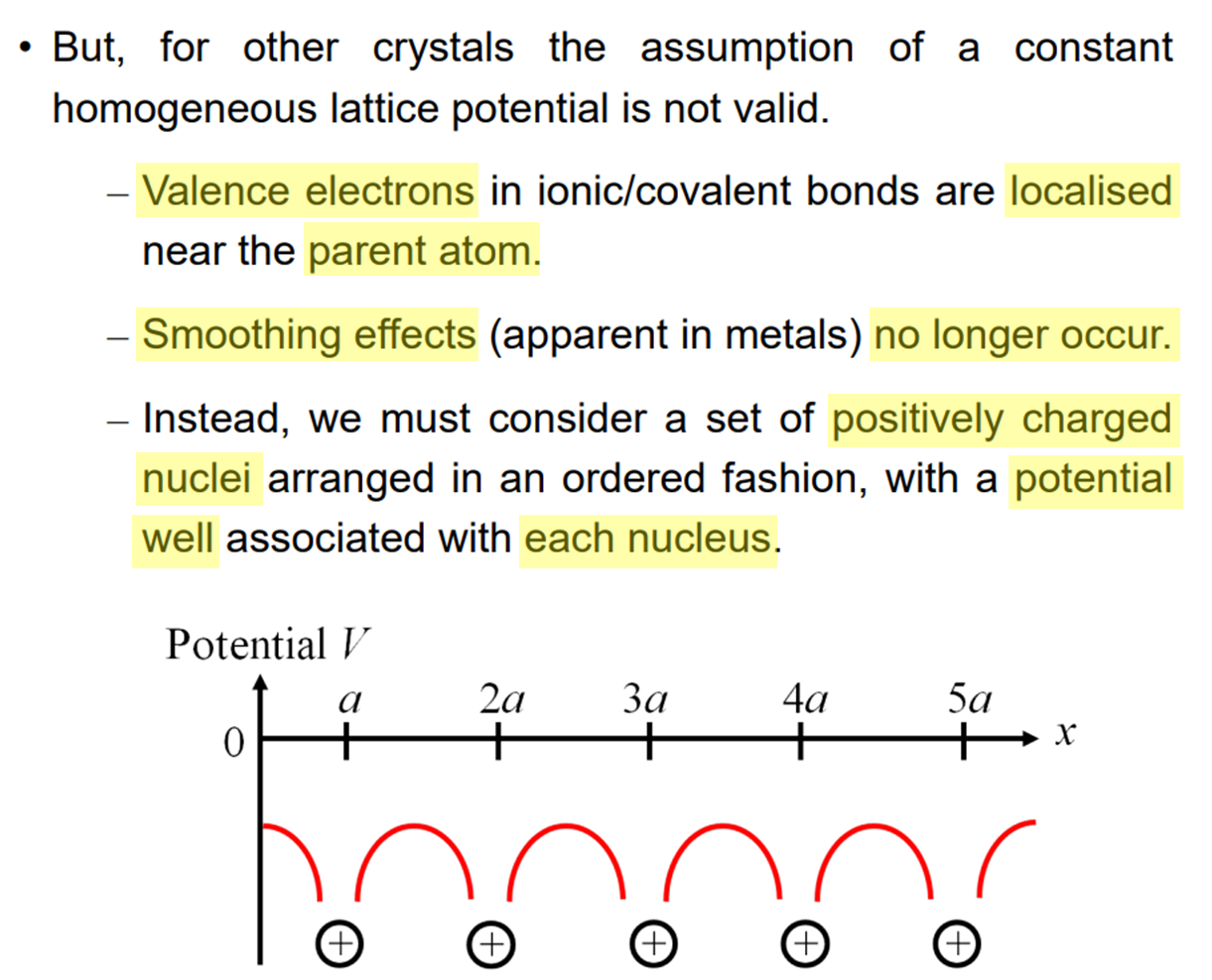
Assumptions of free electron model?
Electrons in the solid behave like a gas of free particles (free to move)
Removal of valence electron to be free carrier leaves behind a positively charged ionic core—charge density of these ionic cores is spread uniformly through the solid (with potential V0)
No interaction between free electrons
E-k equation?
And when can you use this?
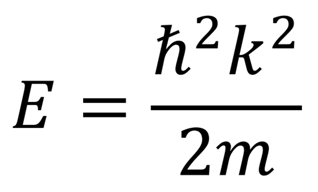
Only for 1D
(also you can use with m*)
What do the spherical shells in k-space represent?
Wavevectors with the same magnitude and ∴ same energy
Same wavenumber (k) —2 electrons at each point
Find number of states between k and (k + dk) with |k|?
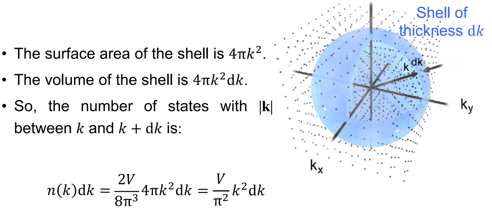
Number of states in volume × volume of shell
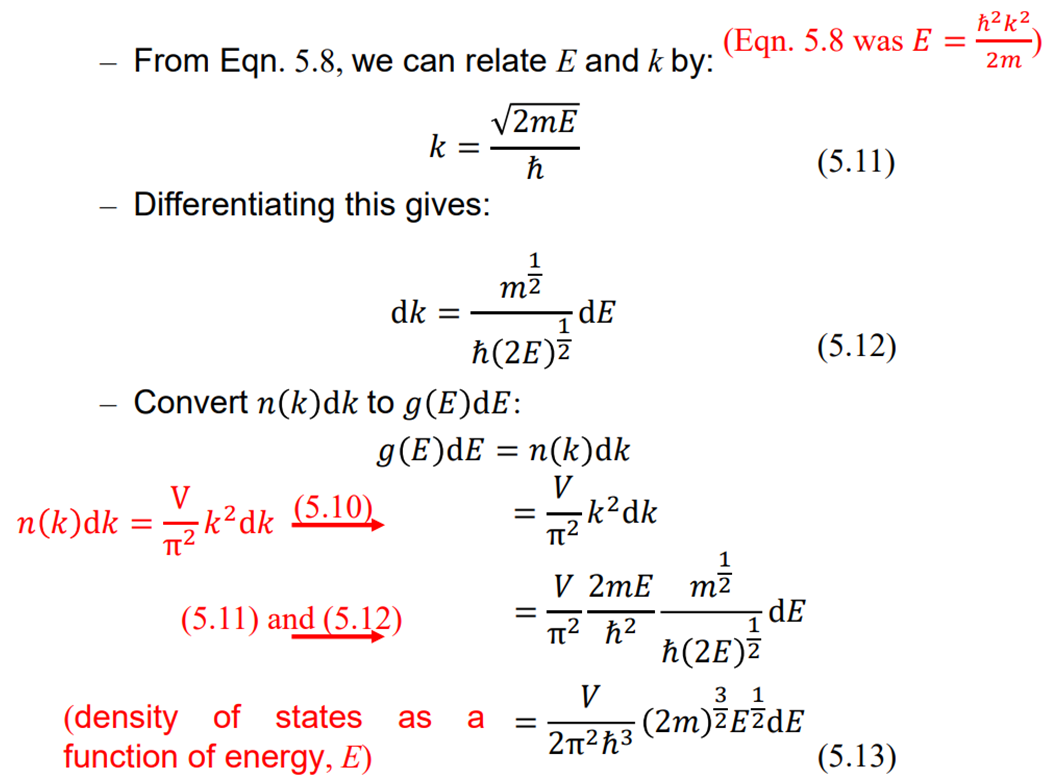
How to derive g(E) dE?
Why is free electron model good for metals but not other crystals?
In a non-metal crystal, when will the electron propagate as a travelling wave and when will it not?
λ doesn’t meet Bragg reflection criteria:
-travelling wave
-solution from free electron theory will apply to a first approximation
λ does meet Bragg reflection criteria
-wave becomes standing wave ‘locked on’ to periodicity of the lattice
-electron can’t propagate as travelling wave through crystal
-solution from free electron theory will not apply
For which wavenumbers does Bragg reflection occur?
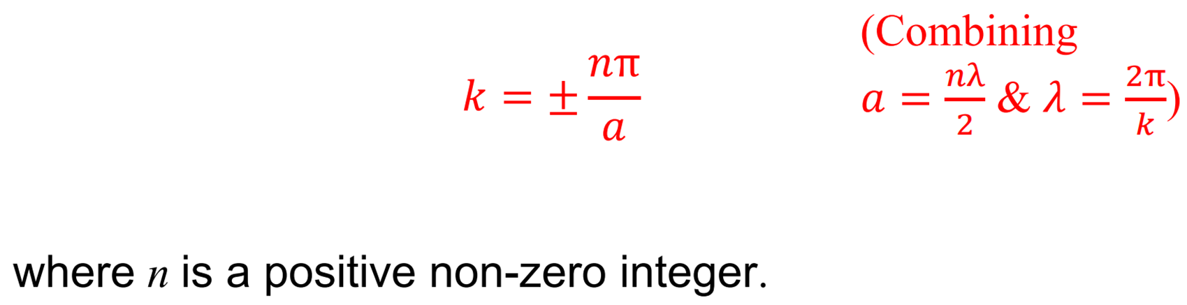
What is Bloch’s theorem? How does this change the E-k diagram (Brillouin zones)
For a periodic potential, V(x) = V(x + Na)
Solution to the TISE is a plane wave multiplied by a function with the same periodicity as the lattice: Ψ = 𝐴 exp(j𝑘x) u(x)
Impossible to distinguish between electron with wavenumber k and one with wavenumber k+n2π/a
∴ can move any point on E–k diagram by ±n2π/a without changing the physical significance
Can condense all information in E–k diagram into 1st Brillouin zone
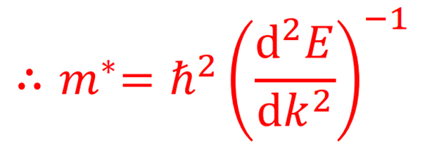
Equation for effective mass of electron?
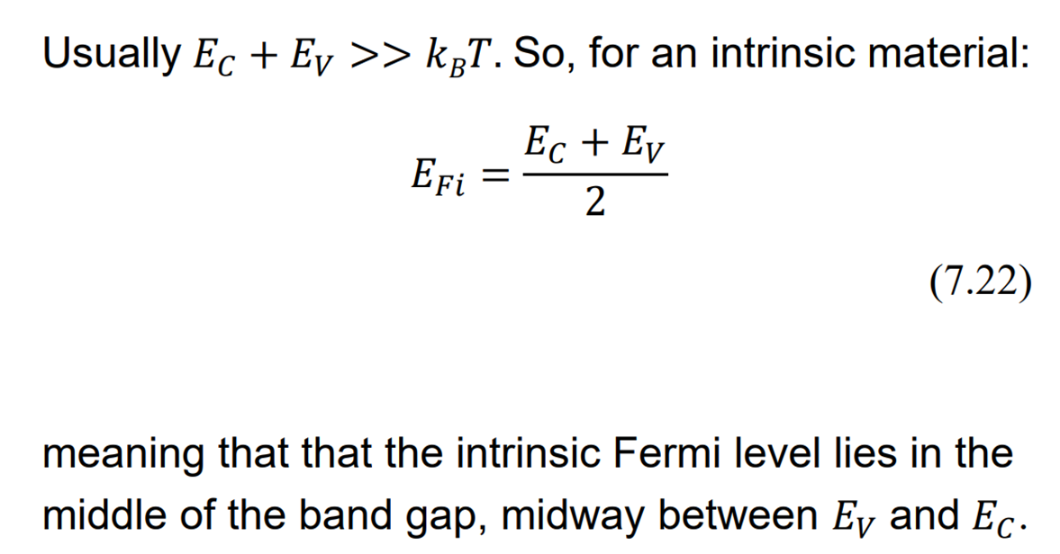
Where is the intrinsic Fermi level?
Intrinsic material:
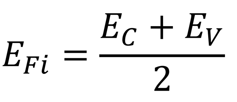
halfway
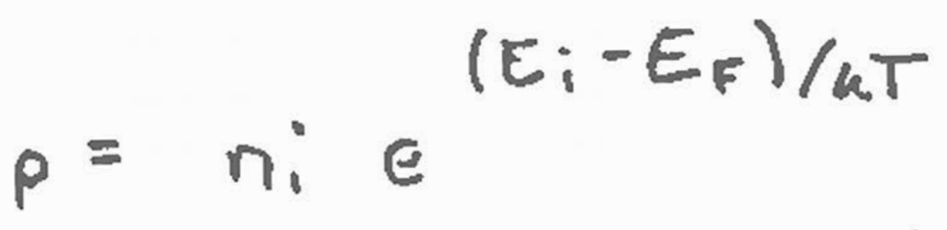
Derive intrinsic Fermi level, derive law of mass action, derive Nc and Nv
Equations for how doping changes the Fermi level in p-type and n-type?
Will you get up and read 2023 Q1 crib right now?
Yes
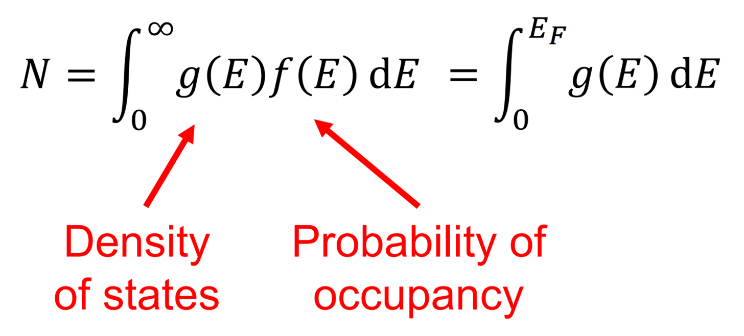
What is N and how do you find it?
N = states occupied
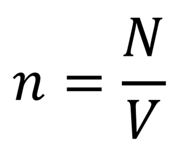
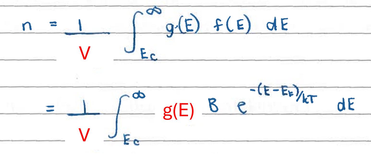
What is n and how do you find it?
n = number density of free electrons
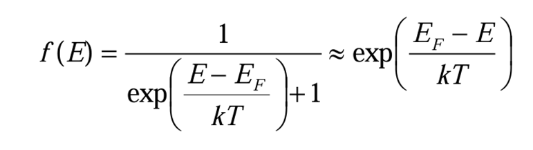
How to find probability that a state is occupied when we have a limited number of states due to the Pauli exclusion principle?
Fermi-Dirac distribution
When can Boltzmann approximation to the Fermi-Dirac be used?
E >> EF
OR
EC - EF >> kBT
Probability that a state is occupied is very low → finite number of states is no longer the factor limiting occupation
For which semiconductors is direct recombination most likely?
Semiconductors with direct band gaps
For indirect gap: electron must lose energy and dissipate momentum (the creation of a phonon)
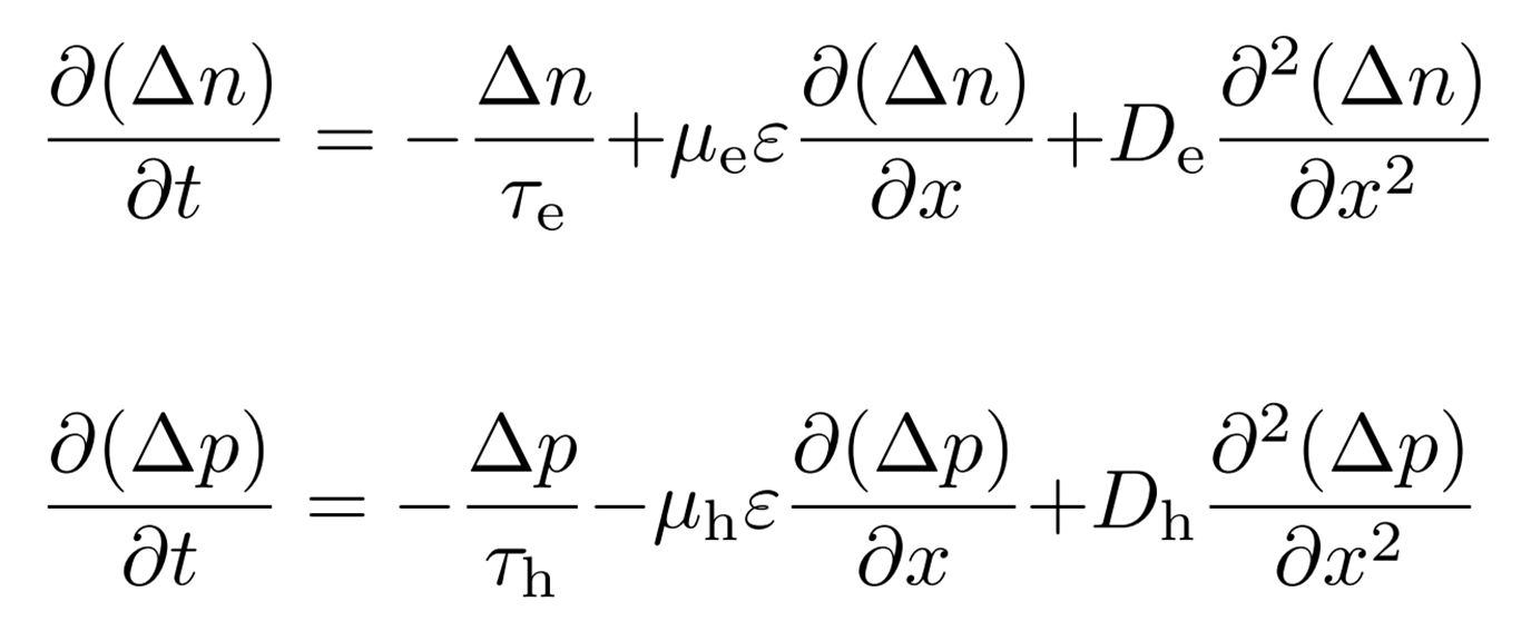
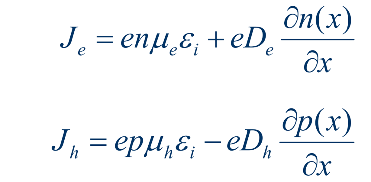
What does each part of the continuity equation represent?
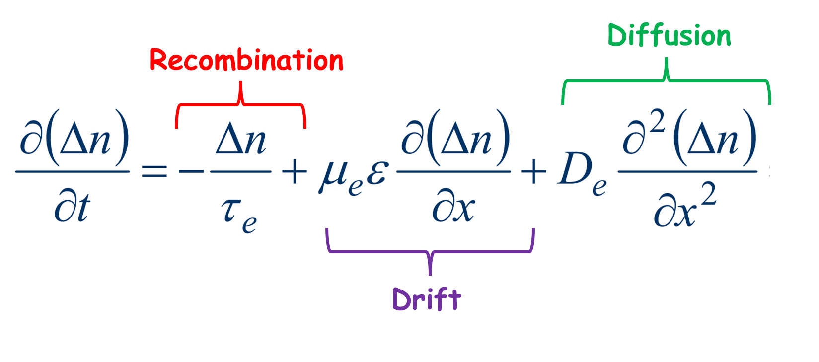
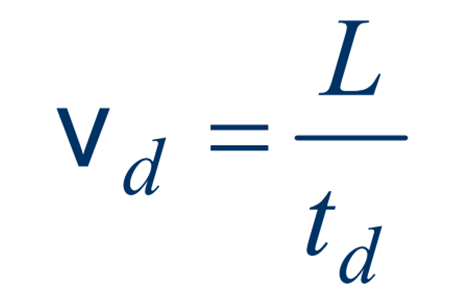
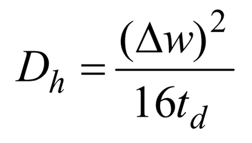
Haynes-Shockley experiment?
Pulse of holes (minority carriers) created in n-type bar (e.g. laser)
Electric field applied
Pulse drifts in field and spreads out by diffusion
Drift mobility of holes = from run time
Diffusion coefficient = from pulse broadening
Hole lifetime = from total decay of carriers
Haynes-Shockley gives minority carrier mobility
Hall effect gives majority carrier mobility
Drift and diffusion for majority/ minority carriers?
DRIFT = only for majority
DIFFUSION = minority carriers have great effect
Reason why EF might be above midway point in intrinsic semiconductor?
NV > NC
In n-type and p-type doping, where are the extra electrons and holes desired?
n-type: increase electrons in CB
p-type: increase holes in VB
What is electron affinity?
energy required by electron at bottom of CB to escape from semiconductor into vacuum
In n-type Schottky barrier diode, which barrier is fixed, and what is its value?
Which barrier varies, how does it vary, and what is its value?

Fixed barrier: e(ϕm - Xsc)
electron flow from M to SC
Variable barrier: e(ϕm - ϕsc)
electron flow from SC to M
varies with applied bias
Draw Schottky barrier band diagram?
And way to remember?
And metal and semiconductor band diagrams separately?
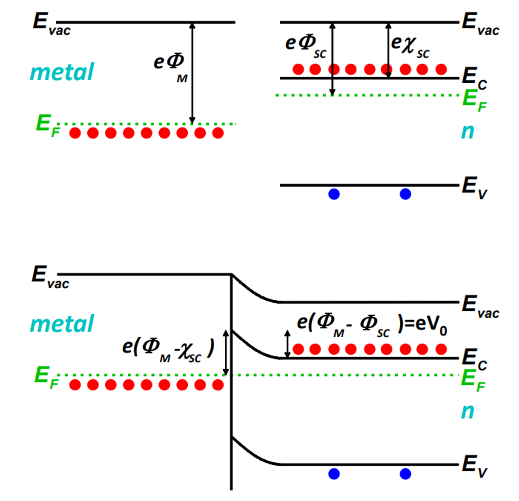
SC pulled down ↓ (yoink)
N-type Ohmic contact band diagram?
And way to remember?
SC pulled up ↑(yank)
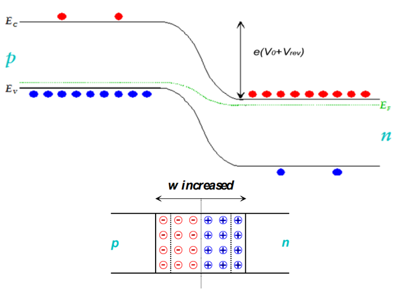
N-type Schottky barrier diode with forward and reverse bias?
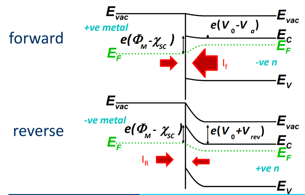
Reverse: barrier for electrons from SC to M is higher → e(V0 + Vrev)
NMOS vs PMOS?
NMOS: electrons carry current between S & D
PMOS: holes carry current between S & D
How does MOSFET work?
Voltage applied to gate
Induces Electric field in gate insulator
^ extends into S-D channel
Changes in this E field cause modulation in resistivity of semiconductor underneath gate insulator
∴ V on gate can control current between S & D
What is MOSFET depletion mode?
transistor normally ON
current between S & D
until V (of appropriate magnitude) turns it off
[like JFET—typically in depletion mode, but MOSFET can do both. get you a girl who can do both]
What is MOSFET enhancement mode?
transistor normally OFF
no current between S & D
until sufficiently large threshold voltage applied to gate
Is enhancement or depletion MOSFET better for energy saving?
normally OFF i.e. enhancement
Band diagram of n-type
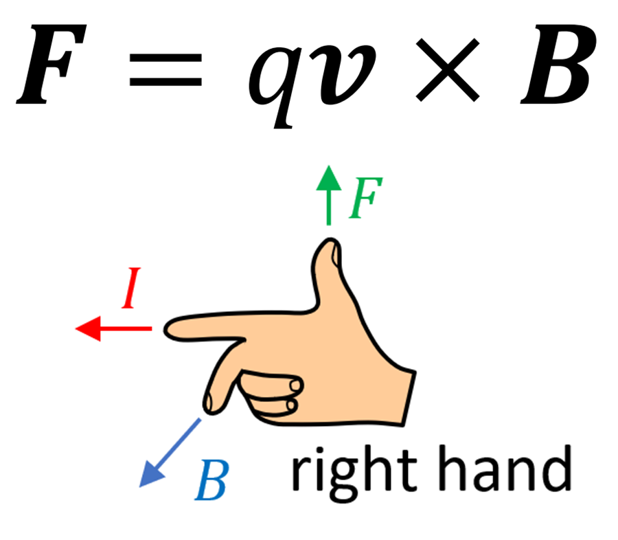
Lorentz force equation?
And hand rule?
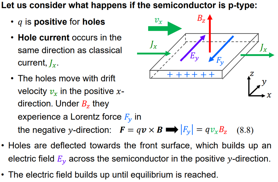
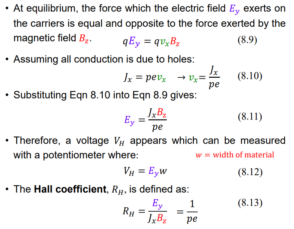
Hall effect explanation in p-type semiconductor?
And derive Hall coefficient?
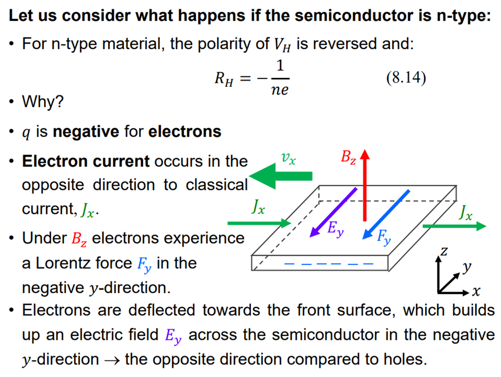
Hall effect explanation in n-type semiconductor?
And derive Hall coefficient?
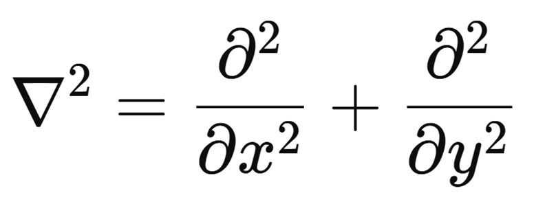
What is the Laplacian, ∇2, equal to?
[in maths DB]
Important to remember when differentiating TISE solution?
j comes down to front!!
Quick equation to find (dk what to call it but example 9.A eqn)
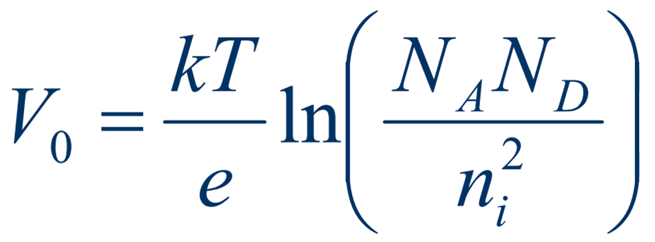
Equation for electrostatic potential difference between 2 side of pn junction (i.e. contact potential)?
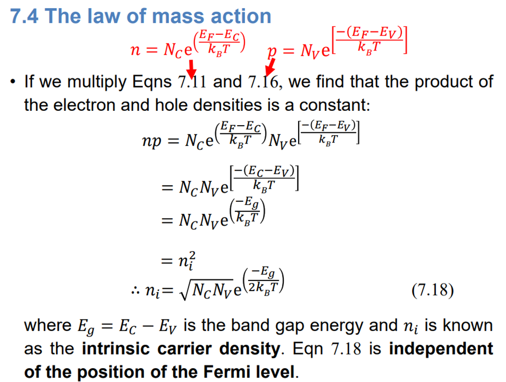
Prove the law of mass action?
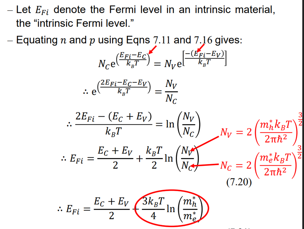
Prove intrinsic Fermi level position?
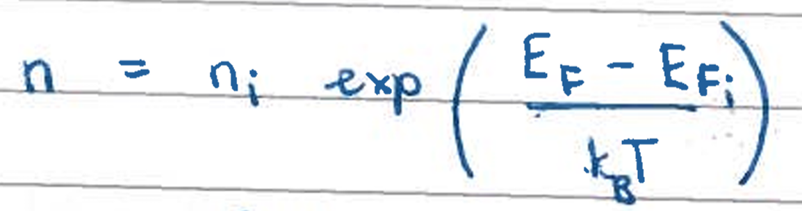
Equation to find Fermi level with respect to intrinsic Fermi level using ni (for n-type and p-type)?
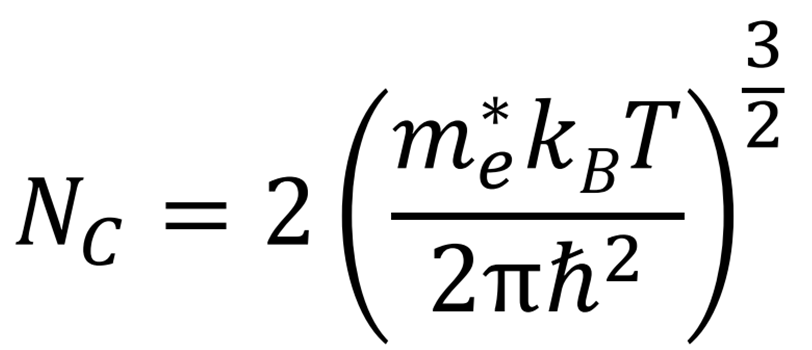
Equation for effective density of states in CB?
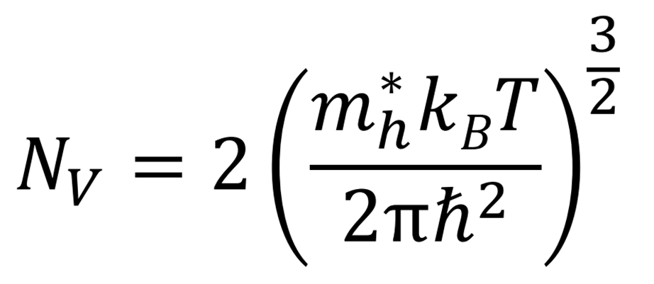
Equation for effective density of states in VB?
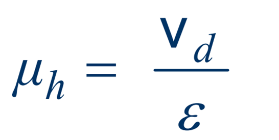
Units of mobility?
m2 V-1 s-1
How to determine direction of Hall voltage?
Find direction of Fy
holes/ electrons build up at surface that Fy points to
Ey in +ve to -ve direction (towards e, away from h)
VH in opposite direction to Ey (voltage always decreases in applied E field direction)
Groups III, IV & V of periodic table?
Semiconductor Arrhenius plot regions and explanations?
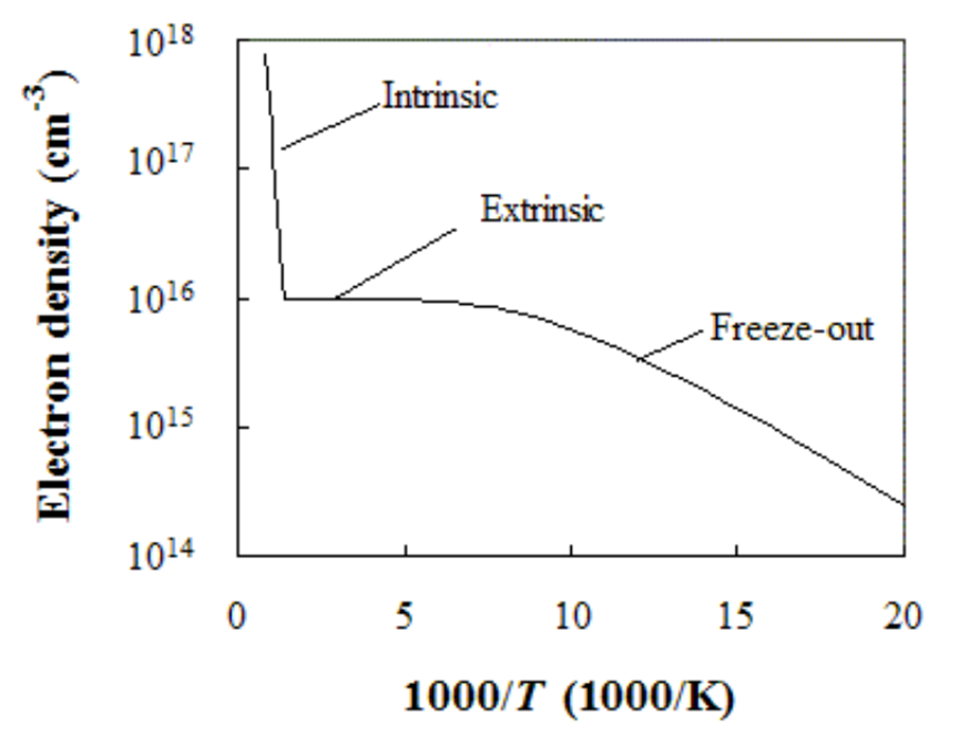
0K: no carrier in any band, no ionised dopants —behaves like insulator
Small temp rise: donor impurities begin to ionise (some electrons in CB)
Flat region: all donors ionised, saturation region. Extrinsic conduction dominates
High temps: sufficient thermal energy for electrons VB → CB. Intrinsic conduction dominates
Bandgap and Arrhenius plot relationship?
Intrinsic region (left hand side): slope α Eg
Is de Broglie for photon or electron?
TRICK QUESTION! It’s both ;)
Band diagram and Fermi level of metal?
3 Haynes-Shockley equations?
What is ρ in the Poisson equation?
And what is it equal to?
charge density due to ionised acceptors on p-side: -e NA
due to ionised donors on n-side: e ND
What does ND>>ni imply?
heavy n doping
Have you reviewed 2024 Q1?
yes, ma’am
Band diagram when there’s an internal electric field but no current flow (as drift is balanced by diffusion)?
And why would there be an internal electric field?
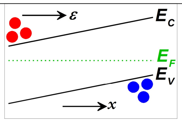
ND varies with position
How to do drift and diffusion current balance (both holes and electrons)?
How to draw E-field variation for Schottky/ Ohmic for both n- and p-type?
summary: triangle on bending side
also gradient on non-bending side
up triangle if yank (up)
down triangle if yoink (down)
Band diagram and depletion width of forward-biased p-n junction?
Band diagram and depletion width of reverse-biased p-n junction?
Frequency of LED light at T = 0 K vs at T > 0 K ?
T=0K : LED would emit light with frequency corresponding to the band gap: hf=Eg
No thermal energy is available to excite electrons to CB
Electrons recombine exactly across the band gap
All photons have the same frequency
T>0K : thermal fluctuations broaden the spectral width of the emitted light
Thermal energy is available: electrons and holes gain random K.E
Don’t always recombine exactly at CB boundary
Emitted light isn't a single frequency anymore — it’s broadened into a small range
Frequency uncertainty is Δf= E / h
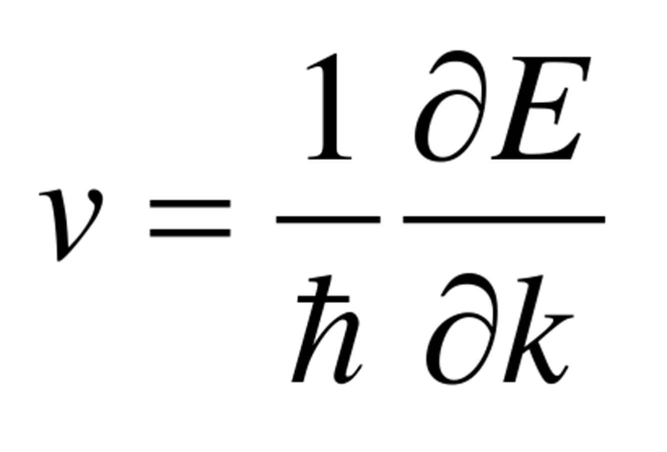
Equation for group velocity?
VB at 0K?
Fully occupied
Electrons want to be in lowest possible energy states because no thermal energy to excite them
No electrons have enough energy to jump across bandgap