Semiconductors
1/103
There's no tags or description
Looks like no tags are added yet.
Name | Mastery | Learn | Test | Matching | Spaced | Call with Kai |
|---|
No analytics yet
Send a link to your students to track their progress
104 Terms
what is a feature of a conductor regarding their atomic structreq
less than 4 electrons in its valence band
this overlaps with the conduction band
what is a insulator
a material with no free electrons
What is a diffrence between conductors and a semi conductor
a semi conductors valence shell does not overlap with conductors
what is doping
adding very small amounts of a different element with either more, or less electrons in its outer shell.
what is the process of doping
an impurity is introduced into the semi conductor in order to change its electrical conductivity
it allows it to act like either a semi conductor or in insulator
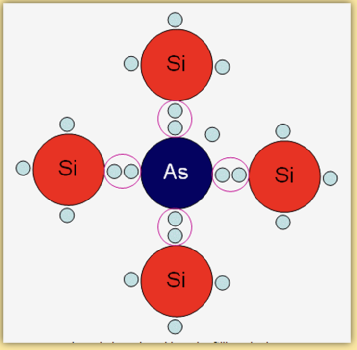
N type conductor what is it.
add a small number of atoms aresenic (As) with five outer electrons in its outer shell to pure silicon with four. we end up with a spare electron in the conductor layer.
because atom can have 8 in this band because its silicon and we bond them we would have an extra electron this process is what doping is
we do this because that free electron can now carry charge make it N(egative) type
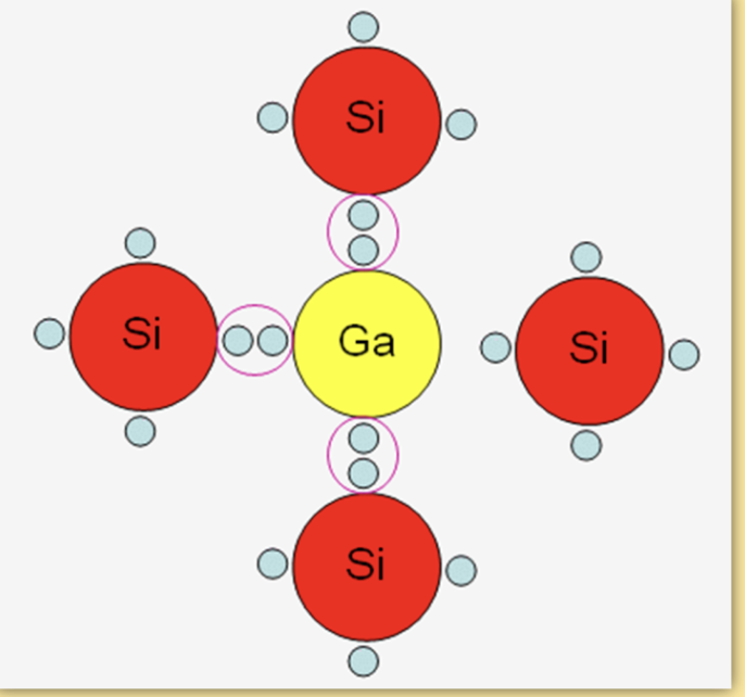
What is a P type semi conductor
now beacause silicon has four outer electrons if we add something like gallium with 3 outer electrons gives 7 not 8 outer electrons leaving a hole that can attract electrons
this creates electric current
P(ostive) type
what happens if we attach a piece of P type to a piece of N type
we get a “depletion layer” because its depleted of free charge carriers
what is a diode and its property
n type joined to p type doped semi conductor
its fundamental property is to conduct electric current in only one direction
how can we use the diode and how does it work
force current in one direction by reinforcing/eliminating the depletion layer can flow across the diode
what is a transistor
two diodes using three layers of semi conductor
what if we apply two different power supplies with enough voltafe to a two diodes
becomes transistor which functions as an electron switch
how can we use semi conductors to create a switch
we need three layers of them
what is a photodiode
a semi conductor that converts light into electrical current
the current is generated when photons are absorbed by the photodiode
the light energy creates a hole within the depletion layer which allows current to flow
at night what does the photodiode do
its semiconductor acts as an insulator and at day its a conductor
what is CCDs
2d rays of photodioded that chanhe light into a grid of electrical charge
all of the photodiode is a pixel. so more light on it means more charge created
what must we do to the charge in photodiode to make it useful
moved to main memory using a shift byte by byte
Semiconductor
Materials that conduct electricity at values between that of a pure metal and a good insulator.
Doping
The process of adding impurities to pure semiconductors to enhance their conductivity.
N-Type
Materials with negatively-charged carriers (free electrons) due to the presence of donor impurities, determining conductivity.
P-Type
Materials with positively-charged carriers ("holes") due to the presence of acceptor impurities, determining conductivity.
P-N junction diode
Formed by joining a P-Type semiconductor to an N-Type semiconductor, creating a single semiconductor-crystal structure.
Magnet
Any material or object that produces a magnetic field.
Magnetic Field
A volume of space where magnetic forces are exerted.
Law of Magnetism
Like poles repel, unlike poles attract.
Magnetization
The process where a magnetic material acquires magnetism, either temporarily or permanently.
Electromagnet
A current-carrying conductor wrapped around an iron core.
Magnetic Flux
The number of lines of force in a magnetic field (φ).
Magnetic Flux Density
The number of lines of force per unit area in a given magnetic field (B).
Neutral Point
The point between magnetic fields where magnetic flux density is 0.
Angle of DIP
The angle between Earth's magnetic flux and the horizontal.
Angle of DECLINATION
The angle between magnetic North and geographic North.
What is the relationship between temperature and carrier concentration in intrinsic semiconductors?
Carrier concentration increases with temperature due to more electron-hole pairs being generated.
What are majority and minority carriers in semiconductors?
Majority carriers are the most abundant type of charge carrier in a doped semiconductor (electrons in n-type, holes in p-type), while minority carriers are the least abundant.
Define the term "acceptor" in the context of semiconductors.
An acceptor is an impurity atom that increases the number of holes (p-type).
What happens to the conductivity of an intrinsic semiconductor as temperature increases?
The conductivity increases rapidly due to the generation of more electron-hole pairs.
What is a valence electron?
An electron in the outer shell of an atom that can be easily removed to produce current flow.
List some good insulators.
Glass, ceramic, plastics, and dry wood.
Describe the crystal lattice structure of a semiconductor.
Atoms link together, sharing their outer electrons to form covalent bonds in a lattice structure.
Explain thermal ionization in silicon.
At room temperature, some valence electrons gain enough thermal energy to break free from their bonds, creating free electrons and holes.
What is the significance of the band-gap energy (Eg) in semiconductors?
It is the energy needed to remove an electron from a covalent bond, determining the concentration of conduction electrons.
Describe the behavior of semiconductors at absolute zero and room temperature.
At absolute zero, semiconductors act as insulators with no free electrons. At room temperature, thermal energy frees some electrons, allowing conduction.
What are the two main mechanisms for carrier movement in semiconductors?
Drift (movement due to an electric field) and diffusion (movement due to concentration gradients).
What is meant by thermal equilibrium in semiconductors?
The recombination rate equals the ionization rate, keeping the concentration of carriers constant at a given temperature.
How does doping affect the resistance of a semiconductor?
Heavy doping decreases resistance by increasing the number of free carriers (electrons or holes).
Describe the process of drift in semiconductors.
Carrier motion generated by an electric field, producing a drift current.
Explain diffusion current in semiconductors.
It is generated by the movement of carriers from high concentration to low concentration, proportional to the concentration gradient.
What is the role of temperature in extrinsic semiconductor conductivity?
In extrinsic semiconductors, most carriers are freed at room temperature, making conductivity less sensitive to temperature changes compared to intrinsic semiconductors.
Define the term "donor" in the context of semiconductors.
A donor is an impurity atom that increases the number of electrons (n-type).
Why is silicon a commonly used semiconductor material?
It has the right balance of electrical properties, availability, and ease of use in manufacturing processes.
What is the relationship between doping level and conductivity in semiconductors?
Higher doping levels increase conductivity by increasing the number of free charge carriers.
What happens to a silicon crystal at absolute zero temperature?
It acts as an excellent insulator because no electrons are available for conduction.
How do holes conduct electricity in a p-type semiconductor?
Holes move in the direction opposite to electrons under an electric field, facilitating current flow by shifting from one atom to another.
What role does the electric field play in the conduction of semiconductors?
It causes electrons and holes to move in opposite directions, but both contribute to the current in the direction of the field.
What are the three main types of electronic materials?
Conductors, insulators, and semiconductors.
What is the primary function of electronic materials?
To generate and control the flow of an electrical current.
Name some of the best element conductors.
Copper, silver, gold, aluminum, and nickel.
What is a semiconductor?
A material with conducting properties between those of an insulator and a conductor.
Which element is the most widely used semiconductor?
Silicon.
What is the main characteristic of a semiconductor element?
It has four electrons in its outer (valence) orbit.
What is doping in semiconductors?
Adding impurity atoms to a semiconductor to increase its conductivity.
Differentiate between n-type and p-type semiconductors.
N-type has extra electrons (negative charge), while p-type has holes (positive charge).
Define recombination in semiconductors.
The process where free electrons fill holes, resulting in the disappearance of both.
Explain the concept of carrier recombination in semiconductors.
It is the process where free electrons fill holes, reducing the number of free charge carriers.
valence band
energy level greatest distance away from nucleus, number of electrons in band determines properties and reactivity of atom
conduction band
distance from nucleus whereby electrons can escape from conduction of nucleus and move freely
conductor
has less than four electrons in valence band, valence band overlaps with conduction band so electrons can move freely
insulators
has four or more electrons in valence band, more electrons cause more electromagnetic attraction to nucleus, valence band not close to the conduction band so can't move freely
semiconductor
has four electrons in valence band which is close to conduction band but doesn't overlap, can be manipulated to act like conductor or insulator
doping
adding impurities to semiconductor to change its conductivity to act like a conductor or insulator
n-type semiconductor
adding atoms with five valence electrons - insulator, causes one spare electron in conduction later, negatively charged
p-type semiconductor
adding atoms with three valence electrons - conductor, leaves a spare electron hole in conduction layer, positively charged
depletion layer
area surrounding the p-n junction when two types of semiconductor put together, the spare donor electrons have combined with the accepting electron holes leaving no free charges, creates a diode and a one-way flow of electrons
semiconductor materials
silicon
diode
n-type semiconductor joined with p-type semiconductor, conducts current in only one direction but is not a switch
connecting positive terminal of battery to n-type semiconductor
depletion layer widens and no current is formed, more electrons fill electron holes, acts like a insulator
how do electrons flow in a circuit
from negative to positive
connect positive terminal of battery to the p-type semiconductor
overcomes depletion layer, electrons on n-type side pushed towards p-type side and moved through electron holes, creating a current, acts like a conductor
transistor
two diodes together, made of three of semiconductors, functions as an electronic switch
singular supply connected to transistor
no current formed regardless of terminal orientation because one diode will always be reversed biased
current in a transistor
secondary supply added across one diode, allows electrons on n region to fill electron holes in the p region, electrons either flow back through secondary supply or through the depletion region then into the main circuit
uses of transistors
used as a switch, amplification of current
how does a transistor act like a switch
secondary supply controls the resistance in main circuit effecting the resultant output proportionally
photodiode
semiconductor device that converts light to electrical current, acts as an insulator in the dark, acts like a conductor in the light
photodiode function
photon absorbed by the photodiode creating an electron/hole combination in depletion layer allowing current to flow, more light on the photodiode creates bigger the current produced, light as acts as secondary power supply
charged couple device
array of many photodiodes, each represent a pixel on an image, amount of light hitting a diode proportional to the brightness of a pixel
CMOS sensors
complementary metal oxide semiconductor sensors, each photodiode has a local amplifier and signal interpreted before information delivered to computer, used in DR receptors, faster
advantages of digital radiographic systems
can find radiographs faster, fast and easy transportation of data, easier to store, allows for image post-processing reducing patient dose
disadvantages of digital radiographic systems
expensive to maintain, lot of storage space required, system failures may inhibit ability to store images, can accidentally over-expose patient without realising due to automatic post-processing
computed radiography steps
x ray ray produces latent image captured in photostimulable phosphor plates
plate put into image reader and developed in a digitiser
image displayed on monitor
latent image formation
x rays excite electrons in the phosphor layer in the plate to a higher energy semi stable state, energy of the x ray effect how much the electrons are excited
CR Image Acquisition
laser stimulates electrons to release energy as light, light amplified then absorbed by photodiode producing a proportional current
advantages of PSP plates
reusable as latent images can be erased with uniform visible light, cheaper
disadvantages of PSP plates
accidental exposure to light can erase latent image, can accidentally do multiple x-rays on one plate, heavy
sampling pitch
distance between the pixels, effects the pixel density of receptor, determines resolution
advantages of DR
faster image production, better image quality
disadvantages of DR
receptors more fragile and expensive, needs wi-fi
types of DR
indirect, direct
indirect DR
a scintillator converts x-ray photons to light, light converted into electrical current by either a charged couple device or photodiodes and a TFT array