1450 Lab Important Point Part 2 (labs 6-10)
1/23
There's no tags or description
Looks like no tags are added yet.
Name | Mastery | Learn | Test | Matching | Spaced | Call with Kai |
|---|
No analytics yet
Send a link to your students to track their progress
24 Terms
Capacitors store energy in the form of ________. (W = ½CVc²)
electric fields
The capacitance of a capacitor is ______ proportional to the plate area A and _______ proportional to plate separation distance d.
(C ~ A/d)
directly, inversely
Electrical activity of our body is caused by mixing of ionic solutions through a cell membrane. When at rest, neuron cell membrane potential is ________.
~ –70mV
The output of an amplifier cannot _______ the value of its power supply voltage.
(–Vs < Vout < +Vs)
exceed
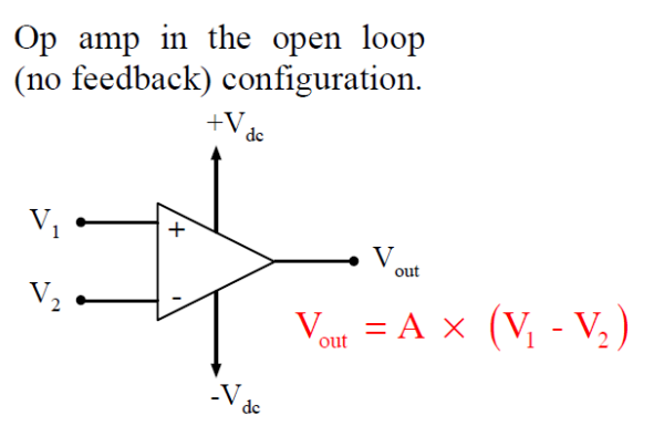
Op amp in the open loop (no feedback) configuration
Vout = A(V1 - V2)
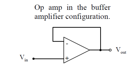
Op amp in the buffer amplifier configuration
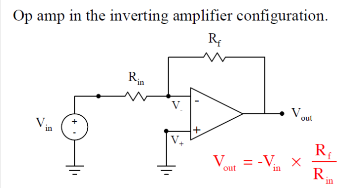
Op amp in the inverting amplifier configuration
Vout = -Vin(Rf/Rin)
An op amp’s output voltage is limited to be between _____
-Vdc < Vout < +Vdc
In amplitude modulation (AM), the amplitude of the carrier signal is modulated by _______
the signal being transmitted
In frequency modulation (FM), the frequency of the carrier signal is modulated by _______
the signal being transmitted
In your AM receiver circuit from Lab 8, the ______ rectified the signal, and the ______ removed the high frequency carrier wave.
diode, low pass filter
When converting an analog signal into a digital signal:
1) What is “sampling frequency”?
2) What is “bit depth”?
3) What is the Nyquist-Shannon sampling theorem?
1) sampling frequency is how often the amplitude of an analog signal is measured
2) Bit depth is the binary resolution (2n possible values) that the amplitude of an analog signal is measured
3) The Nyquist-Shannon sampling theorem guarantees that a signal can be reconstructed perfectly if the sampling rate is at least 2x the signal frequency
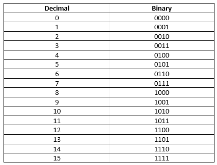
Be able to count up to 15 in binary
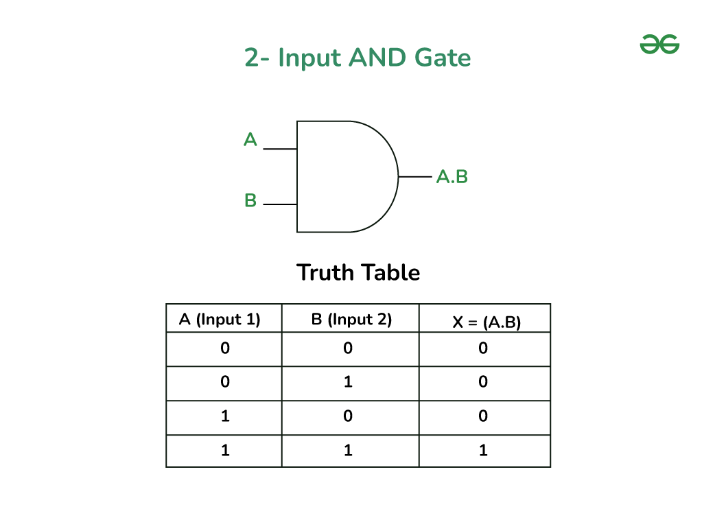
For an AND logic function/gate:
1) What is its truth table?
2) What is its circuit symbol?
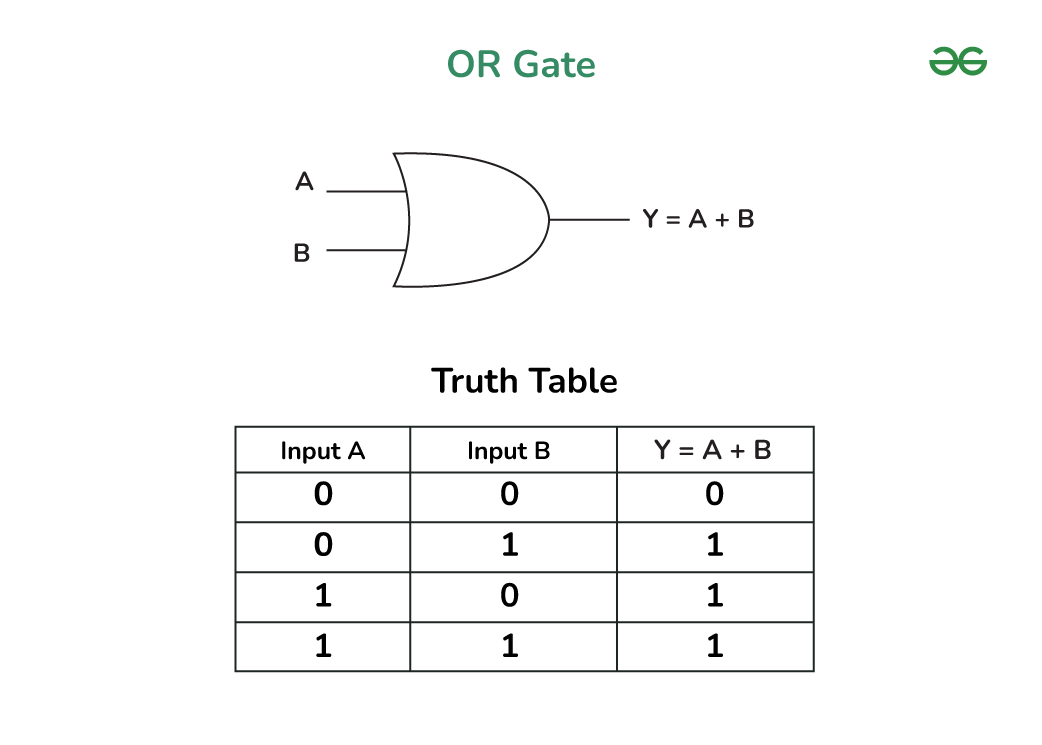
For an OR logic function/gate:
1) What is its truth table?
2) What is its circuit symbol?
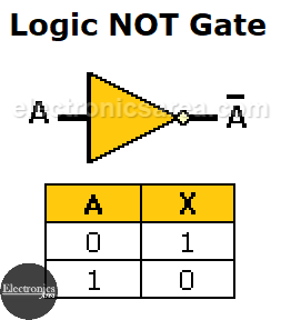
For an NOT logic function/gate:
1) What is its truth table?
2) What is its circuit symbol?
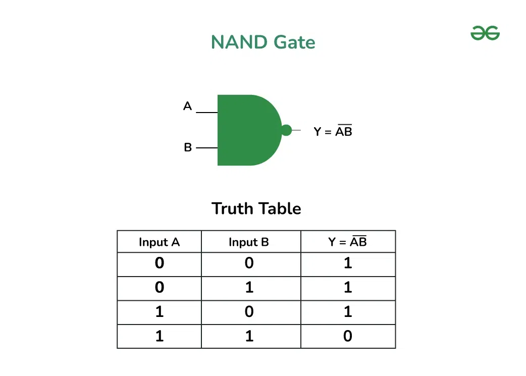
For an NAND logic function/gate:
1) What is the truth table?
2) What is its circuit symbol?
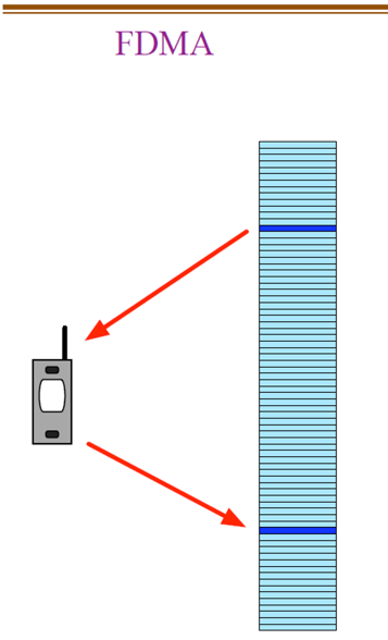
What does FDMA stand for, and how does it work?
FDMA stands for Frequency Division Multiple Access, a method of sending a cell phone signal over mobile communication networks.
How it works: each call is put on a separate frequency.
Simple Analogy: in a room of many people talking, you distinguish between different people by having each person talk at a different pitch.
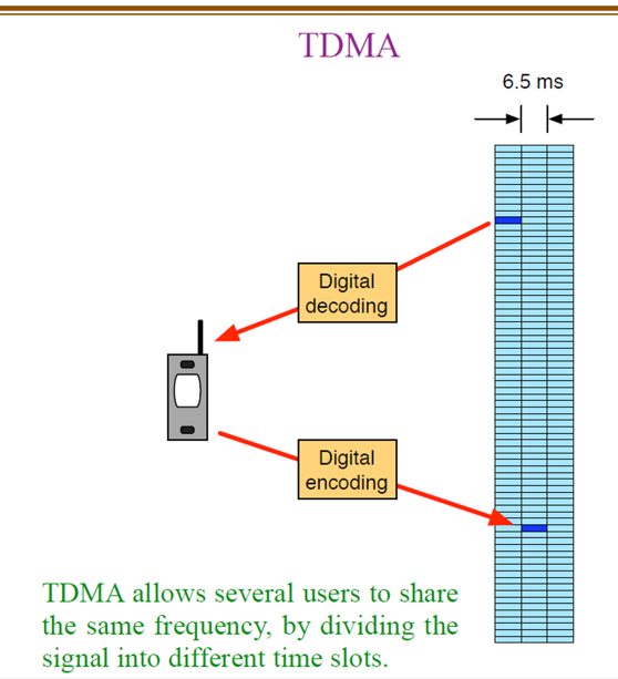
What does TDMA stand for, and how does it work?
TDMA stands for Time Division Multiple Access, a method of sending a cell phone signal over mobile communication networks.
How it works: each call is assigned a certain portion of time on a designated frequency.
Simple Analogy: in a room of many people talking, you distinguish between different people by having each person talk at a different time.
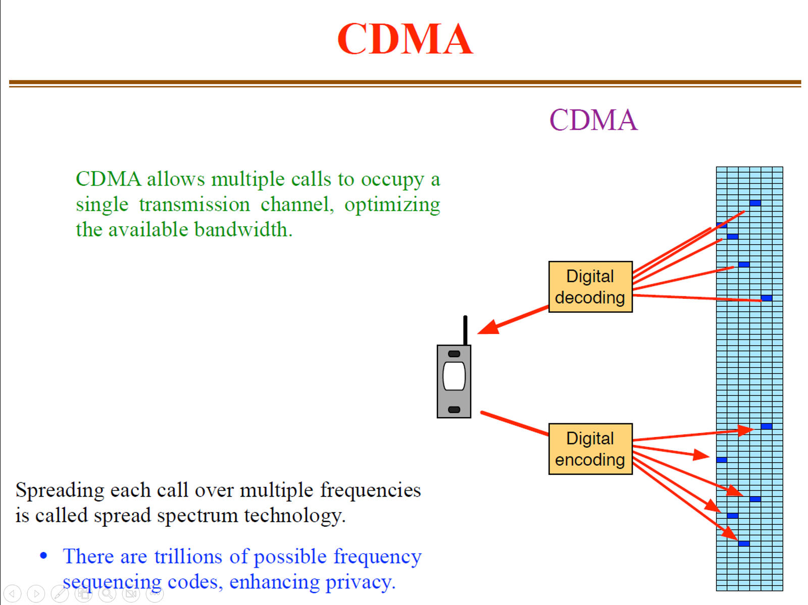
What does CDMA stand for, and how does it work?
CDMA stands for Code Division Multiple Access, a method of sending a cell phone signal over mobile communication networks.
How it works: each call (transmitter) is given a unique code, and the call is spread over all available frequencies.
Simple Analogy: in a room of many people talking, you distinguish between different people by having each person talk in a different language.
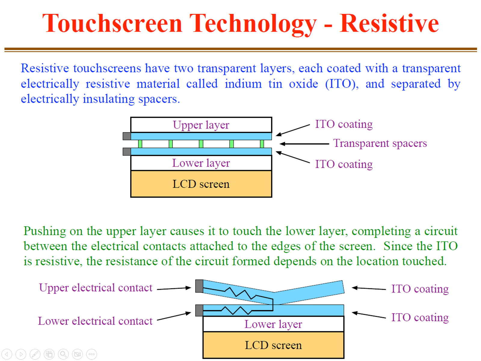
How do resistive touchscreens work?
Resistive touchscreens have 2 transparent layers coated with a transparent electrically resistive material called indium tin oxide (ITO), separated by electrically insulating spacers.
Pushing on the upper layer causes it to touch the lower layer and complete the circuit between the electrical contacts attached to the edges of the screen. Since the ITO is resistive, the resistance of the circuit formed depends on the location touched.
How do capacitive touchscreens work?
Capacitive touchscreens have arrays of wires and electrodes under the screen, which are made of transparent indium tin oxide (ITO). Electrical circuitry measures the capacitance between adjacent electrodes.
When capacitive touch screens are touched by objects that have a high dielectric constant (εr), the capacitance will change and the electronics detect touch. (Your fingers work because they have lots of water in them and the εr of water is ~80 at room temp).
You should understand the use of a “clock” in sequential logic circuits:
1) What is the use of a “clock” in sequential logic circuits?
2) Why is it important in synchronizing data movement?
3) Why are logic gates designed to only respond to the clock signal at the moment it switches from low to high (rising edge), or high to low (falling edge)?
1) In synchronous sequential circuits, the logic gates not only receive input from the logical variables, but also from a clock signal. The clock is used to prevent outputs from updating until all inputs have settled to desired new values, giving the circuit reliable output.
2) Logic gates take a finite amount of time to update their output when their inputs change. This can be a problem when many gates are interconnected. The clock is important to ensure the circuit will give reliable output.
3) Logic gates are often designed so that they only update at either the start (rising edge) or the end (falling edge) of a clock pulse because it ensures very precise updates.
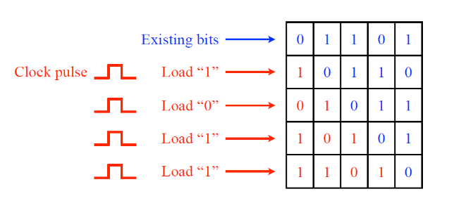
What is a shift register?
In a digital circuit, a “register” is a location where bits of information are stored.
In a shift register, information is transferred bit-by-bit across the register to make room for a new bit of information. Thus, at each cycle of the timing clock, all bits currently in the register shift over one place, and a new data bit is loaded into the vacated space.