Lec 3 | Process Flows | Lithography
1/16
There's no tags or description
Looks like no tags are added yet.
Name | Mastery | Learn | Test | Matching | Spaced | Call with Kai |
|---|
No analytics yet
Send a link to your students to track their progress
17 Terms
True or False: In a process of patterning gold thin film via lift off process, only negative photoresist can be used
False (can use positive or negative; one just needs to pay attention to how they want the pattern to show/develop)
True or False: In the photolithography process, illumination of the photoresist through the mask directly results in the formation of the patterned film
False (need developing solution to form the pattern; shining light makes the photoresist insoluble or soluble and then needs developing solution)
What is the primary role of Novac in the photoresist?
a) Photoacid generator
b) Photoactive compound
c) Improves resistance towards subsequent etching
d) chemical amplifier
c) Improves resistance towards subsequent etching
True/False: A smaller Airy disk is needed so that smaller patterns can be defined
True (can bring them closer together if smaller radius)
A bigger airy disk can be obtained by…
a) Using a bigger lens
b) Using larger wavelength
b) Using larger wavelength (larger wavelength → larger airy disk; additionally, using a bigger lens means more of the diffracted light can be captured, which creates a smaller airy disk)
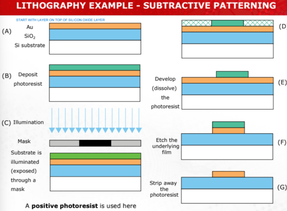
DRAW | Identify the key characteristics and process flow: subtractive patterning
METAL ALR ON TOP
1) Start with metal layer (Au) on top of the SiO2 layer
2) Deposit Photoresist
3) Substrate is illuminated (exposed) through a mask
4) Develop (dissolve) the photoresist
5) Etch the underlying film (etch the Au)
6) STRIP AWAY THE PHOTORESIST | DONE
SILICON DIOXIDE LAYER IS STILL INTACT
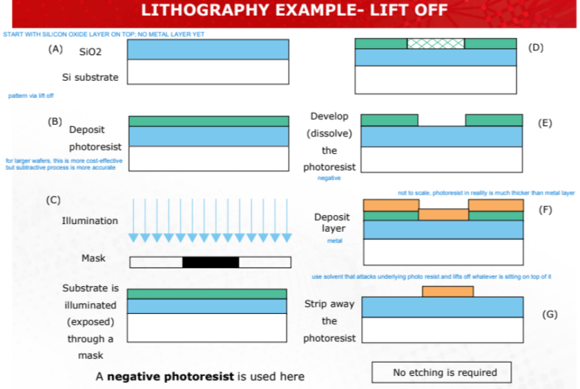
DRAW | Identify the key characteristics and process flow: Lift-off
1) Start with SiO2 layer on top (no metal yet)
2) Deposit photoresist
3) Illuminate substrate through mask
4) Develop (dissolve) the photoresist
5) DEPOSIT (METAL) LAYER (photoresist is typically much thicker than metal layer)
6) Strip away the photoresist (use solvent that attacks underlying photoresist and lifts off whatever is sitting on top of it) | DONE
NO ETCHING IS REQUIRED
SILICON DIOXIDE LAYER IS STILL INTACT
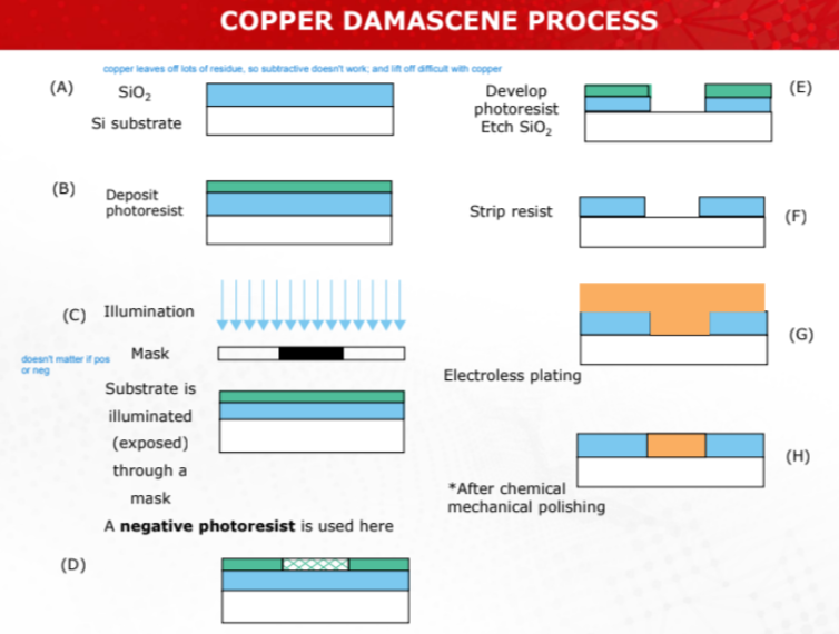
DRAW | Identify the key characteristics and process flow: Copper Damascene
1) Start with SiO2 on top of Si substrate
2) Deposit photoresist
3) Illumination through mask
4) Develop photoresist, Etch SiO2
5) Strip resist
6) Electroless plating (FILL TRENCHES TO FORM CONDUCTIVE COPPER INTERCONNECTS)
7) POLISH - metal flush with SiO2 layer | DONE
Compare the different methods of patterning wafers: Copper Damascene vs. Lift-Off vs. Subtractive patterning
Copper Damascene: Ideal for copper interconnects; leaves residues due to electroplating overburden and CMP; high precision but costly; not suited for non-metal materials.
Lift-Off: Simple and cost-effective; suitable for non-etchable materials; struggles with copper due to poor adhesion, non-directional deposition, and high melting point; limited scalability.
Subtractive Patterning: High precision and scalability; versatile for metals and dielectrics but unsuitable for copper due to difficult etching and potential substrate damage.
Residue and Accuracy: Copper Damascene leaves residues; Subtractive offers highest accuracy; Lift-Off has lower precision.
Cost and Use Cases: Lift-Off is cheapest for prototyping; Subtractive suits high-resolution needs; Damascene excels in copper-dependent applications.
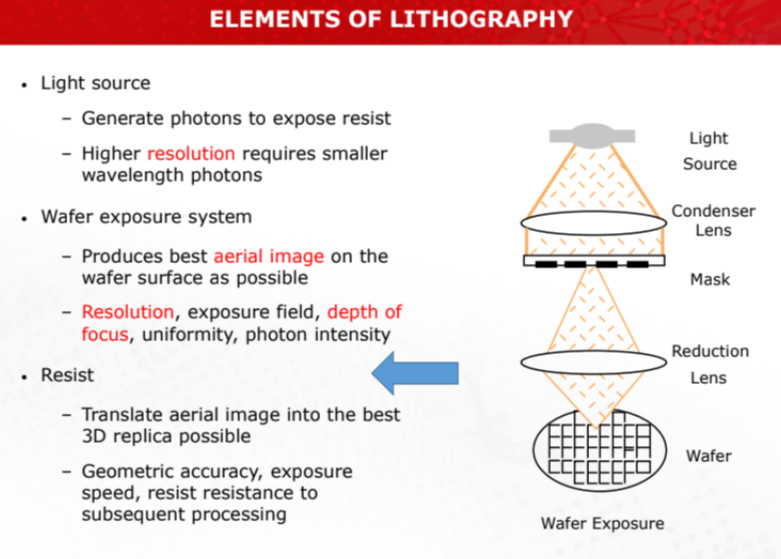
Explain the basic principles of Lithography
Light Source
generate photons to expose resist (smaller wavelength photons → higher resolution - smaller feature size)
STEPS
Photoresist
Project light through mask
Developing solution
LEADS TO PATTERN
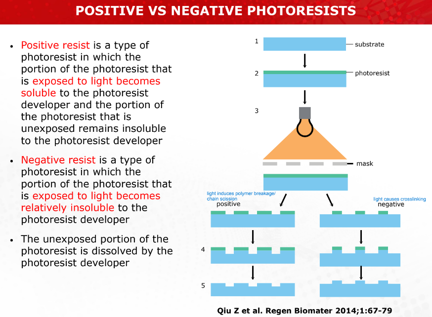
Differentiate between positive and negative photoresistors
Positive Photoresists | POSITIVE IMAGE OF MASK
Exposure Effect: Becomes soluble in the developer solution when exposed to light (exposed areas are removed).
Resolution: Generally provides higher resolution due to sharper edges of the developed pattern.
Usage: Preferred for applications requiring fine feature patterning (e.g., IC manufacturing).
Chemical Composition: Contains photosensitive compounds that degrade upon light exposure.
Negative Photoresists | NEGATIVE IMG OF MASK
Exposure Effect: Becomes insoluble (crosslinks/polymerizes) in the developer solution when exposed to light (unexposed areas are removed).
Resolution: Typically lower resolution due to swelling and merging of exposed areas.
Usage: Used for less demanding applications or thicker film requirements (e.g., MEMS fabrication).
Chemical Composition: Contains photoinitiators that cause polymerization upon light exposure, cross-linking the resist.
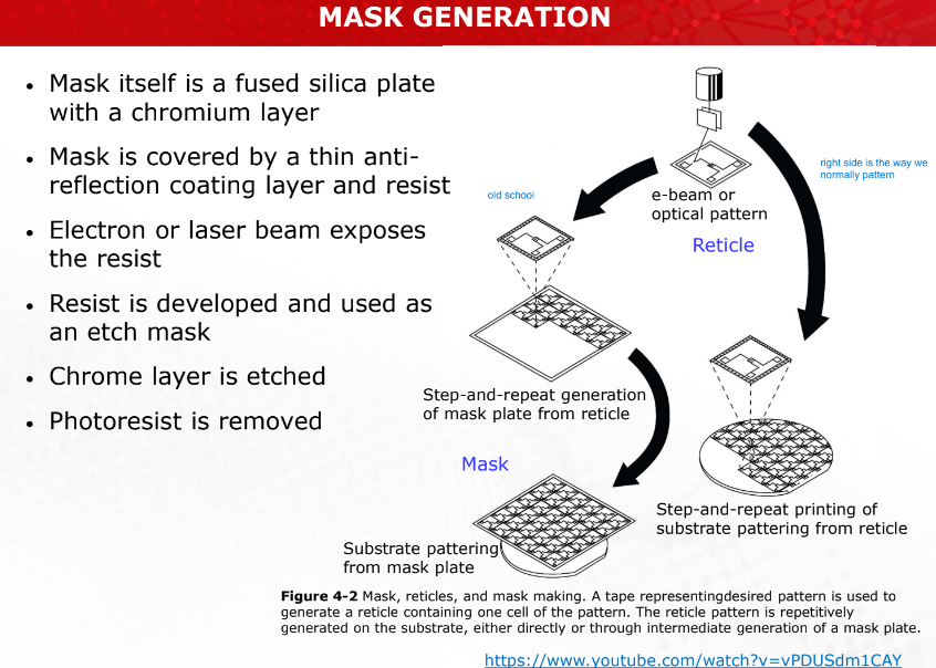
Explain the process of mask fabrication
made fused silica plate with Cr layer
covered with anti-reflection coating AND RESIST
electron or laser beam exposes the resist
resist developed and used as etch mask
chrome layer etched
photoresist removed
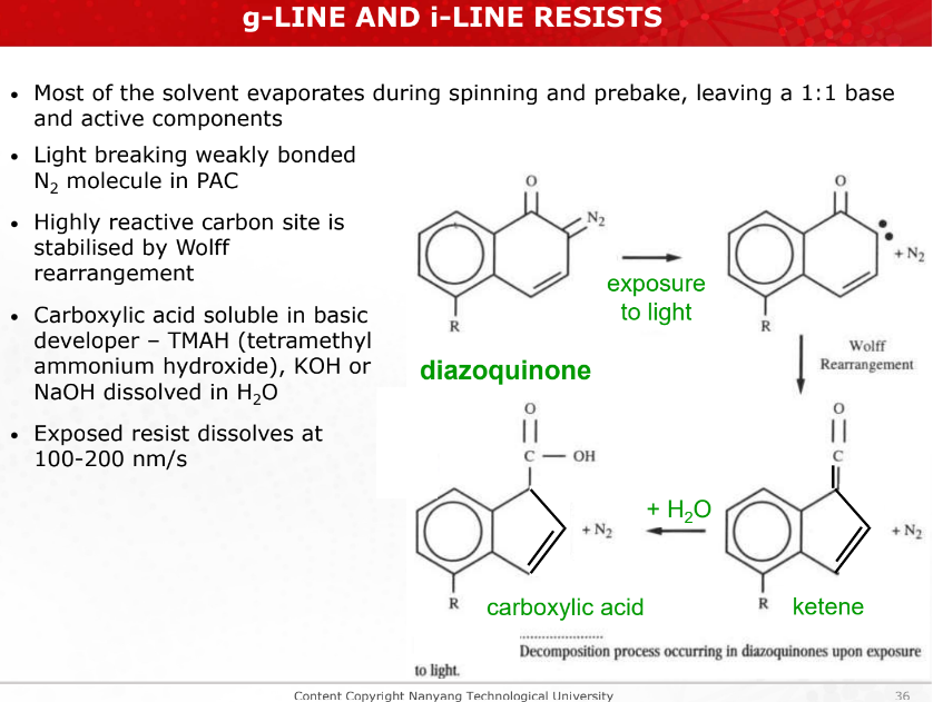
What are the components of g-line and i-line photoresists, and how do they function?
Hg arc lamps: g-line = 436 nm exposure wavelength i-line = 365 nm
g-line and i-line photoresists consist of:
Novolac resin: Dissolves readily in the developer.
Photoactive compound (PAC): Diazonaphthoquinones (DNQ) inhibit dissolution until exposed to light.
Solvent: Adjusts viscosity.
When exposed to light, diazonaphthoquinones (DNQ) decompose to form carboxylic acids, making the exposed areas soluble in a basic developer.
Why are smaller wavelength light sources preferred in lithography?
Smaller wavelength light sources, such as Hg arc lamps (g-line at 436 nm, i-line at 365 nm) and excimer lasers (KrF at 248 nm, ArF at 193 nm), allow Advantages and Disadvantages of g-line and i-line Resists. They enable the creation of finer patterns essential for modern microelectronics.
Advantages and Disadvantages of g-line and i-line Resists
Advantages: Exposed regions unaffected by developer → High resolution img of mask, and good etch resistance (Novolac resist).
Disadvantages: Below 365 nm (i-line), resists strongly absorb incident photons → incident radiation cannot penetrate through full thickness of resist limiting light penetration AND Low intensity of Hg lamps at shorter wavelengths reduces efficiency.
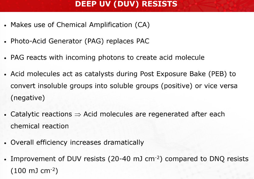
What distinguishes DUV photoresists from g-line and i-line resists?
DUV resists use a Photo-Acid Generator (PAG) instead of PAC. Upon exposure to deep ultraviolet light, PAG generates acid molecules that catalyze chemical reactions during Post Exposure Bake (PEB), increasing the efficiency and resolution compared to DNQ resists.
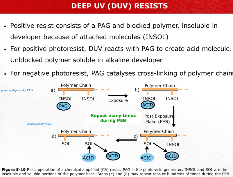
Advantages and Challenges of DUV Resists
Benefits: Excellent sensitivity and resolution due to chemical amplification, requiring lower light doses (20-40 mJ/cm²).
Challenges: Acid-molecule contamination and diffusion between exposure and PEB can degrade accuracy (i.e. acid molecules may diffuse into even the unexposed parts of the photoresist). Strict control of PEB conditions is necessary.