EEE 120 Quiz 1 Electrical Fundamentals and Logic Gates
1/18
There's no tags or description
Looks like no tags are added yet.
Name | Mastery | Learn | Test | Matching | Spaced | Call with Kai |
|---|
No analytics yet
Send a link to your students to track their progress
19 Terms
Most digital circuits represent binary values using ________. _______
0 V and +5 V
LOW (or binary 0) in a digital system typically corresponds to ________.
0 V
The rising edge of a digital clock occurs when
the signal changes from LOW to HIGH
What is the frequency of a clock waveform whose period is 20 microseconds
50 kHz
The Boolean equation for an OR gate is ________.
A + B = X
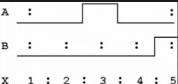
Waveforms A and B represent the inputs to an AND gate. During which time interval will the output from the gate (X) be HIGH?
time interval 2
If both inputs of an AND gate are normally HIGH but one of them momentarily dips LOW, the output will
momentarily dip LOW
The Boolean equation for a NAND function is
X = (AB)’
Which logic function can be implemented by connecting an inverter to the output of an OR gate?
NOR
Which logic function can be implemented by connecting an inverter to the output of a NAND gate?
AND
Can you construct an XOR gate using only AND/OR/NOT gate(s)?
Yes
Which gate can be used to generate a true output if an odd number of inputs is true?
XOR
An NAND gate with inverters connected to each input behaves like OR gate
True
What is the period of a clock waveform whose frequency is 4 mHz?
250 s
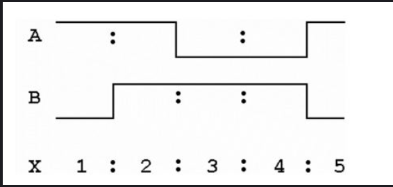
Waveforms A and B represent the inputs to an OR gate. During which time interval(s) will the output from the gate (X) be HIGH?
time intervals 3 and 5
Which logic function is represented by the equation ABCD = X?
AND
If one input of an AND gate is HGH while the other is a clock signal, the output is
a clock signal
If one input of an OR gate is HIGH while the other is a clock signal, the output is
HIGH
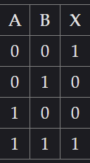
Which logic gate is described by the following truth table?
XNOR