Electronic Circuit Design 2 - Week 9 - Asynchronous DAC concepts
1/30
There's no tags or description
Looks like no tags are added yet.
Name | Mastery | Learn | Test | Matching | Spaced | Call with Kai |
|---|
No analytics yet
Send a link to your students to track their progress
31 Terms
what does VFSR stand for
the voltage Full scale range
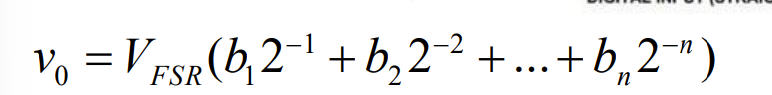
for the Ideal DAC Transfer function what is the main equation you need to remember to calculate the voltage output
draw the ideal DAC transfer function circuit
does b1 refer to the highest or lowest bit in a digital number
it refers to the MSB not the LSB
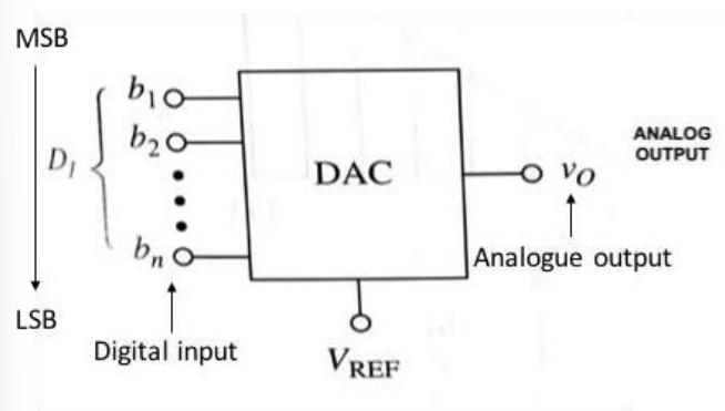
what is the function of a DAC in words
it accepts an n bit input word and produces an analogue output
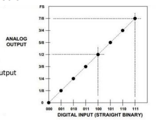
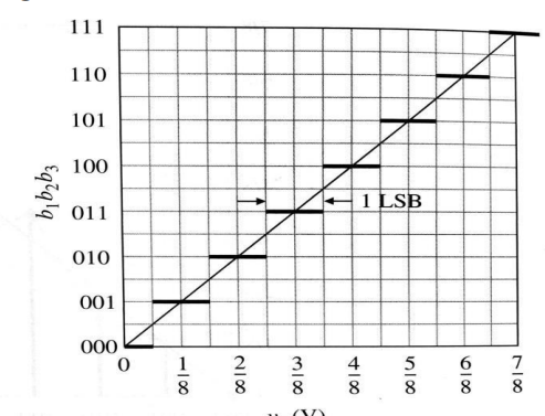
draw the envelope graph for a DAC showing analogue output and digital input if it is a 3 bit word with the VFSR =1
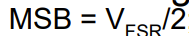
what is the equation for a DAC to calculate the MSB
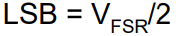
what is the eqaution for calculating the LSB
note it is the same as the resolution
what is the equation for calculating the resolution of a DAC
note it is the same as the LSB

what is the equation you need to remember for caluculating the dymanic range of a DAC in DB
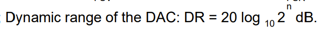
what is the dynamic range of a 12 bit DAC

what is the function of an ADC in words
it accepts an analogue input signal and produces a digital code
For an ADC draw the enevelope graph for a 3 bit word with the VREF between 0 and 1. comment on the values.
A certain range of analogue signals produces the same digital code as the midrange value. the range is the midrange value +or - ½ the LSB.
for a 3 bit ADC with the VFSR = 1 draw the envelope of the quantization error also called eq. what shape does it take
a sawtooth wabe
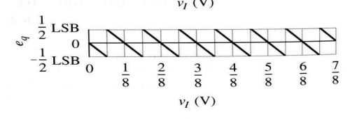
what does eq stand for in an ADC
quantization error
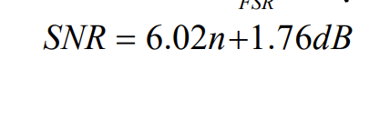
what is the equation for SNR you need to rememebr
For the weighted resistor DAC draw a 4 bit version of it
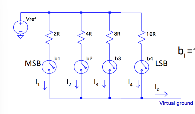
For the weighted resistor DAC derive the output current and the Voltage output
check notes labelled weighted resistor DAC
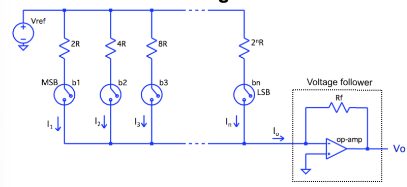
what is the weighted resistor DAC usually connected to draw the diagram
it is usually connected to a voltage follower
statge the advantges o the weighted reisisot DAC
it is connecptually simple you just connecte a voltgae follower to the ouput of a DAC.
only N reisistors and switches required
statge the disadvantges o the weighted reisisot DAC
resistance spread exponentially increasing with N. so as N gets large you need very high value resistors and it is hard to ensure accurate ratios between the resistors.
the effect of switch resistance can be wquite alot it is most important for the MSB as this uses the largest reistor so has a bigger effect.
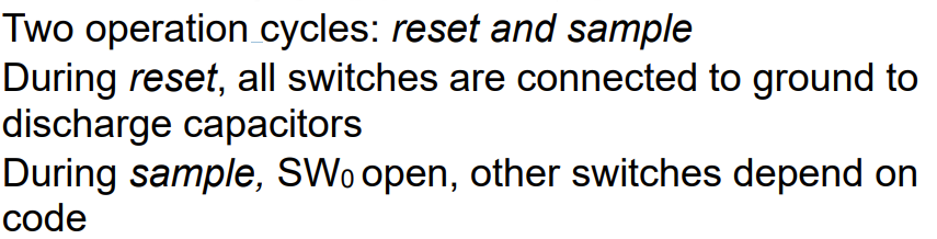
what are the two modes of operation for a weighted capacitor DAC and explain them
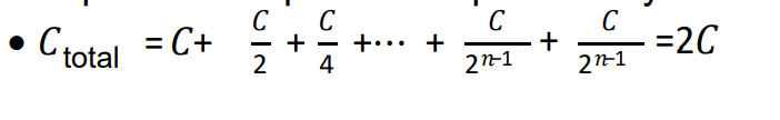
write down the formula which explains the capacitance spread for the weighted capacitor DAC
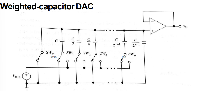
draw the schematic for the weighted capacitor DAC
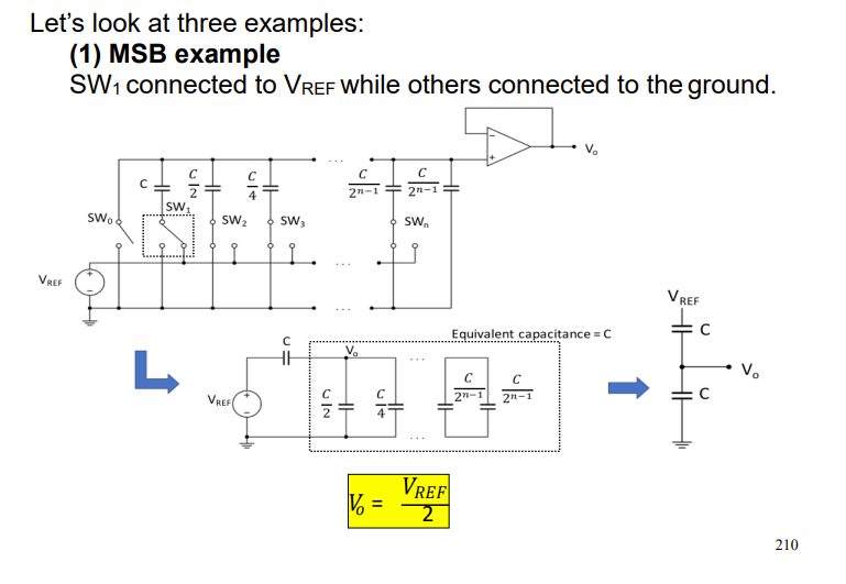
for the weighted capacitor DAC derive the ouput voltage when only the MSB is connected to VREF. case 1.
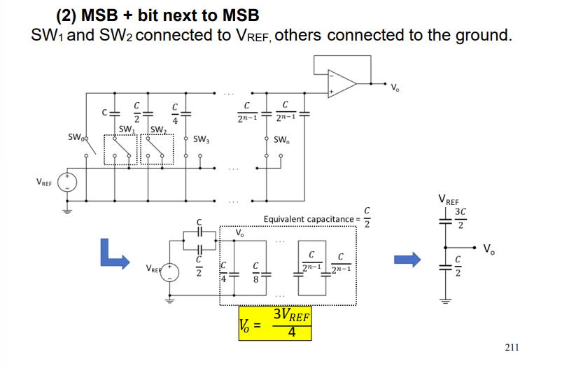
for the weighted capacitor DAC derive the ouput voltage when the MSB is connected to VREF and the next bit is but nothing else . case 2.
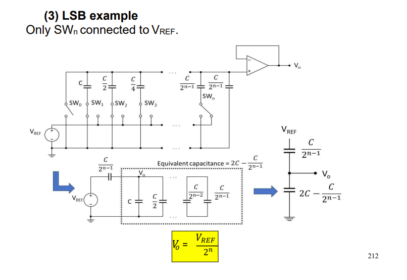
for the weighted capacitor DAC derive the ouput voltage when the LSB is connected to VREF only . case 3.
check notes. for all cases.
what is the overall transfer function for the weighted capacitor DAC.

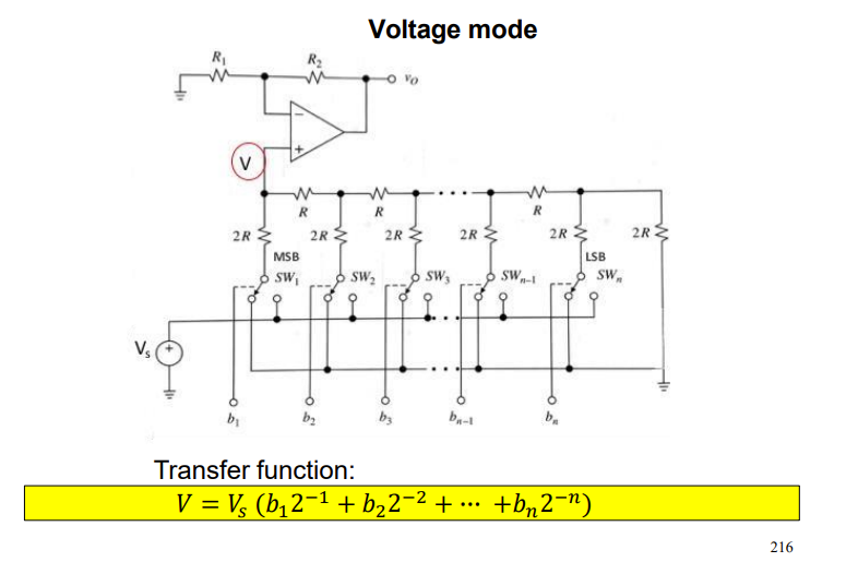
what are the 3 important properties of a R2R ladder DAC
from right to left equivalent resistance of each labelled node is always 2R
voltages are weighted where as bit number goes from MSB to LSB the voltage halves
currents are weighted where as bit number goes from MSB to LSB the current halves
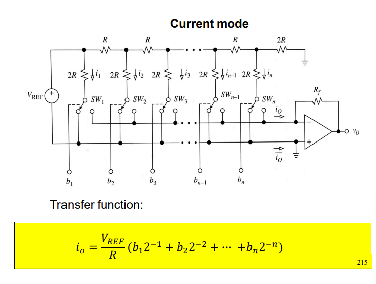
draw the R2R DAC Ladder in current mode and state equaiton
draw the R2R DAC Ladder in voltage mode and state equaiton