Chapter 1: Semiconductor Diodes
1/60
There's no tags or description
Looks like no tags are added yet.
Name | Mastery | Learn | Test | Matching | Spaced | Call with Kai |
|---|
No study sessions yet.
61 Terms
Jack Kilby (1923-2005)
Created the first integrated circuit at Texas Instruments in 1958, using a single piece of semiconductor. He had countless awards and honors including a Nobel Prize in Physics in 2000.
Dr. Gordon E. Moore
- Co-founder of Intel Corporation and author of Moores Law
- In 1965, he presented a paper predicting that the transistor count in a single IC chip would double every two year.
Diode (1939)
A device that permits current to flow through it in only one direction.
Semiconductors
are a special class of elements having a conductivity between that of a good conductor and that of an insulator.
Single-Crystal and Compound
Semiconductor materials fall into one of two classes.
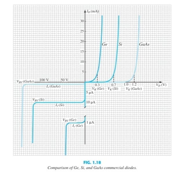
Ge, Si, and GaAs.
There are the three semiconductors used most frequently in the construction of electronic devices.
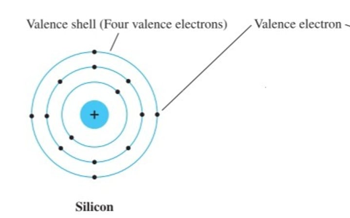
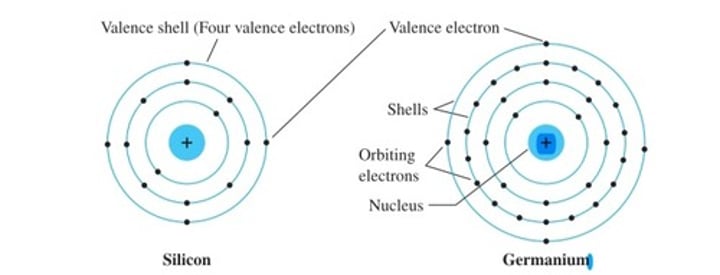
Silicon (Si)
- It is still the fundamental building block for Intel's new line of processors.
- In 1954 the first silicon transistor was introduced, and it quickly became the semiconductor material of choice.
- Not only is it less temperature sensitive, but it is one of the most abundant materials on earth.
Gallium Arsenide (GaAs)
- A crystalline, high-efficiency compound used to make certain types of solar cells and semiconductor material.
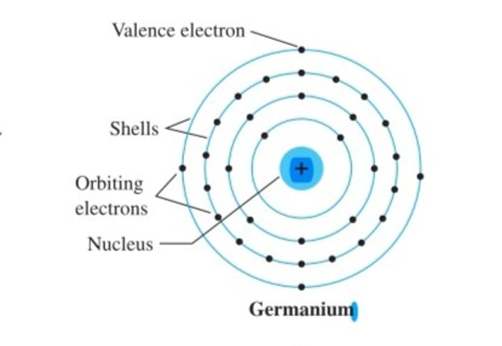
Germanium (Ge)
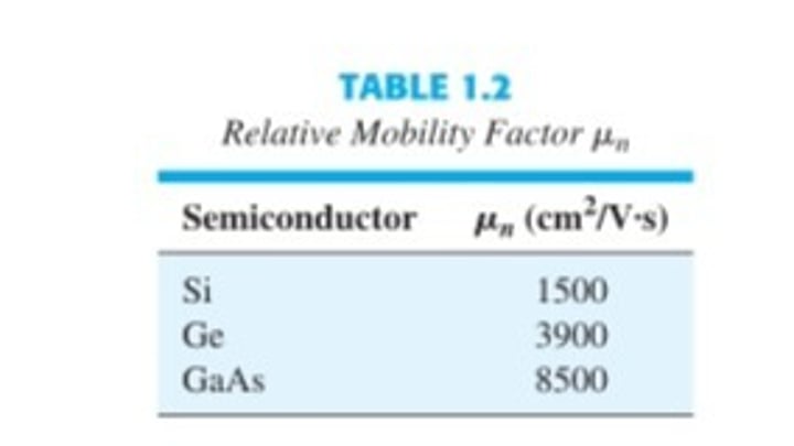
It is in limited production due to its temperature sensitivity and high reverse saturation current. It is still commercially available but is limited to some high-speed applications (due to a relatively high mobility factor) and applications that use its sensitivity to light and heat such as photodetectors and security systems.
Tetravalent
Atoms that have four valence electrons.
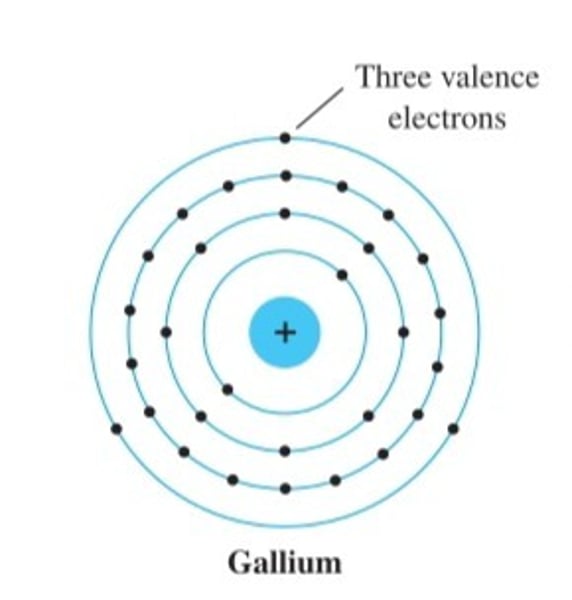
Trivalent
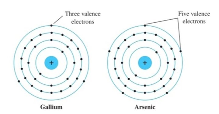
Atoms that have three valence electrons.
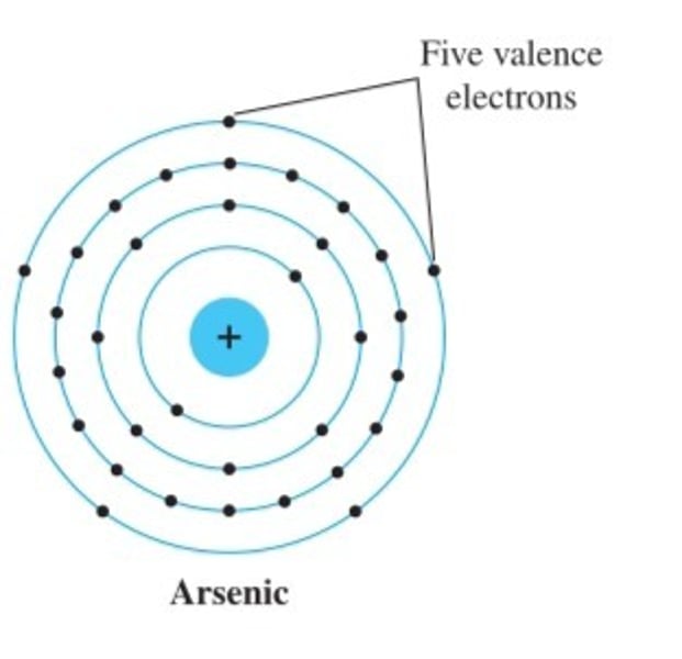
Pentavalent
Atoms that have five valence electrons.
Covalent Bonding
A bond formed when atoms share one or more pairs of electrons.
Intrinsic Materials
These are those semiconductors that have a very low level of impurities.
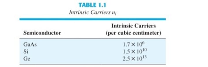
Intrinsic Carriers
The free electrons in a material due only to external causes are referred to as
Extrinsic Material.
A semiconductor material that has been subjected to the doping process.
Free
This term is applied to any electron that has separated from the fixed lattice structure and is very sensitive to any applied electric fields such as established by voltage sources or any difference in potential
Free Carriers
The ability of the free carriers to move throughout the material.
Doping Semiconductors
The addition of an impurity element to a semiconductor.
The farther an electron is from the nucleus
The higher is the energy state, and any electron that has left its parent atom has a higher energy state than any electron in the atomic structure.
N-type and P-type Materials
Two extrinsic materials of immeasureable importance to semiconductor device fabrication.
An N-type Material
- Created by introducing impurity elements that have five valence electrons ( pentavalent ), such as antimony , arsenic , and phosphorus.
-The electron is called the majority carrier and the hole the minority carrier.
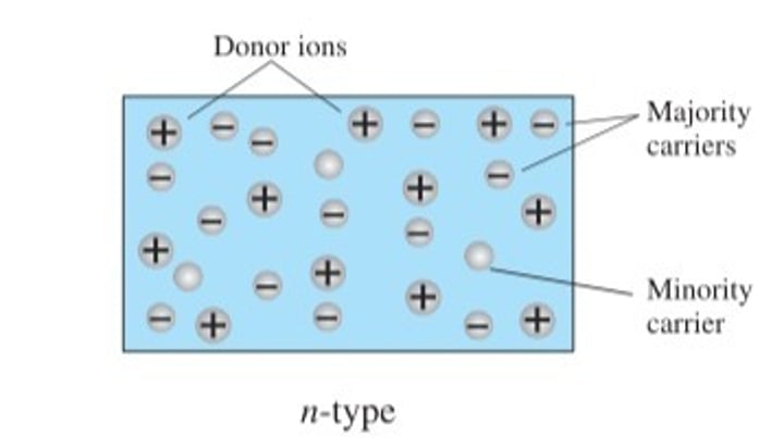
Donor Atoms
Diffused impurities with five valence electrons.
A P-type Material
- Formed by doping a pure germanium or silicon crystal with impurity atoms having three valence electrons. The elements most frequently used for this purpose are boron, gallium, and indium.
- The hole is the majority carrier and the electron is the minority carrier.
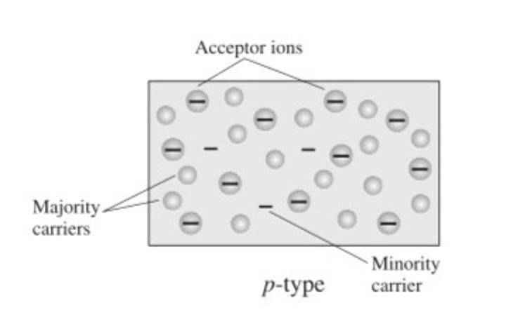
Holes
This results vacancy and is represented by a small circle or a plus sign, indicating the absence of a negative charge.
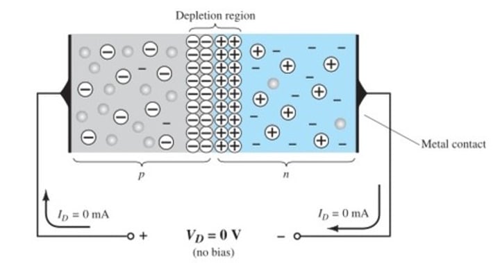
The Semiconductor Diode
It is created by simply joining an n -type and a p -type material together.
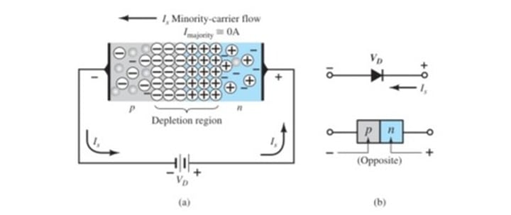
Depletion Region
This region of uncovered positive and negative ions.
Bias
This term refers to the application of an external voltage across the two terminals of the device to extract a response.
Zero
- In the absence of an applied bias across a semiconductor diode, the net flow of charge in one direction and the current under no-bias conditions is
- This widening of the depletion region will establish too great a barrier for the majority carriers to overcome, effectively reducing the majority carrier flow to
Reverse Saturation Current
The current that exists under reverse-bias conditions.
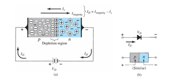
Forward-Biased
It is established by applying the positive potential to the p -type material and the negative potential to the n -type.
Breakdown Potential
The reverse-bias potential that results in this dramatic change in characteristic.
An Ionization Process
It will result whereby valence electrons absorb sufficient energy to leave the parent atom. These additional carriers can then aid the ionization process to the point where a high avalanche current is established and the avalanche breakdown region determined.
Zener Breakdown
It will contribute to the sharp change in the characteristic. It occurs because there is a strong electric field in the region of the junction that can disrupt the bonding forces within the atom and "generate" carriers.
Zener region
The sharp change in the characteristic at any level.
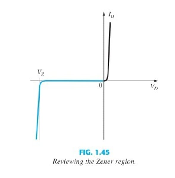
Zener Diodes
Diodes employing this unique portion of the characteristic of a p - n junction.
Peak Inverse Voltage (PIV rating) / Peak Reverse Voltage (PRV rating)
The maximum reverse-bias potential that can be applied before entering the breakdown region.
Temperature
It can have a marked effect on the characteristics of a semiconductor diode.
Operating Speed
An important factor in today's market.
Higher Mobility
Research today is also looking at compounds in groups III-V that have these factors to ensure that industry can meet the demands of future high-speed requirements.
Reverse-Biased
A p - n junction will permit a very small level of current to flow.
Reverse Breakdown Voltage
A semiconductor diode will increase or decrease with temperature.
February 23, 1940
Ohl found that a silicon crystal with a crack down the middle would produce a significant rise in current when placed near a source of light.
Body Resistance
All the resistance levels determined thus far have been defined by the p - n junction and do not include the resistance of the semiconductor material itself.
Contact Resistance
The resistance introduced by the connection between the semiconductor material and the external metallic conductor.
Frequency Sensitive
Every electronic or electrical device is
Transition Capacitance
It is the predominant capacitive effect in the reverse-bias region.
Diffusion Capacitance
It is the predominant capacitive effect in the forward-bias region.
Rectifier
This term is applied to a diode when it is frequently used in a rectification process.
Rectification
The process by which alternating current is changed to pulsating direct current.
Light-Emitting Diode
It is a diode that gives off visible or invisible (infrared) light when energized.
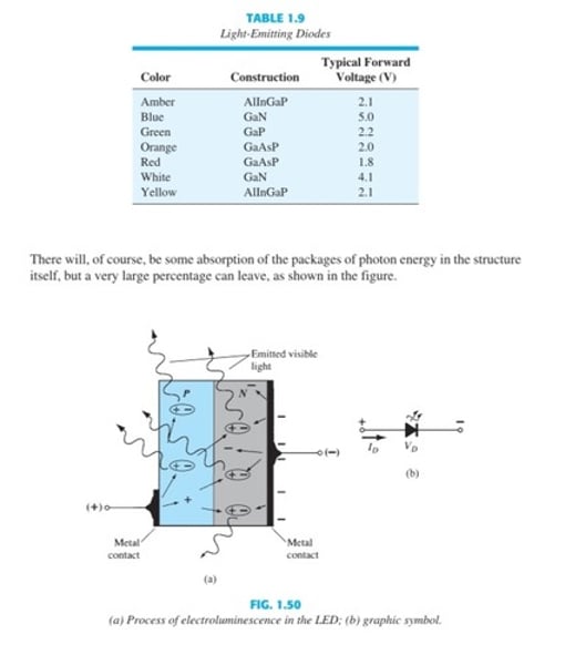
Invisble Light
It has a lower frequency spectrum than visible light.
Normalized
This term is used frequently on graphs to give comparisons of response to a particular level.
A Normalized Plot
It is one where the variable of interest is plotted with a specific level defined as the reference value with a magnitude of one.
The Light Intensity
An LED will increase with forward current until a point of saturation arrives where any further increase in current will not effectively increase the level of illumination.
Efficacy
This term is, by definition, a measure of the ability of a device to. For the LED this is the ratio of the number of lumens aware of the next chapter one protective.
Ideal Diode
It is a short in the region of conduction and an open circuit in the region of nonconduction.
Increasing Temperatures
It can cause a significant increase in the number of free electron in a semiconductor material.
0.7 V
The threshold voltage for silicon diodes.
0.3 V
The threshold voltage for germanium diodes.
Russell Ohl (1898 - 1987)
Determined to demonstrate that the future of the field was defined by semiconductor crystal.