defects
 Call Kai
 Learn
Learn Practice Test
 Spaced Repetition
 Match
Match Flashcards
 Knowt Play
1/32

There's no tags or description
Looks like no tags are added yet.
Name | Mastery | Learn | Test | Matching | Spaced | Call with Kai | Chat |
|---|
No analytics yet
Send a link to your students to track their progress
33 Terms
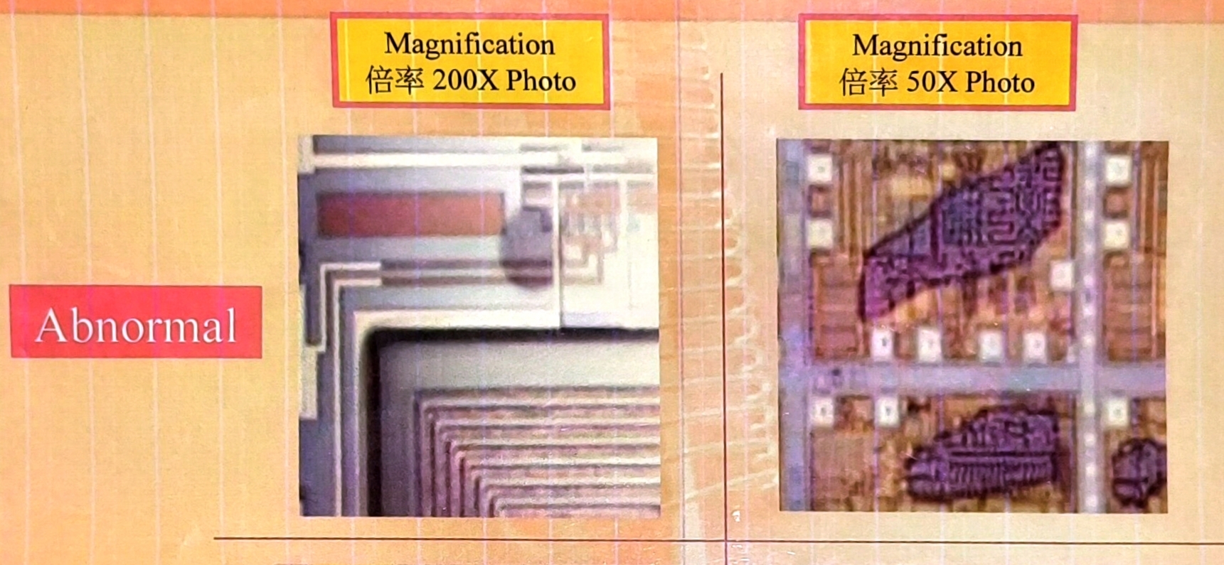
.
Ink Residue
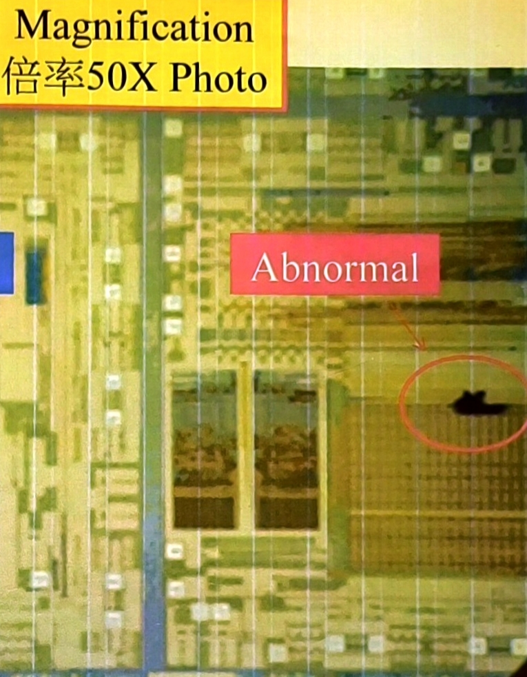
.
Ink Lose
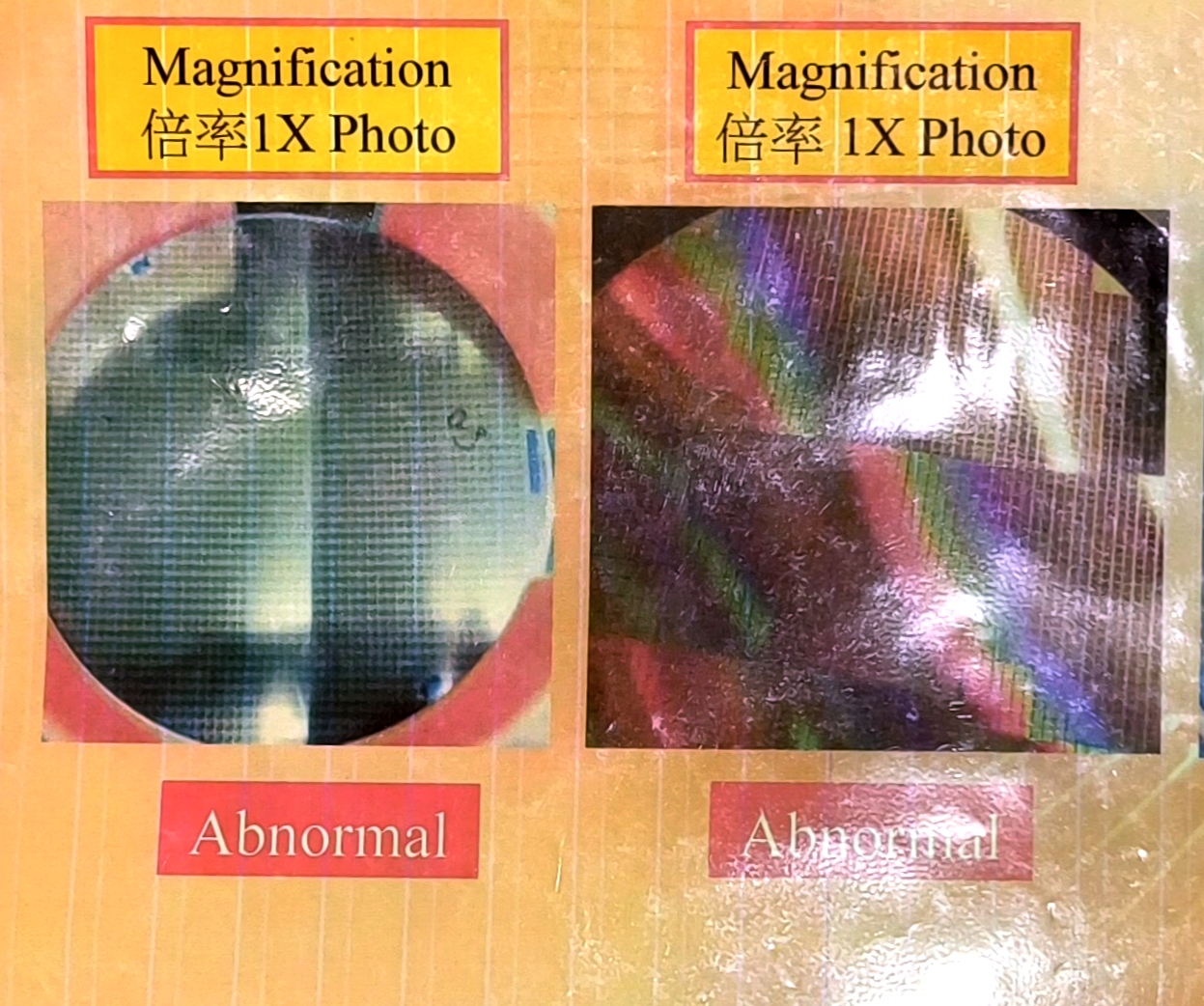
.
Wafer Broken
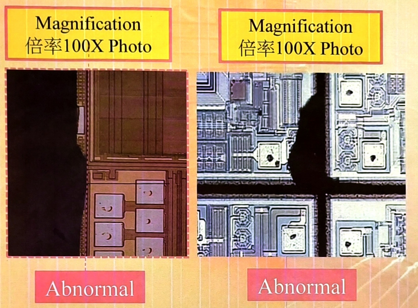
.
Die Chip/Crack
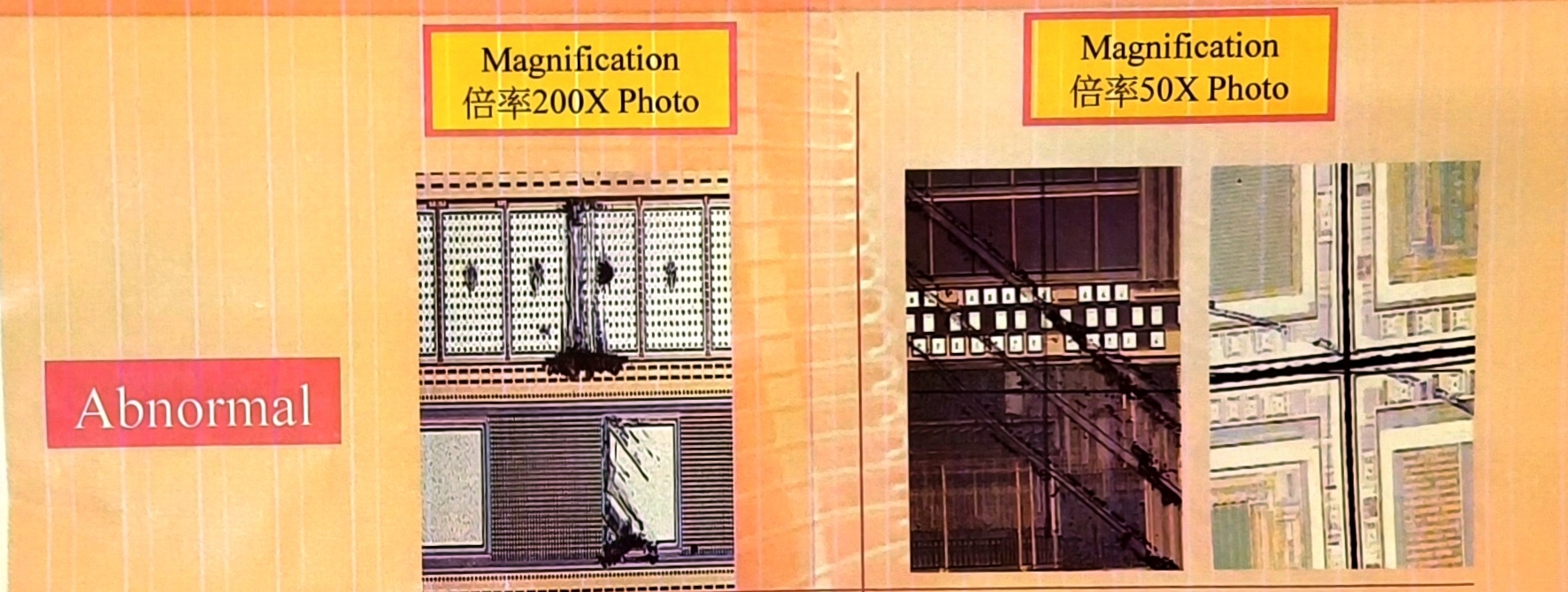
.
Surface Scratch
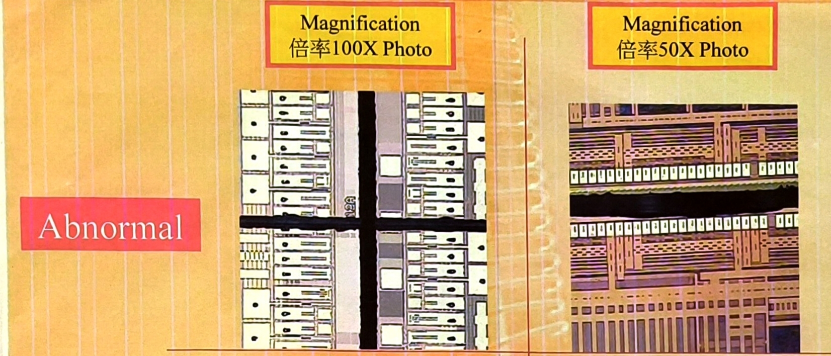
.
Kerf Mis-placement
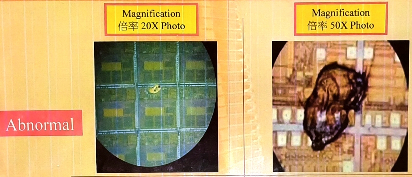
.
Wafer Foreign Matter
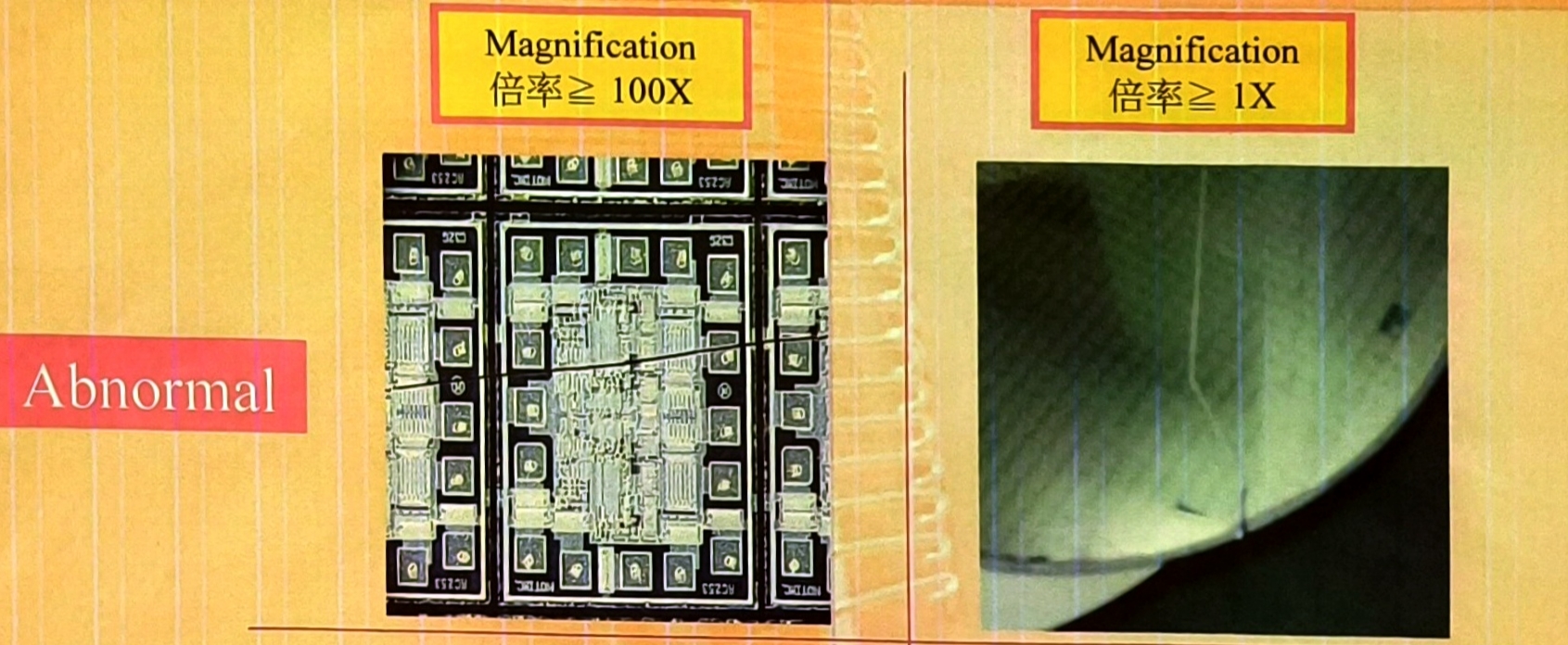
.
Wafer Broken
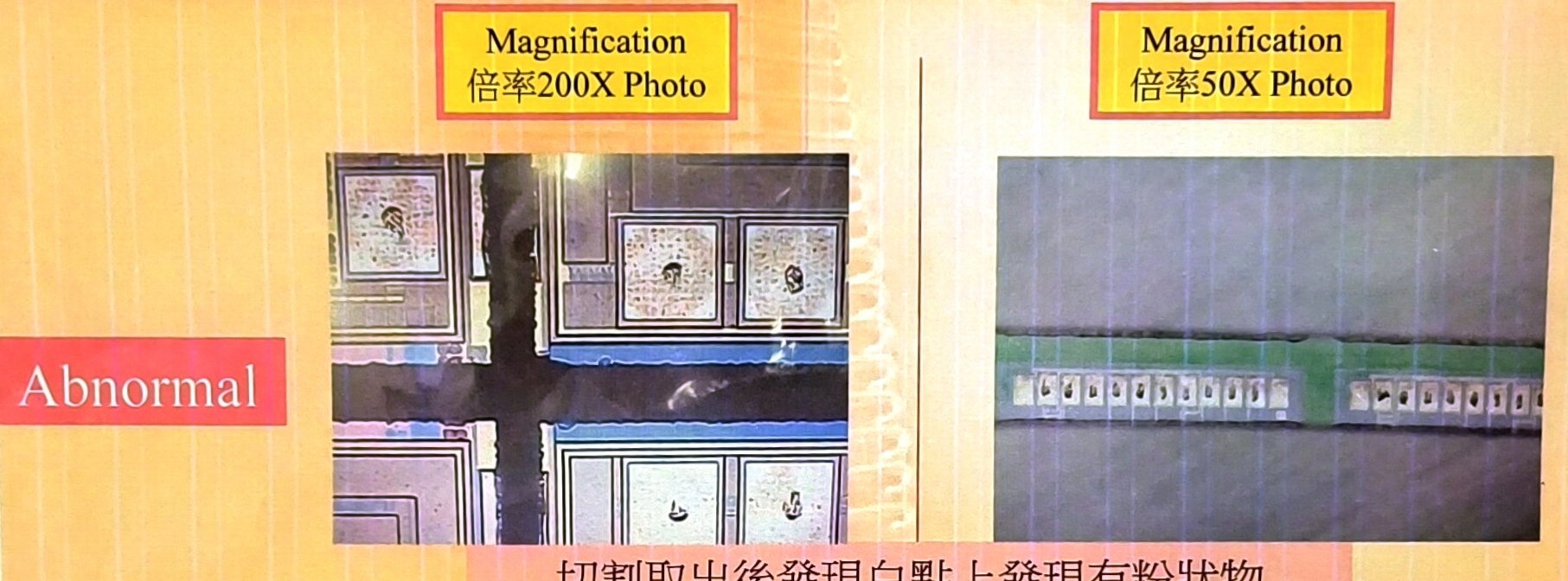
.
Silicon Dust
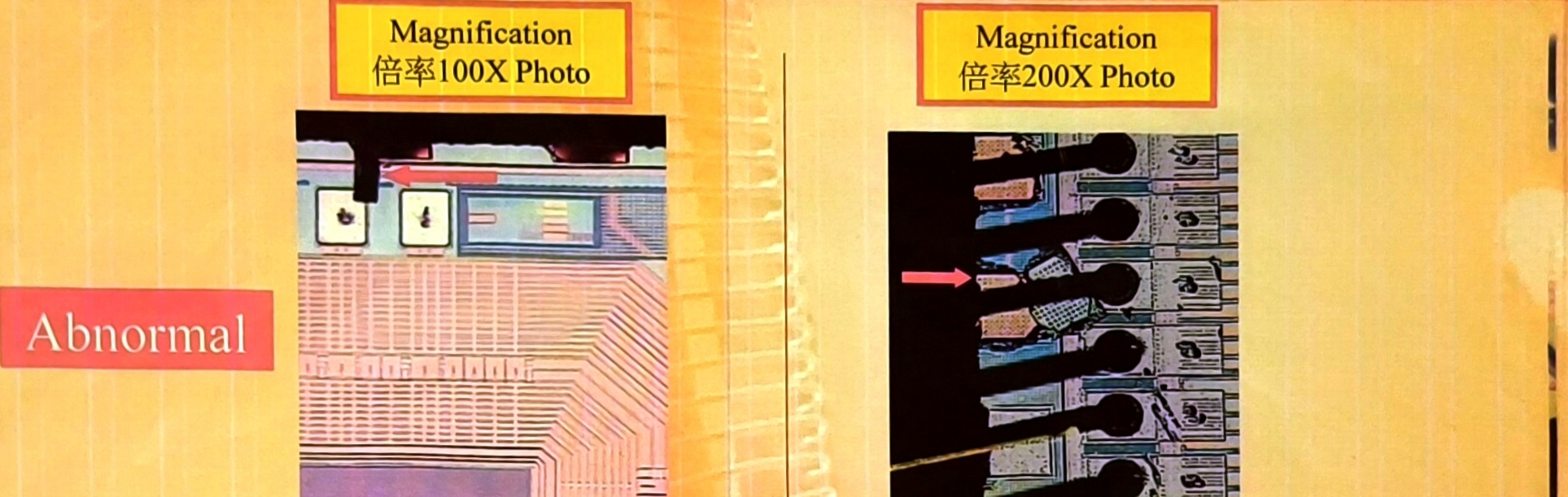
.
Peeling
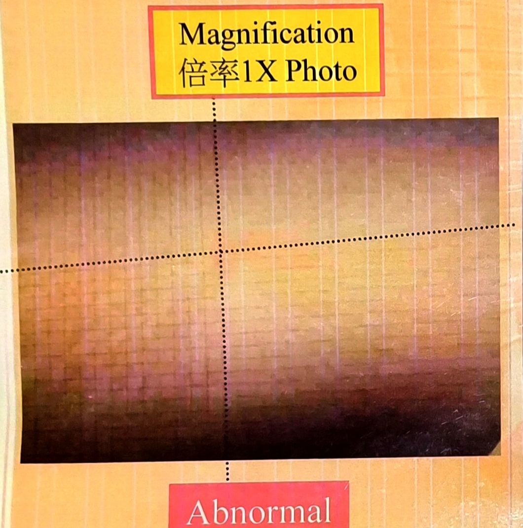
.
Incomplete Cut
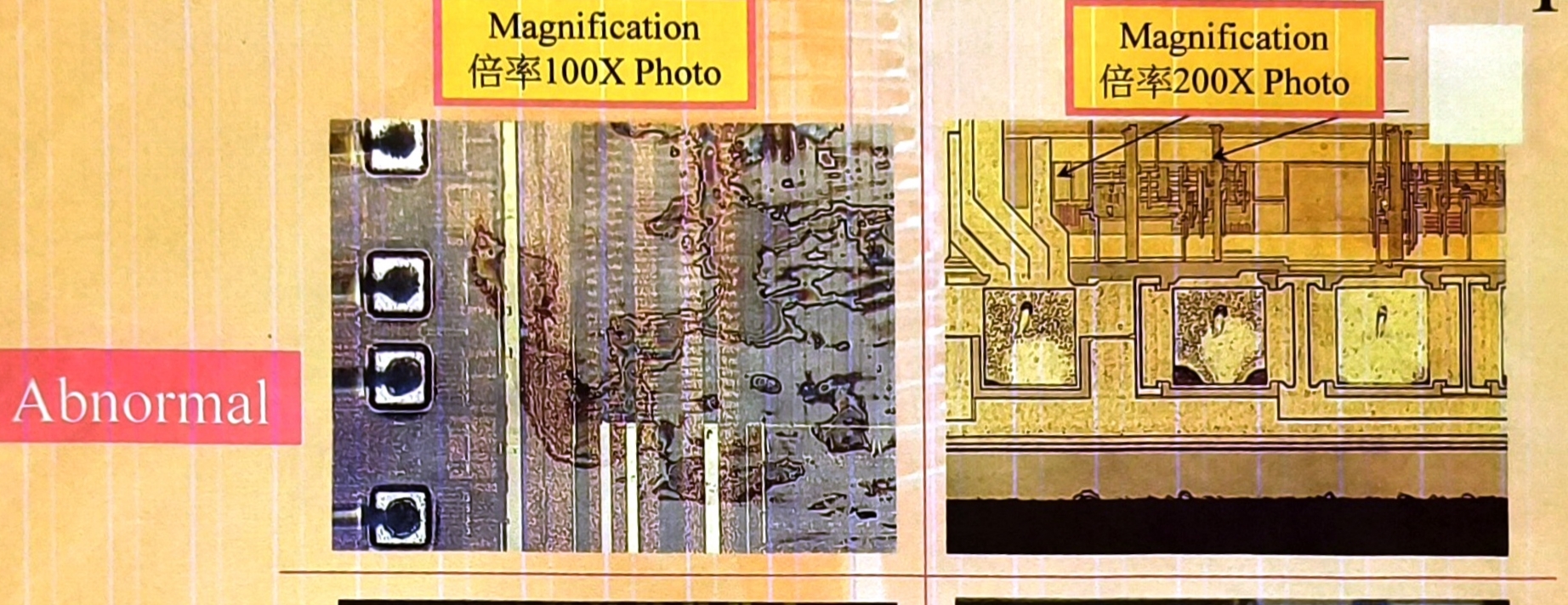
.
Contamination/Discoloration on Pads
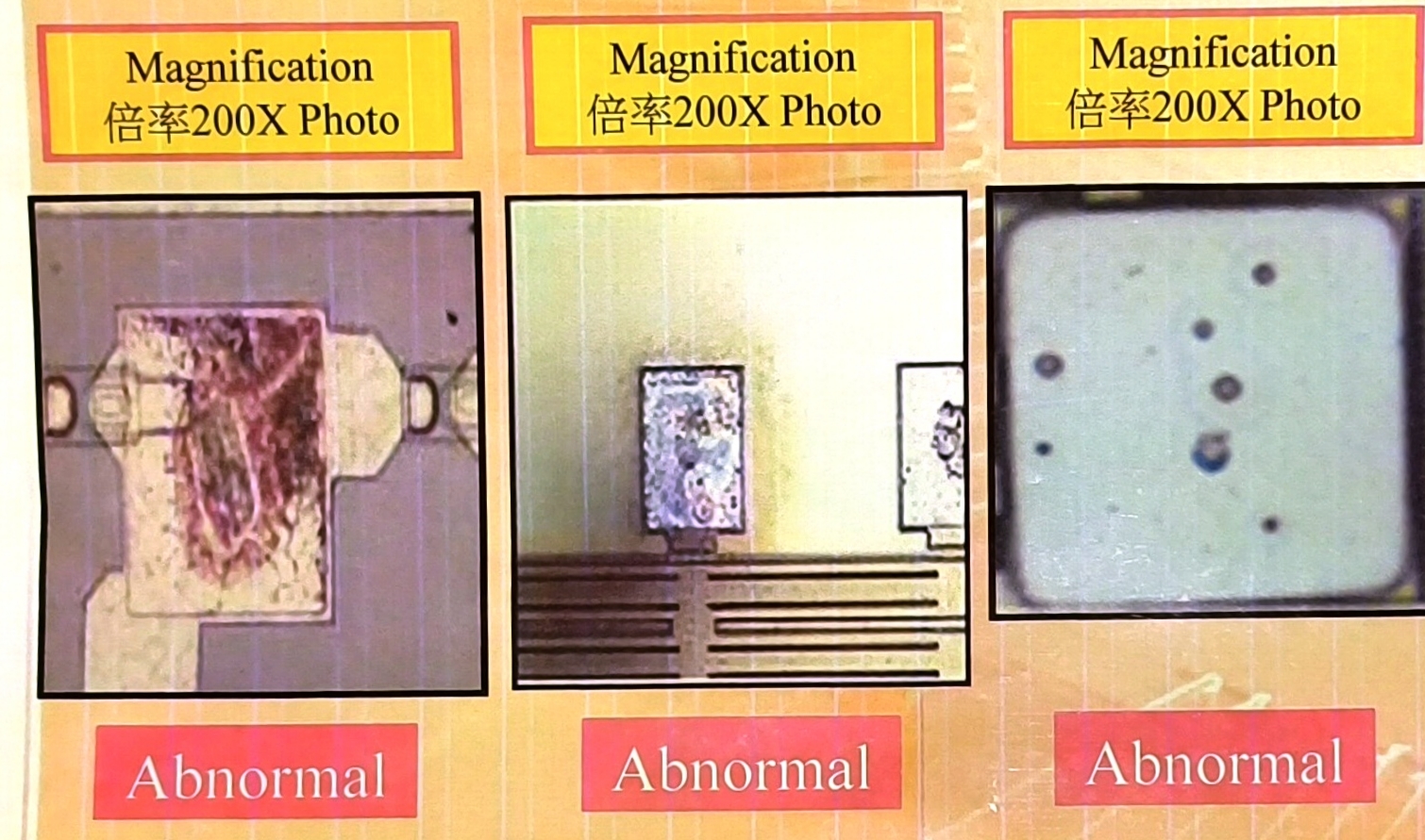
.
Oxidation/Corrosion on Pad
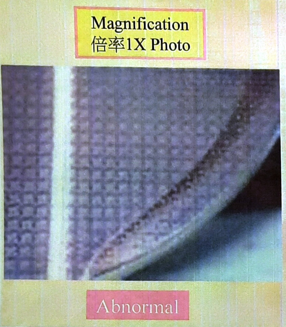
.
Contamination/Discoloration on Edge
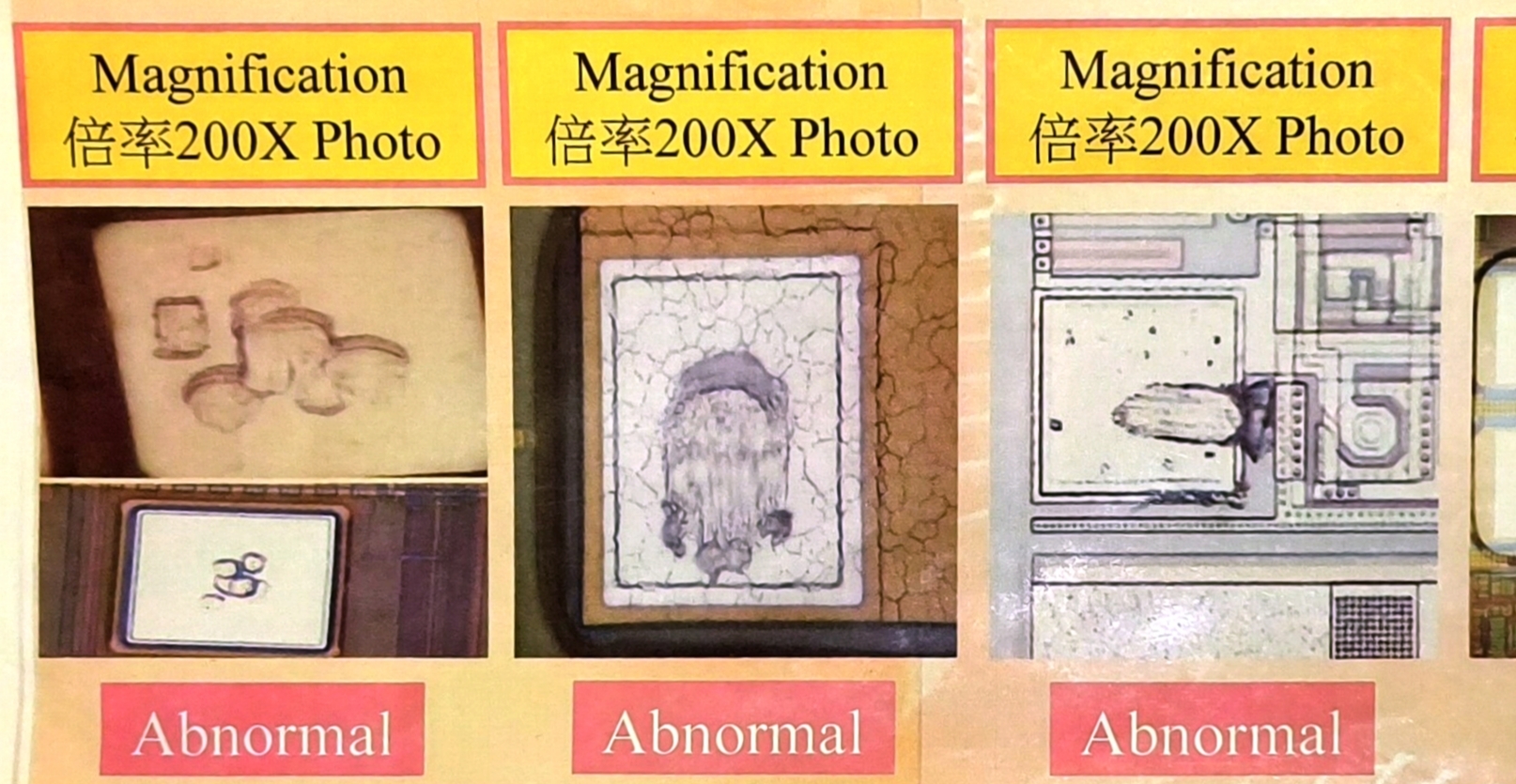
.
Probe mark defect
Probe Mark Not More than 3 times(reject over 3 times)(Reject probe mark exceed 25% Metallization) ( Reject Probe mark exceeded to metal)
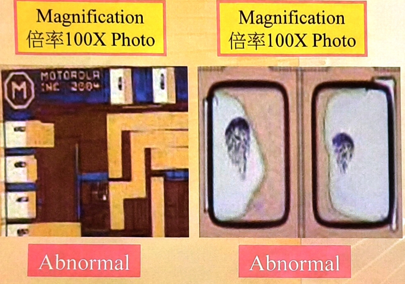
.
Passivation Mis-alignment/Opening Defect
If Passivation Covers more than 25% of bond pad area, it will be rejected
.
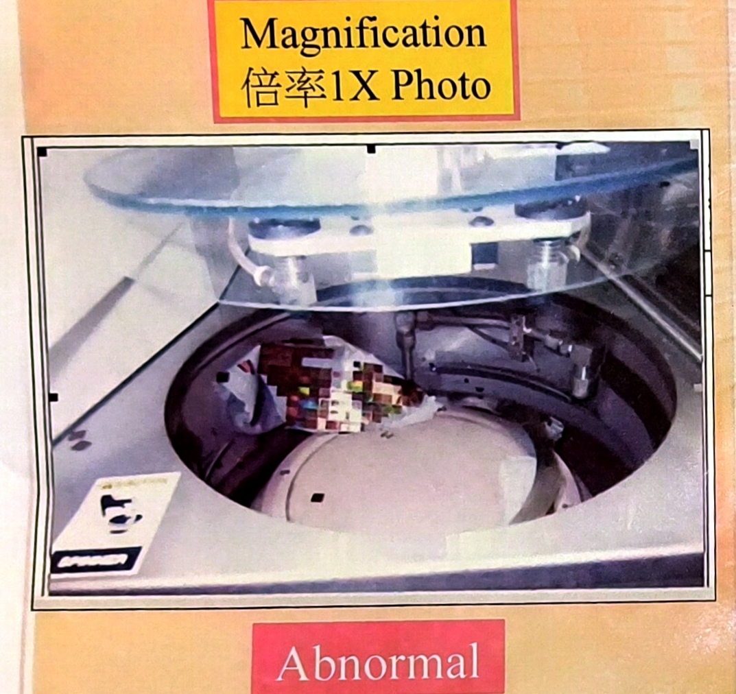
Tape Fall Off
.
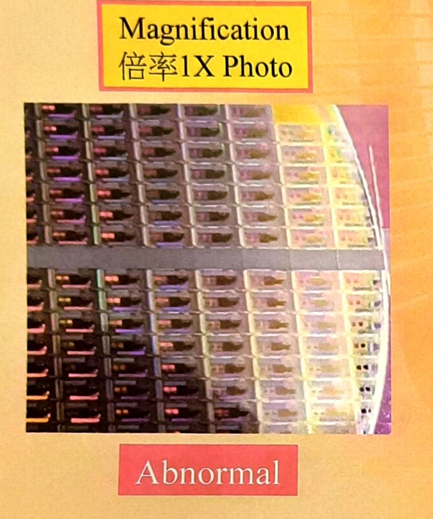
Dice Fly off
.
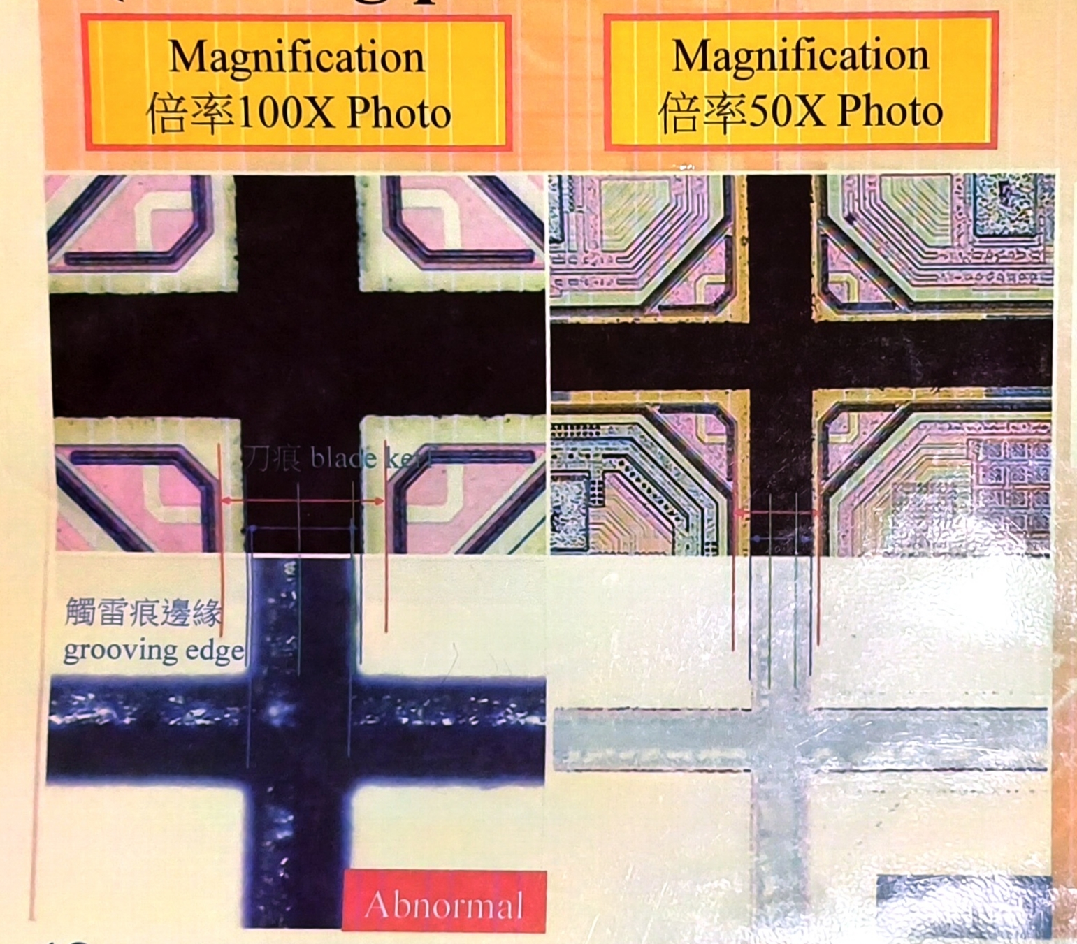
Cutting Performance of Laser Grooving
Need to check any abnormal of blade kerf shift for LG device and can not touch grooving edge)
.
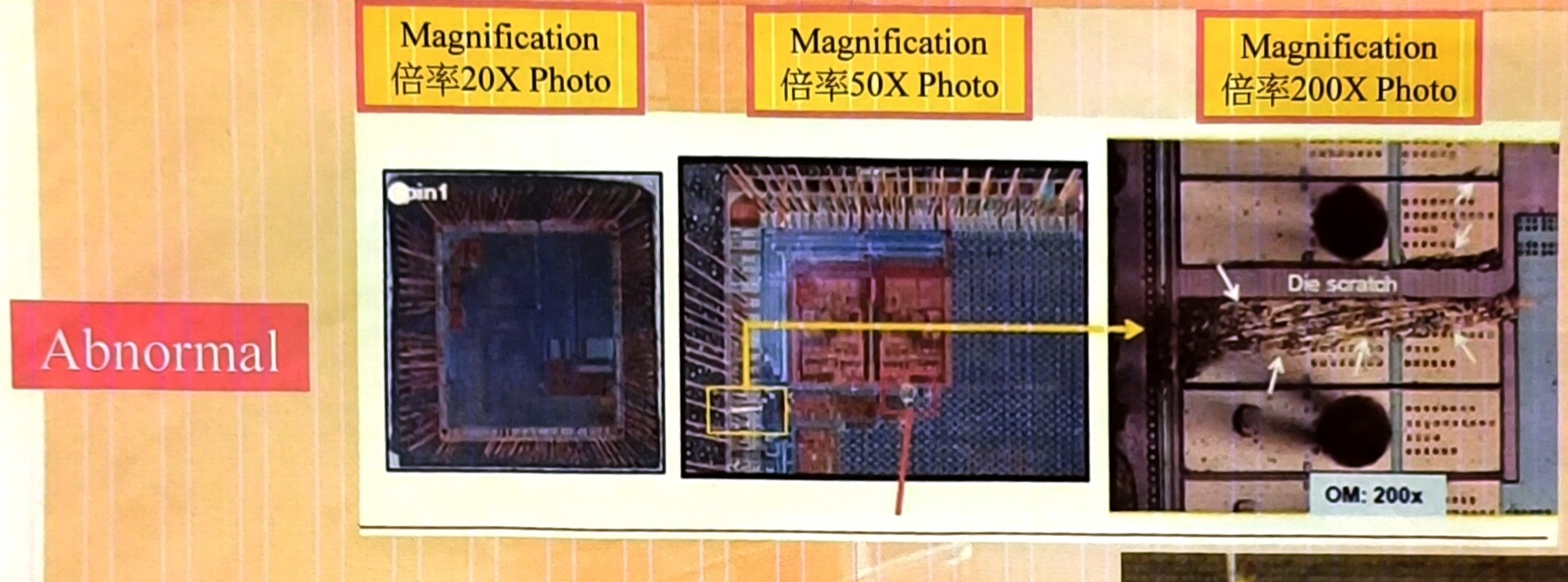
Surface Scratch
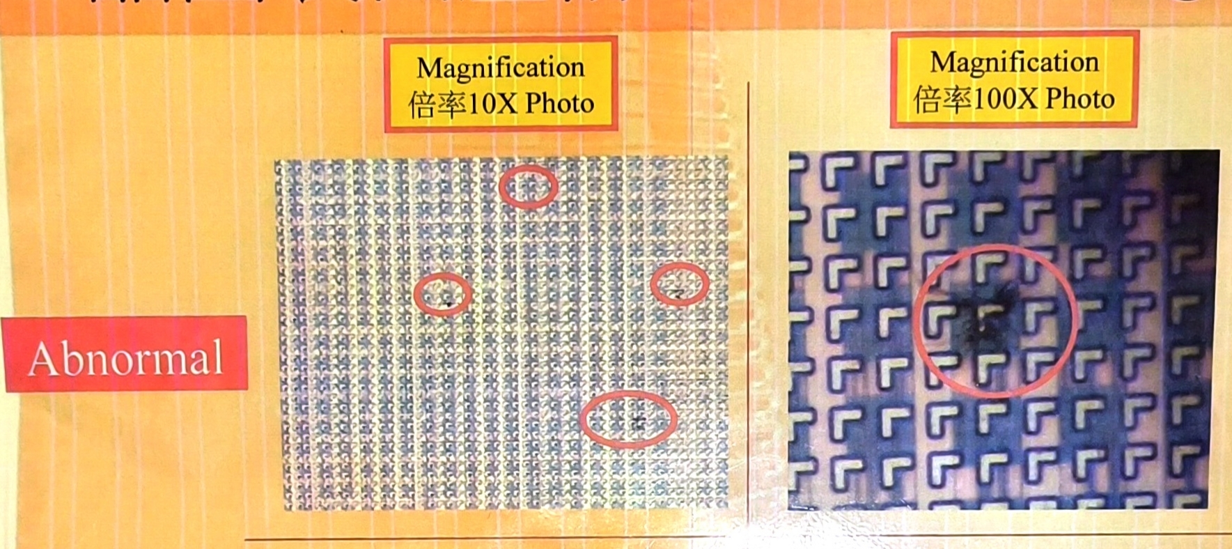
.
Surface Damaged
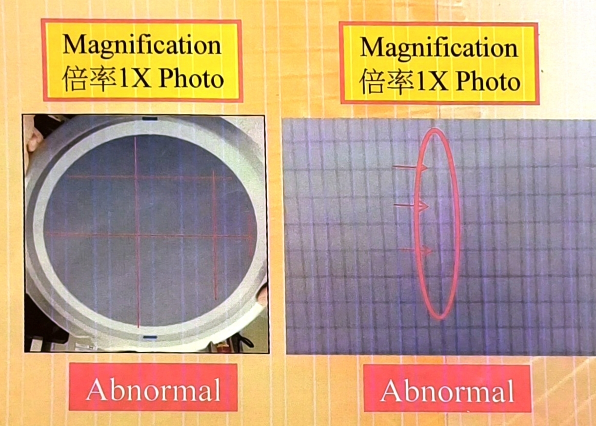
.
Seepage on Wafer
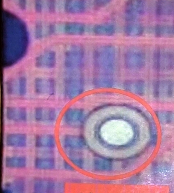
.
Missing Bump
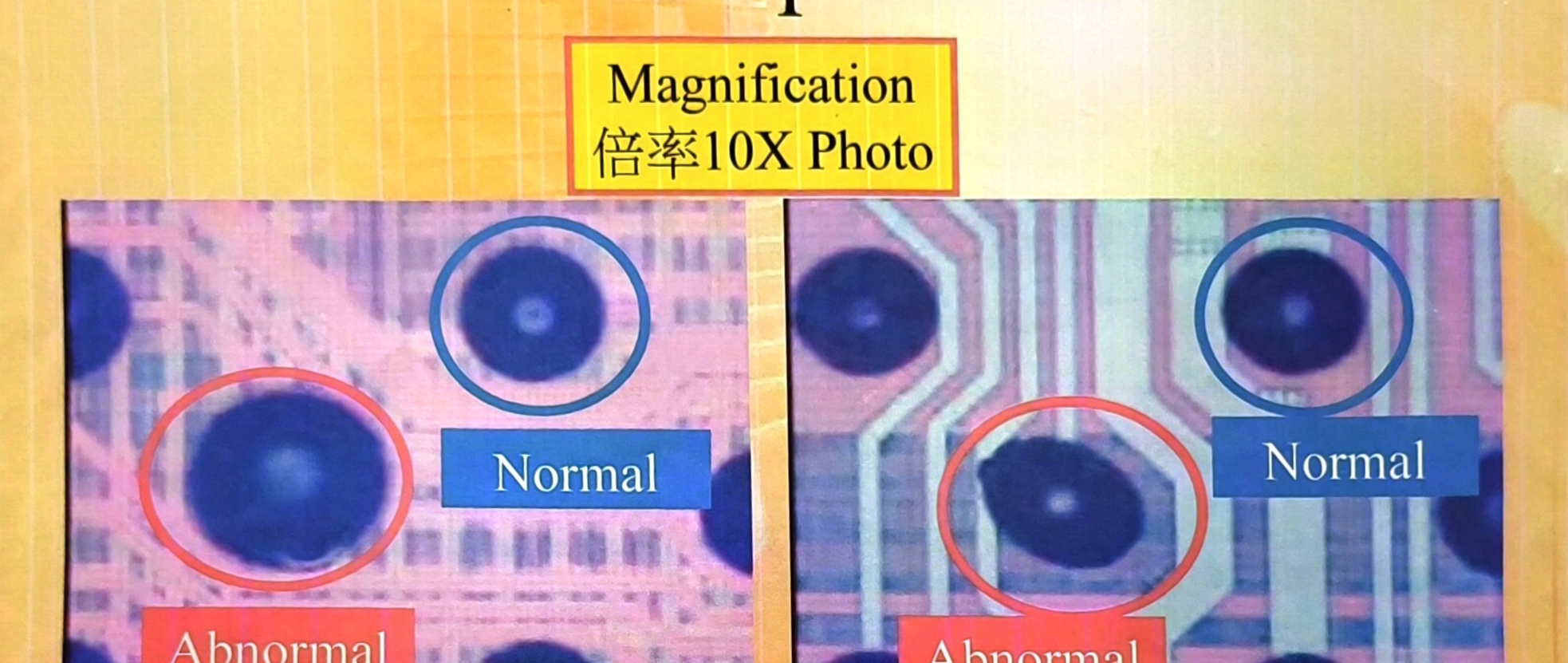
.
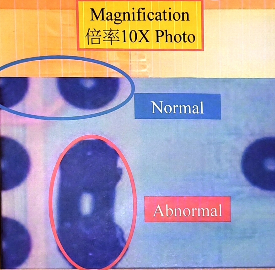
OR Irregular Bump
(reject ball dia. bigger or smaller than 25% of ball size
.
Bump Bridge

.
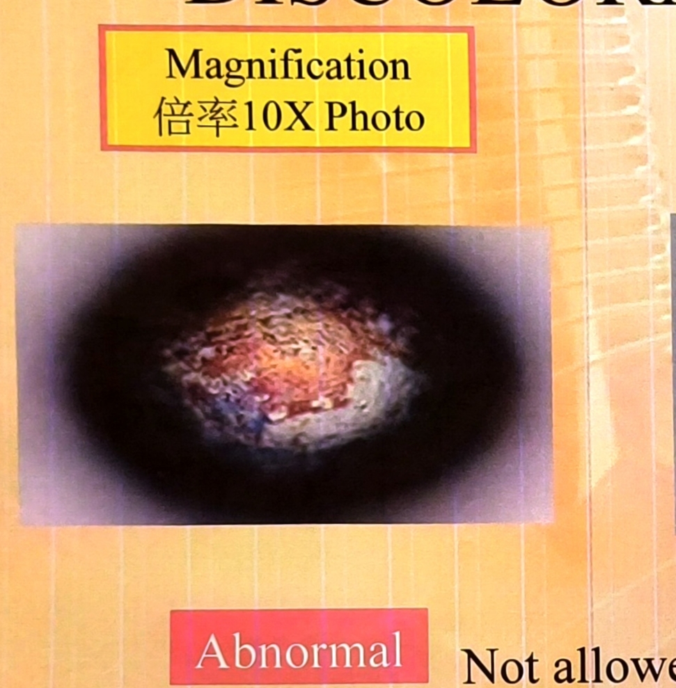
Damaged Bump
Reject Ball Damage < 15% ball height)
.
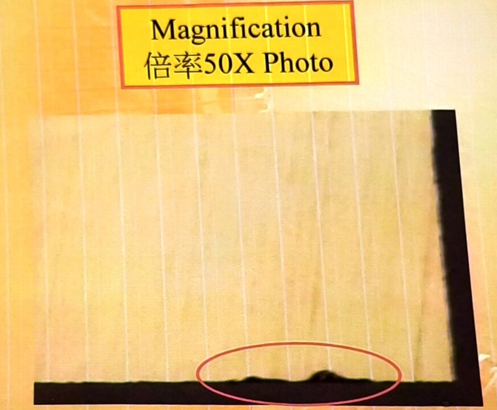
Wafer Ball Discoloration
.
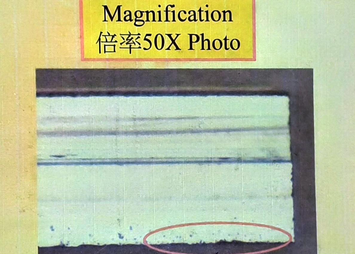
BackSide Chipping
backside chipping <= to 80um
.
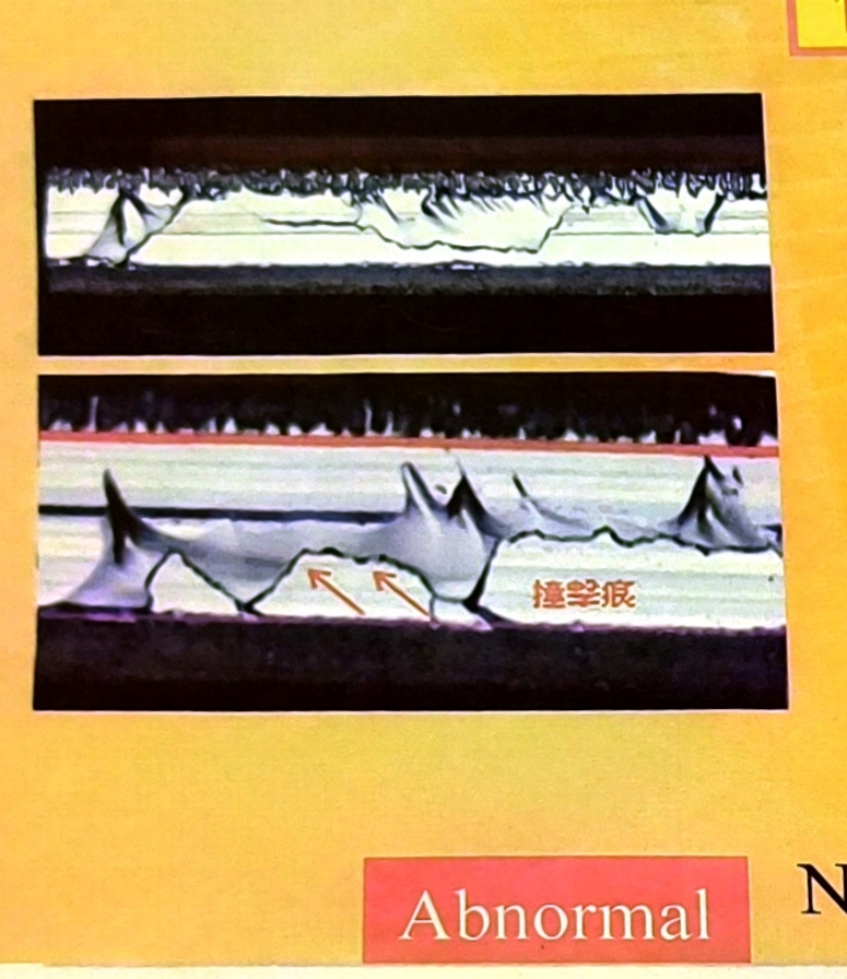
Side Chipping
(Wafer thickness > 4.7 mil, side chipping <= 60 um) (wafer thickness<= 4.7 mil,side chipping <= 1/2 wafer thickness)
.
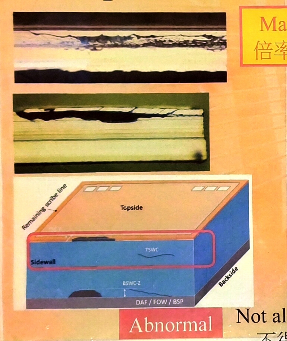
Sidewall Chipping / Crack
.
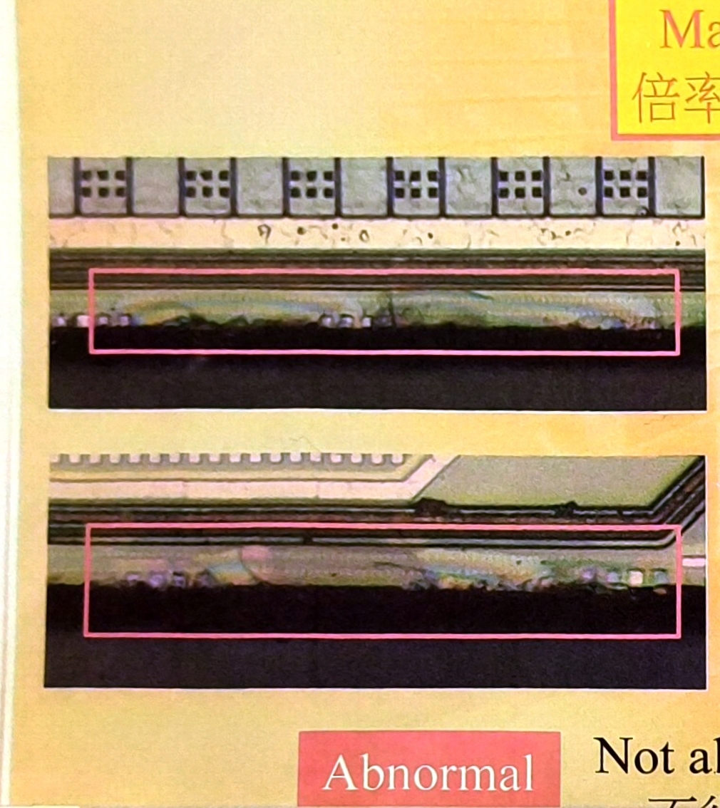
Top Sidewall Chipping / Crack
.
Discoloration (Delamination)
.
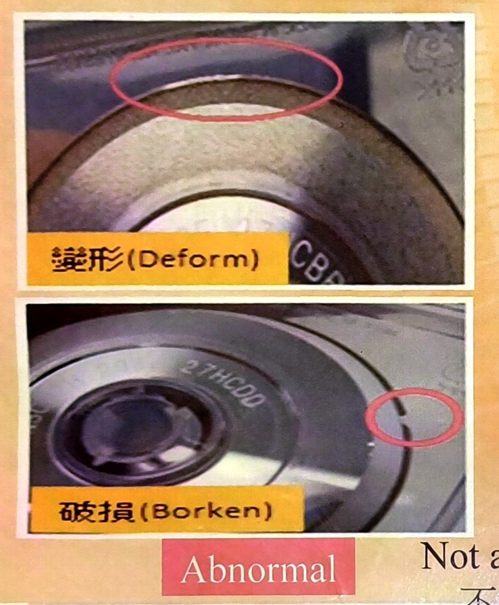
Blade Damage