COAL_FINALS
1/178
There's no tags or description
Looks like no tags are added yet.
Name | Mastery | Learn | Test | Matching | Spaced | Call with Kai |
|---|
No analytics yet
Send a link to your students to track their progress
179 Terms
SAP-1
Basic model of a microprocessor.
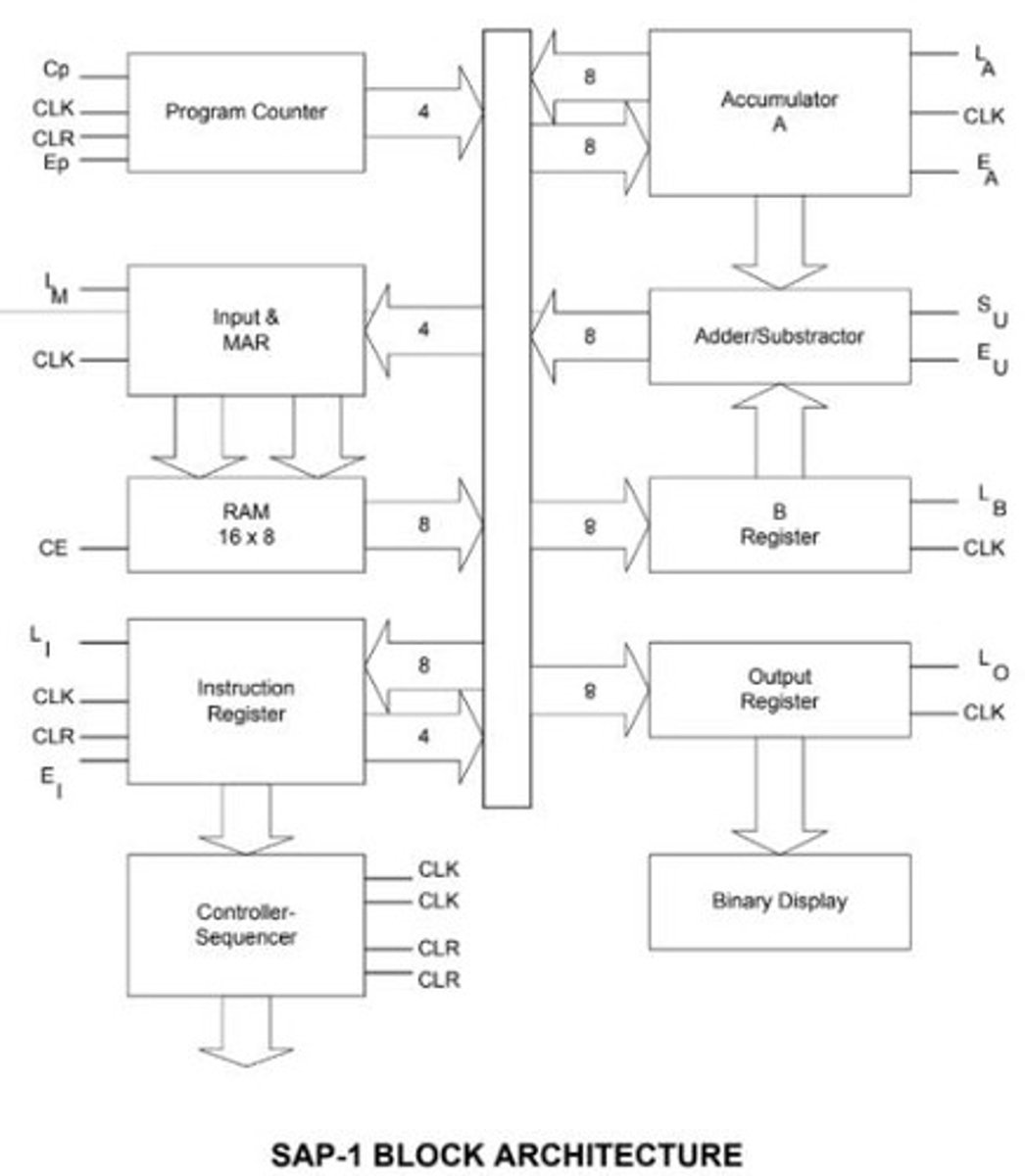
Program Counter
Counts from 0000 to 1111 for instructions.
Memory Address Register (MAR)
Stores memory addresses during execution.
RAM
Stores program code and data for execution.
W Bus
Single 8-bit bus for data transfer.
Accumulator
8-bit buffer for intermediate results.
B-Register
Holds the second operand for operations.
Instruction Register
Contains the current instruction to execute.
Output Register
Holds output from the OUT instruction.
Binary Register
Displays contents using eight LEDs.
Control Unit
Generates control signals for operation sequencing.
Adder/Subtracter
Performs addition and subtraction operations.
Instruction Set
Defines operations like LDA, ADD, SUB, OUT, HLT.
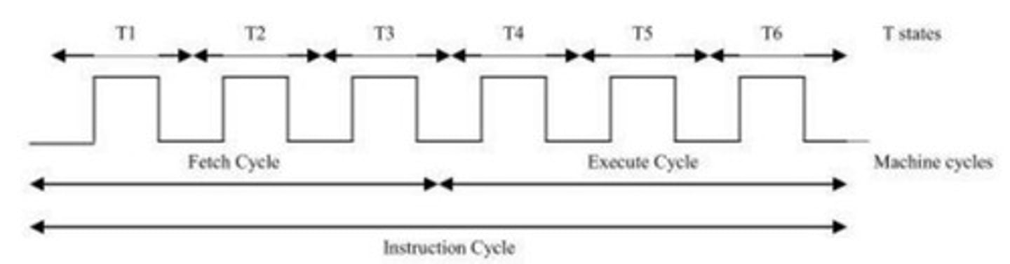
Instruction Cycle
Process to execute a single program instruction.
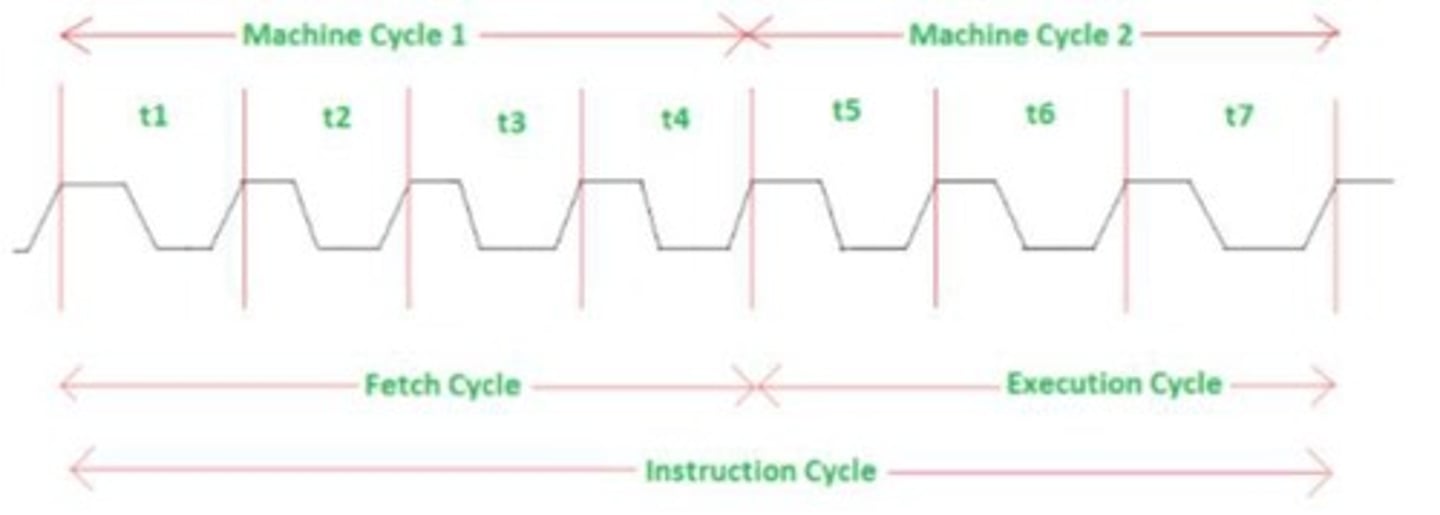
Machine Cycle
Part of the instruction cycle for execution.
Asynchronous RAM
Outputs data immediately upon valid address.
16x8 RAM
Contains 16 bytes of 8-bit memory.
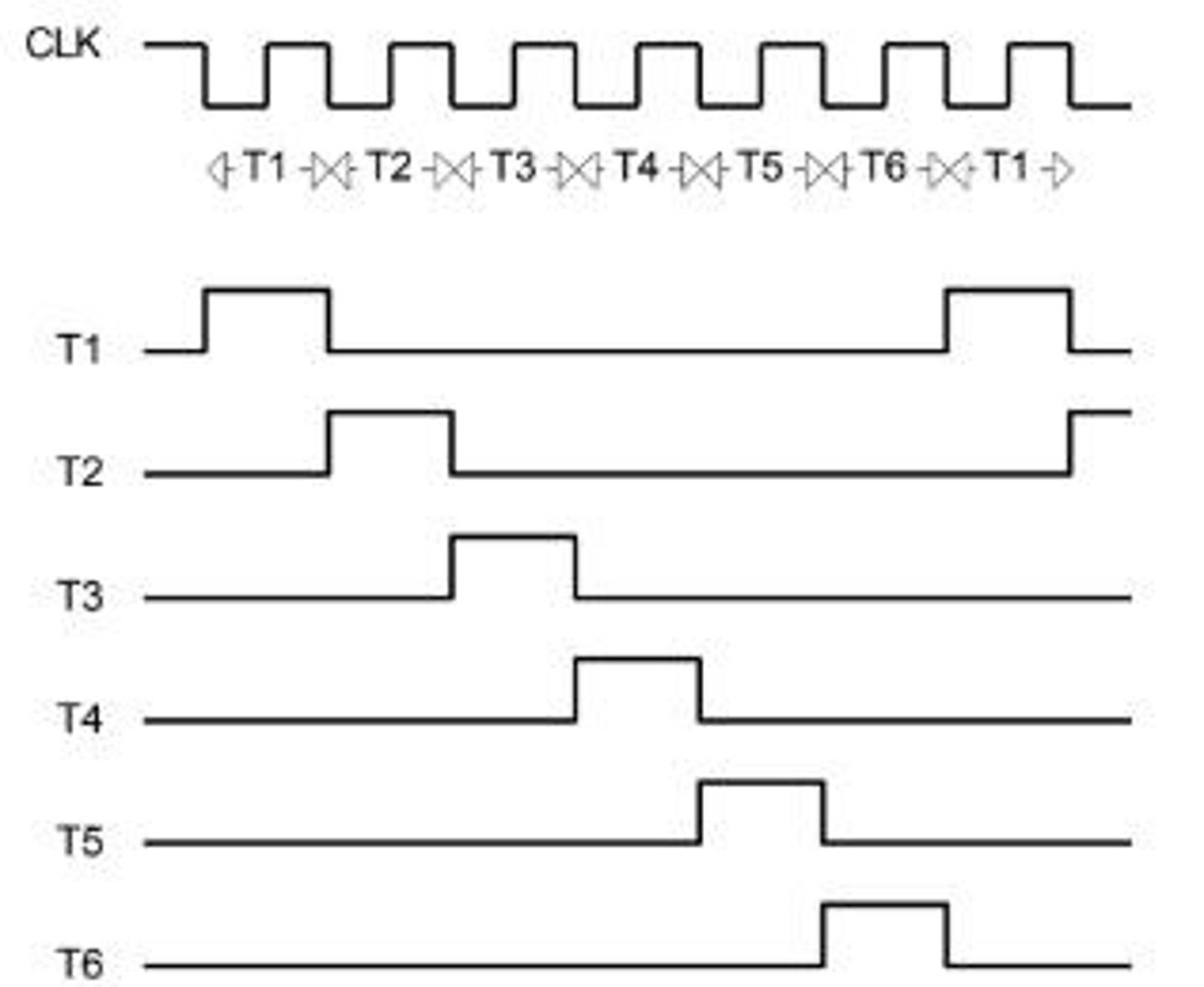
CLK Signal
Synchronizes operations in the SAP-1.
Control Word
Determines register reactions on CLK edge.
HLT Instruction
Halts the computer's processing.
12-bit Word
Output from the controller-sequencer block.
Simple Output Device
Binary display unit for SAP-1 microprocessor.
Fetch Cycle
Initial phase for instruction retrieval from memory.
Machine Cycle
Basic operational unit of CPU execution.
T-state
Specific time interval in instruction execution.
NOP Cycle
No Operation cycle, unused T-state.
Ring Counter
6-bit counter cycling through states 1-6.
PC (Program Counter)
Register holding address of next instruction.
MAR (Memory Address Register)
Holds address for memory access operations.
IR (Instruction Register)
Stores current instruction being executed.
Clock Pulse
Signal used to synchronize operations in circuits.
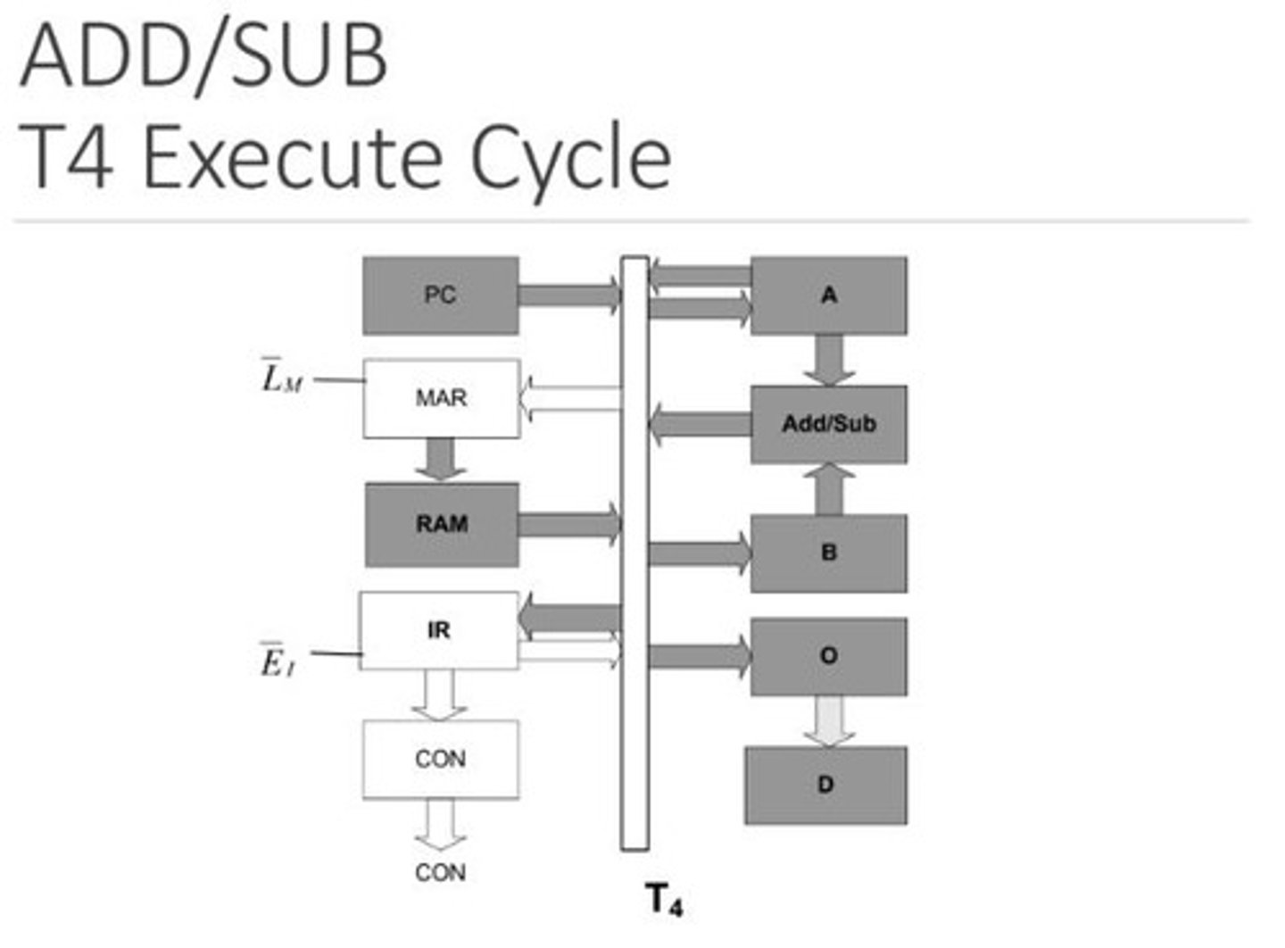
Execute Cycle
Phase where fetched instruction is executed.
Opcode
Operation code defining specific instruction to execute.
Operand
Data or address used by the instruction.
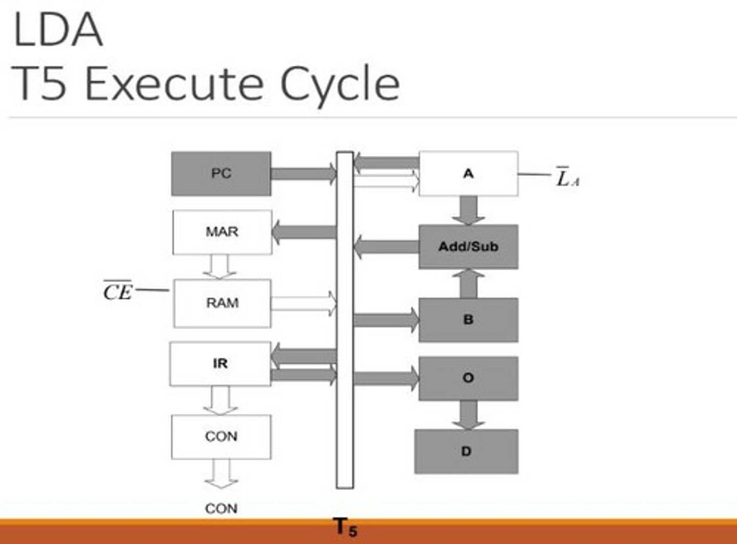
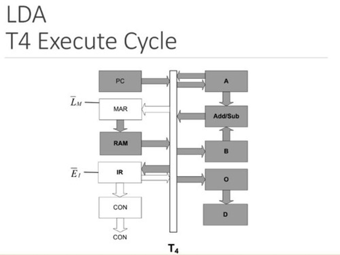
LDA Instruction
Load accumulator with data from memory.
Accumulator
Register storing intermediate arithmetic and logic results.
ALU (Arithmetic Logic Unit)
Performs arithmetic and logical operations.
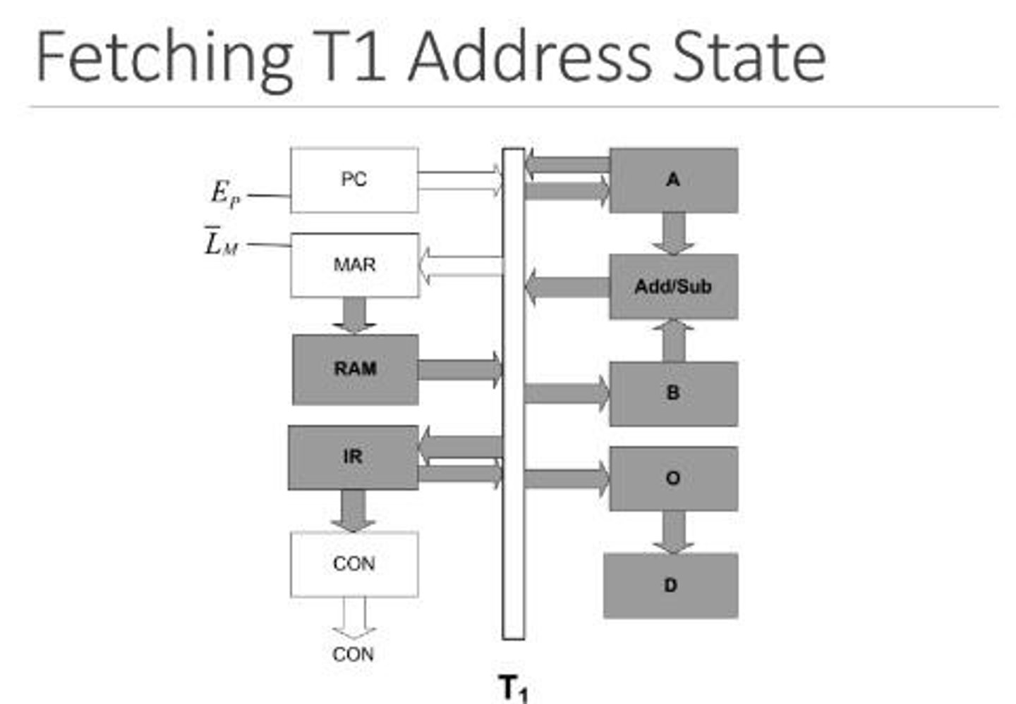
Address State
T1 state enabling address output to bus.
Increment State
T2 state incrementing program counter value.
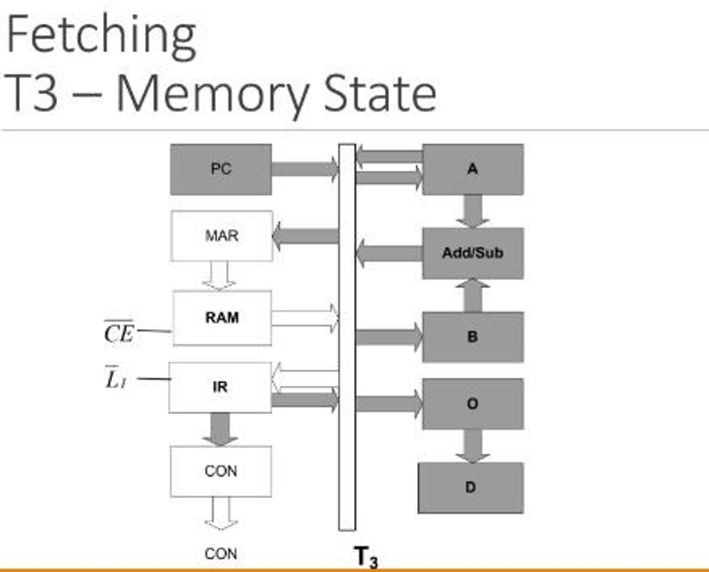
Memory State
T3 state enabling memory access for instruction.
Execution Cycle
Includes T4, T5, T6 for instruction execution.
Arithmetic Operations Limit
SAP-1 limited to seven arithmetic operations.
Maximum Value Limit
SAP-1 can handle numbers up to 255.
Addressing Mode
SAP-1 uses addressed-mode for instruction execution.
Microcontroller
A micro-computer on a single silicon chip.
CPU
Central Processing Unit, executes instructions.
RAM
Temporary memory for data during execution.
ROM
Permanent memory for storing firmware.
I/O Port
Interface for communication with peripherals.
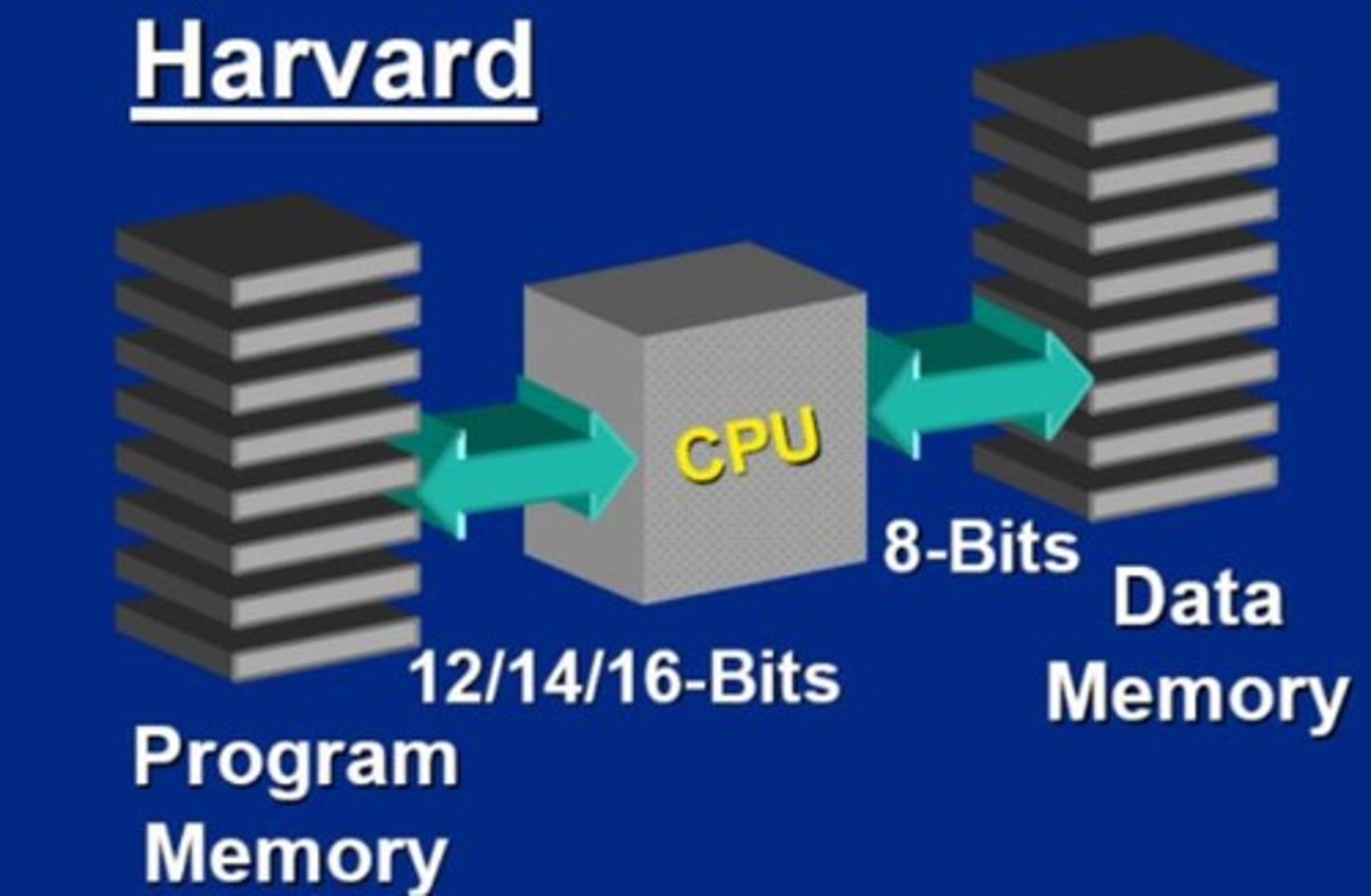
Harvard Architecture
Separate memory spaces for instructions and data.
RISC
Reduced Instruction Set Computer architecture.
CISC
Complex Instruction Set Computer architecture.
PIC
Peripheral Interface Chip, user-friendly microcontroller.
FLASH Memory
Rewritable memory for program storage.
EEPROM
Non-volatile memory for important data retention.
RAM Characteristics
Used for temporary data storage during runtime.
PORTA
Physical connection with five pins on MCU.
PORTB
Physical connection with eight pins on MCU.
Interrupt Sources
Triggers for CPU to pause current execution.
Free-Run Timer
Independent timer register within microcontroller.
Clock Generator
Provides timing signals for microcontroller operations.
PIC16F84A
8-bit microcontroller with RISC architecture.
Program Memory
Storage for written programs in FLASH.
Data Memory
Storage for data in RAM and EEPROM.
Special Function Registers
Registers for specific control functions in MCU.
Oscillator Types
Different methods for generating clock signals.
Crystal Oscillator
Metal housing component for precise timing.
Increment Value
Counts up to 255, then resets to zero.
Timer Function
Measures time intervals for device operations.
CPU Role
Connective element with frequency pins.
Ceramic Capacitor
30pF capacitor connected to oscillator pins.
RC Oscillator
Saves costs during microcontroller purchase.
Resonant Frequency
Depends on voltage, resistance, capacity, temperature.
Process Variations
Affects resonant frequency tolerances.
Ceramic Resonator
Oscillator and capacitors in a joint case.
MCLR Pin
Resets microcontroller to known conditions.
Resistor Range
5k to 10k for MCLR connection.
Pull Up Resistor
Maintains logical one state on a line.
Oscillator Placement
Should be near microcontroller to reduce interference.
Program Memory
First memory block in PIC16F84A architecture.
Data Memory
Second memory block in PIC16F84A architecture.
EEPROM Memory
64 eight-bit locations, non-volatile storage.
Indirect Access
Access EEPROM through EEADR and EEDATA registers.
Power-On Reset (POR)
Resets microcontroller upon power-up.
Watchdog Timer (WDT)
Resets during overflow to prevent hangs.
General Purpose Registers (GPR)
Banked RAM for greater than 116 bytes.
Special Purpose Registers (SFR)
Control registers for peripheral functions.
RAM Memory
Occupies space from 0x0C to 0x4F.
GPR
General Purpose Registers in microcontroller.
Subroutine
Reusable code section called as needed.
Port
Register for microcontroller pin connections.
TRIS Register
Defines pin as input or output.
PIC16F84A
Microcontroller with 35 instruction set.
Instruction Set
14-bit word with OPCODE and operands.
Byte-Oriented Operations
Operations involving entire bytes of data.
Bit-Oriented Operations
Operations affecting individual bits in registers.
EQU Command
Assigns a name to a register address.
Delay Loops
Counts down to create time delays.
Header Comment
Descriptive comment at the beginning of code.
Directive
Instruction for the assembler, not the PIC.