CSCI 50.01 LT#3
1/249
There's no tags or description
Looks like no tags are added yet.
Name | Mastery | Learn | Test | Matching | Spaced | Call with Kai |
|---|
No analytics yet
Send a link to your students to track their progress
250 Terms
Datapath
Hardware components that execute instructions
What does Main Memory contain?
instructions to execute any data (ex. variables)
Give an address to either: ______ or _______
1. Retrieve a line of code/data
- Address specifies location containing instructions & parameters, or contents of variable
2. Overwrite a line of data
- Contents of variable
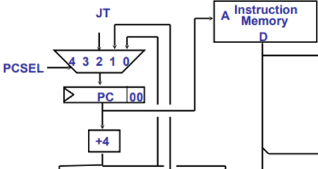
Address in Program Counter (PC)
Passed to instruction memory to fetch next instruction to be executed
Main memory should have at least ____ read port/s and ______ write port/s
2 read ports
1 write port
Program Counter
1 instance of main memory
Knowing where you are requires a register (esp for branching or jumping)
Opcode
Binary code
Represents specific instruction
What is the purpose of assigning opcodes to instructions?
to identify instructions for processor to differentiate operations
assigned based on functional groups or specific criteria
What pattern is used for arithmetic instructions in the Beta instruction set?
- Using constants have opcode[4] == 1
- Using 2nd register have opcode[4] == 0
What is the opcode significance of branching instructions like BEQ or BNE?
use constant to specify branch target address, so opcode[4] == 1
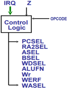
Control Unit
- Given instruction's opcode
- Sends signals to rest of CPU for instruction execution
Registers
Storage in CPU for temporary variables passed to ALU
Includes PC to remember address of next instruction
Register File
- Collection of registers for instruction arguments
- Used for Ra/Rb/Rc arguments in BSim implementation
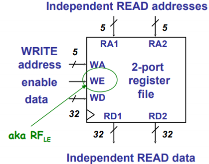
RFLE
Register File Load Enable (allow write)
OPCODE Fields
Operate: ADD, ADDC
Main memory: LD, ST
Program control: JMP, BEQ
How are Incremental Design datapaths implemented?
Implement datapaths for each class individually
Merge datapaths (old functionality maintained while adding new functionality)
Instruction Fetch
Process of retrieving next instruction
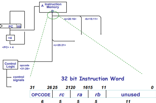
Instruction Fetch Steps
PC passes address of current instruction to main memory
Default next instruction is in next line (address + 4)
Instruction's opcode passed to control logic
Control logic send signals to execute current instruction
Is it necessary to "save" PC's value?
Yes
Can the system function without a PC register?
No assuming PC is not saved anywhere
Is there another way to remember where we are in the program and to send the appropriate address to main memory for instruction fetch?
Yes only if PC is saved somewhere (doesn't have to be a register) in a device connected to main memory's instruction port's address
What is the role of control logic in a processor?
determines what ALU should do
controls if overwriting is allowed in register file for current instruction
What input does the register file receive from an instruction?
register addresses specified in instruction
What does the ALU base its operations on?
Instructions from control logic
WERF
Write Enable Register File
Controls if current instruction can overwrite a register in register file
1 - can overwrite
0 - can’t overwrite
Why can't WERF be don't care (1)?
Setting it to 1 (DC) will cause an unspecified overwrite to occur because of how registers function
ALUFN
Arithmetic and Logic Unit FunctioN
ALUFN
Arithmetic and Logic Unit FunctioN
Specifies operation that ALU should perform
How to send A and B inputs to the ALU without using a register file?
A and B inputs sent to ALU directly via connections to main memory instead of register file
What issues arise when sending ALU inputs directly from main memory?
More bits needed to specify memory addresses:
- Register file uses 5 bits (for 32 registers)
- Main memory with 2^20 lines would require 20 bits for address specification
What does BSEL do in ALU operations?
selects either:
- Rb (register file input)
- Constant embedded in the instruction
What must be done to a 16-bit constant before it can be used in ALU operations?
SEXT
sign-extended to 32 bits to match the ALU's input size
How does the current setup support both ALU register-register and register-constant operations?
Can choose between:
- Rb (register input) for register-register
- Constant (from instruction) for register-constant
What role does the multiplexer controlled by BSEL play in ALU operations?
Switches ALU's B input between
- Value from register file (Rb)
- Sign-extended constant from instruction
BSEL
B Selector
WDSEL
Write Data SELector
Controls source of data written to register file's Rc port
"What am I supposed to write to register file?
Possible Values of BSEL
0 - need Rb's data to be passed, ignore constant (c[15:0])
1 - need their attached 16-bit constant, ignore Rb
How do you sign-extend a 16-bit value to a 32-bit value?
- Copy most significant bit into rest of the bits
- This preserves the sign
Why do memory and branching instructions have opcode[4] = 1?
They require a constant
EX. for addresses or offsets
What are examples of arithmetic instructions using a second register in the Beta instruction set?
ADD, SUB, and MUL
How are opcodes grouped in Beta instruction set?
Based on functionality, with specific opcode bits (like opcode[4]) indicating if constant or second register
How does BSEL allow Rb[15:11] and c[15:0] to occupy the same space in an instruction?
Uses mux to enable either rb[15:11] or c[15:0] as active input
Ensure only 1 path is used despite sharing instruction space
What is BSEL for?
Controls what gets passed as ALU's B input
WDSEL Possible Values
0: For BEQ/BNE
1: ALU output
2: Main memory's data read port's data
Wr
Write to memory
What is Wr used for?
- to know if reading or writing to main memory
- Similar to WERF, but specifically for memory writes
Possible Values of Wr
0: No data written to memory
1: Data written to memory.
For LD instructions, what should ALUFN be?
ADD
LD calculates address by adding <Ra> and C using ADDC
For LD instructions, what should BSEL be?
1
LD uses constant as second 2nd operand
For LD instructions, what should WDSEL be?
2
Data is read from main memory and written to register file's Rc
For LD instructions, what should Wr be?
0
LD doesn't write to main memory
RA2SEL
Read Address #2 SELector
determines which address is used for 2nd register
RA2SEL possible values
0 - Use Rb[15:11]
1 - Use Rc[25:21]
For ST instructions, what should ALUFN be?
ADD
ST calculates memory address by <Ra> + C using ADDC
For ST instructions, what should BSEL be?
1
ST uses constant (C) as second operand for ALU
For ST instructions, what should WERF be?
0
ST doesn't write to register file
For ST instructions, what should WDSEL be?
DC
WDSEL is not used for ST bc WERF = 0
0 default value for WDSEL
For ST instructions, what should Wr be?
1
ST writes data from Rc to main memory[<Ra> + C]
For ST instructions, what should RA2SEL be?
1
ST reads data from Rc[25:21] for writing to memory
What should RA2SEL be for non-ST instructions?
0 - read from Rb[15:11]
DC - don't read from Rb or Rc
Why does ST use Rc[25:21] instead of Rb[15:11]?
Because it needs a constant C[15:0] and can’t use Rb[15:11] simultaneously
PCSEL
Program Counter SELector
What is PCSEL used for?
determines the next instruction address
Possible Values of PCSEL
0 - Use default PC + 4
1 - Use branch address
2 - Use <Ra> for JMP instructions
can have 3 or 4 as well (but idk for what)
For JMP instructions, what should WDSEL be?
0
Passes PC + 4 to be written to Rc as return point
For JMP instructions, what should ALUFN be?
Dont care
For JMP instructions, what should BSEL be?
Don’t care
For JMP instructions, what should WERF be?
1
JMP writes PC + 4 to register file (Rc) as return point
What is Z for?
Zero check
1 if <Ra> is 0
0 otherwise
Requires additional circuitry to check if <Ra> is zero
For BEQ instructions, what should PCSEL be?
PCSEL = Z
0 if Z = 0
1 if Z = 1 (branch)
For BNE instructions, what should PCSEL be?
PCSEL = !Z
1 if Z = 0 (branch if <Ra> ≠ 0)
0 if Z = 1 (don't branch).
For both BEQ/BNE instructions:
What should ALUFN be?
What should WDSEL be?
What should WERF be?
ALUFN = DC
WDSEL = 0 (passes <PC>+4 to be written to Rc)
WERF = 1
What is XP (R30) used for?
register for handling Interrupts or Exceptions
Examples of CPU or system-generated faults (synchronous)
- Illegal instruction
- System calls, like "read-a-character"
Examples of externally generated I/O events (asynchronous)
Interrupt Request (IRQ) events like a key being pressed
How Interrupts Work:
1. Interrupt running program
2. Invoke exception handler (Similar to a procedure call)
3. Return to continue execution
What does ILLOP (PCSEL = 3) handle?
Handles illegal operations, like:
- Divide by 0
- Unimplemented instructions
What happens during an illegal instruction?
1. Procedure call is forced
2. CPU branches to illegal operation handler instead of executing illegal instruction
3. <PC+4> is saved to XP (R30)
4. Program resumes at instruction after illegal one
What does XAdr (PCSEL = 4) handle?
Interrupt Requests (IRQs)
What happens during an interrupt request?
1. Procedure call is forced
2. CPU branches to IRQ handler
3. <PC> is saved to XP (R30)
4. Program resumes at instruction that was supposed to execute when interrupt occurred
What is the difference between ILLOP and XAdr in handling events?
ILLOP handles illegal operations, saving <PC+4> to XP (R30)
XAdr handles interrupts, saving <PC> to XP (R30)
What is the primary purpose of a cache in a memory system?
combines high-speed memory access of expensive memory with large size of cheaper, slower main memory
How does a cache improve memory access efficiency?
Storing copy of frequently accessed portions of main memory for future use
Take advantage of locality of reference
Cache Read Operation
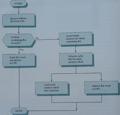
What happens when the processor attempts to read a word of memory?
Check if word is in cache
Cache Hit
- requested word is in cache
- it's delivered to processor
What happens during a cache hit?
- Address & data buffers disabled
- Communication only between processor and cache
- No system bus traffic
Cache Miss
Requested word not in cache
Desired address loaded onto system bus
Data is returned via data buffer to cache & processor
Why does cache load a block of memory instead of requesting the word during a miss?
To take advantage of locality of reference, which predicts that nearby words might be accessed soon
How many addressable words are in main memory?
2n addressable words
each word having a unique n-bit address
What are blocks in main memory?
Main memory is divided into fixed-length blocks, each containing K words
How many blocks (M) are in main memory? (formula)
M blocks in main mem = (2n) / K words
Cache consists of C blocks called ___?
Lines
Each line contains ______ words and additional information like ______ and ______
K words
Tags and Control bits
Tag identifies …?
- Identifies which block is currently being stored
- Equivalent to part of the block's memory address
What additional information is stored in a cache line besides words and tags?
Control bits to indicate if line was modified since being loaded into cache
What is the line size in a cache?
length of a line in cache, excluding tag and control bits
How does number of cache lines C compare to number of main memory blocks M?
lines C < main memory blocks M
A single cache line can hold data from multiple main memory blocks simultaneously
False
True or False: Every block in main memory has a dedicated cache line in the cache.
False