Lec1 Intro. Wafer + Evaporation | NTU MS3012
1/70
There's no tags or description
Looks like no tags are added yet.
Name | Mastery | Learn | Test | Matching | Spaced | Call with Kai |
|---|
No analytics yet
Send a link to your students to track their progress
71 Terms
Which of the following processes (involved in the fabrication of Si wafers from raw materials) are arranged in the correct order?
Formation of electronic grade silicon → Formation of metallic grade silicon → Czochralski process → Dicing
Formation of metallic grade silicon → Formation of electronic grade silicon → Czochralski process → Dicing
SiHCl3 purification → Formation of metallic grade silicon → Czochralski process → Dicing
SiHCl3 reduction → Formation of metallic grade silicon → Czochralski process → Dicing
Formation of metallic grade silicon → Formation of electronic grade silicon → Czochralski process → Dicing
What process is used for depositing photoresist on the Si wafer?
Evaporation
Polymerisation
Spincoating
Crosslinking
Spincoating
Please indicate whether the following statement is true or false: A positive photoresist is an organic polymer that becomes harder to dissolve when light falls on it.
False (negative photoresist is harder to dissolve when light hits it)
Please indicate whether the following statement is true or false: Undercutting is a problem caused due to isotropic etching.
True
Please indicate whether the following statement is true or false: Packaging is done only for mechanical support and environmental protection of the Integrated circuit.
False
Which of the following is not an advantage of e-beam evaporation over physical evaporation for the formation of thin films?
Cleaner deposition and therefore purer film
Able to evaporate high melting point materials
More efficient heating technique
Can be performed at higher pressures
Can be performed at higher pressures
The reaction “e* + Ar → Ar+ + e + e” is best classified under which of the following categories?
Dissociation
Molecular ionisation
Atomic excitation
Atomic ionisation
Atomic ionisation
Please indicate whether the following statement is true or false: DC sputtering is utilized only for non-conducting substrates.
False
Please indicate whether the following statement is true or false: Magnetron sputtering involves localisation of the electrons close to the target surface in order to more efficiently generate plasma.
True
Please indicate whether the following statement is true or false: Sputtering normally forms thin films with a morphology consisting of small grains.
True
The conducting channel of an NMOS transistor is composed of…
Electrons
A PMOS TRANSISTOR OPERATES UNDER THE FOLLOWING VOLTAGE BIASING CONDITIONS
VGS=-ve, VDS=-ve
Which of the characteristics of thin films need to be carefully controlled (ideally)?
Thickness, Compositional Uniformity (low number of impurities and defects), Conformal coverage (accounts for steps on the surface), Planarity (quality of being flat/in a plane - important for building multilayers)
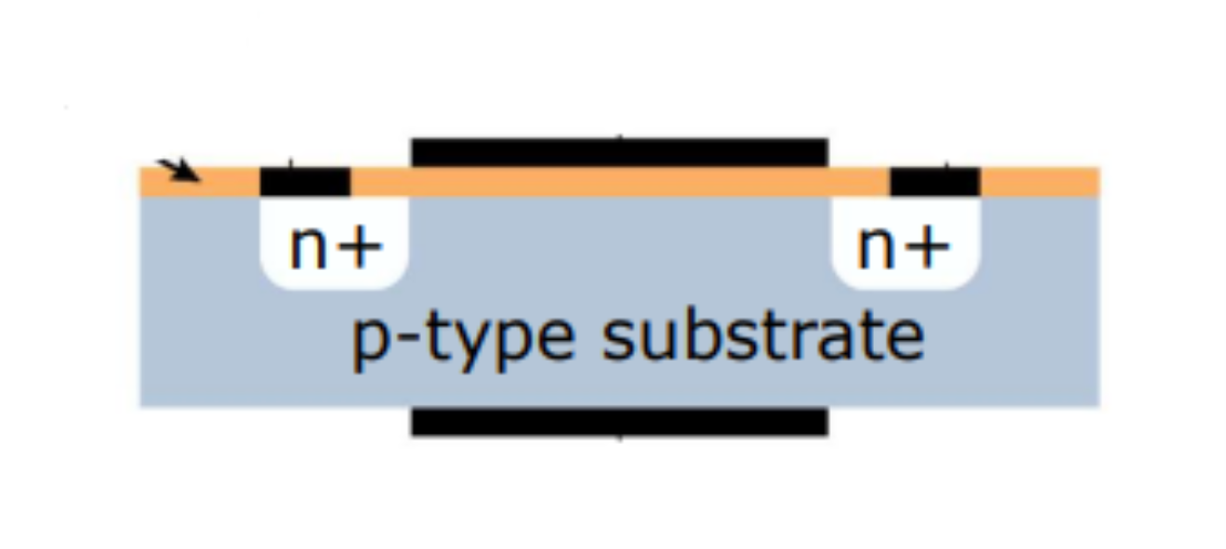
Is the following a n-type or p-type MOSFET?
n-type
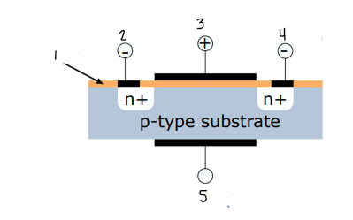
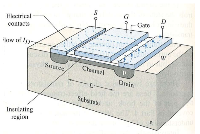
Label the following 1-5 and state whether it’s a n-type or p-type MOSFET
Oxide Layer
Source (S)
Gate (G)
Drain (D)
Body (B)
n-type (negatively-charged carriers)
The conducting channel of an PMOS transistor is composed of…
holes (positively-charged carriers)
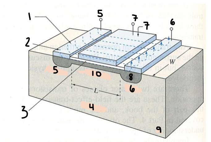
Label the following 1-9 on the PMOS
Electrical Contacts
Flow of ID
Insulating region
Substrate
Source (Source of charge carriers)
Drain (where charge carriers are drained)
Gate
p (positively-charged carriers = holes)
n
Channel
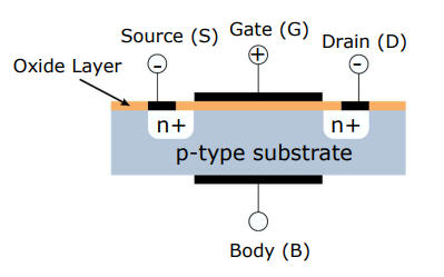
Define MOSFET
Metal-oxide-semiconductor field-effect transistor
(semi-conductor = Si substrate, field effect = operates through principle of electric field, transistor = glorified on/off switch//tiny logic gates)
T/F: Channel is nonexistent when the gate is off
T (True)
When is the transistor “on?“
When the current is flowing through the channel
Fill in the blank for a N-Channel MOSFET
[BLANK]-type Substrate
[BLANK]-type Source/Drain
current carried in [BLANK]-type channel
apply [positive/negative] voltage through gate
Source is kept [BLANK]
N-Channel MOSFET
p-type Substrate
n-type Source/Drain
current carried in n-type channel
apply POSITIVE voltage through gate (if you want an electron channel, apply positive voltage to attract e- to allow the e- to flow)
Source is kept ground
Fill in the blank for a P-Channel MOSFET
[BLANK]-type Substrate
[BLANK]-type Source/Drain
current carried in [BLANK]-type channel
apply [positive/negative] voltage through gate
Source is kept [BLANK]
P-Channel MOSFET
n-type Substrate
p-type Source/Drain
current carried in p-type channel
apply NEGATIVE voltage through gate
Source is kept ground
Is the following an NMOS or PMOS?
NMOS
VGS is POSITIVE for [BLANK]MOS device
VGS is NEGATIVE for [BLANK]MOS device
VGS is POSITIVE for NMOS device (because the charge carriers are electrons)
VGS is NEGATIVE for PMOS device (because the charge carriers are holes)
What happens when the Gate-Source voltage is less than the Threshold Voltage? VGS < VTO
no channel (the gate is only opened when the threshold voltage is reached); so, no current can flow between the Source and Drain terminals
What happens when the Gate-Source voltage is greater than or equal to the Threshold Voltage? VGS ≥ VTO
an inversion channel is formed, so current can flow between the Source and Drain terminals
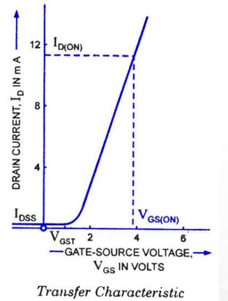
Is this Transfer Characteristic of a NMOS or PMOS device? How can you tell?
NMOS; VGS is positive (which will allow the electrons to flow through)
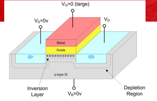
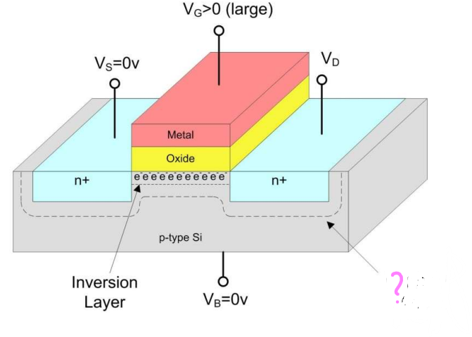
Label the following and explained how the layer is formed
Inversion Layer
as the gate-source voltage gets larger,
it attracts the minority carriers in the substrate to the oxide-Si surface and forms an inversion layer under the Gate oxide, which creates a channel between the Source and Drain
(when the surface potential (voltage) of the gate reaches the bulk Fermi potential (when the electric field becomes strong enough), the surface inversion will be established and an n-channel will form between the Source and Drain)
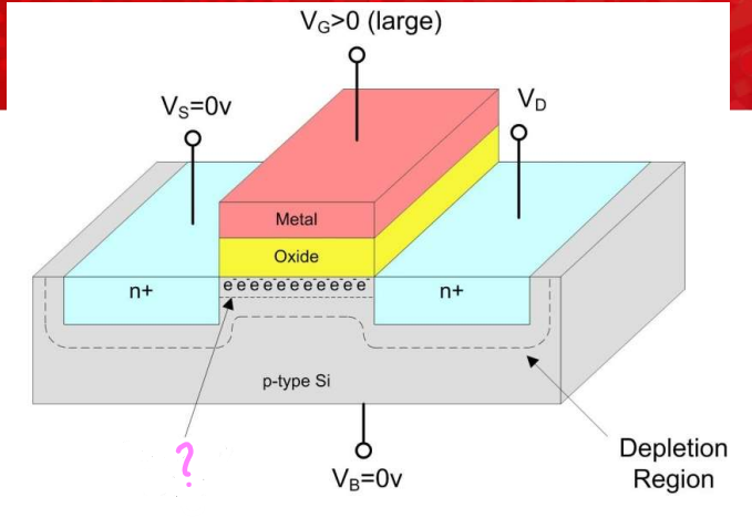
Label the mission region and briefly explain
Depletion Region
insulating region where no mobile charge carriers are present (mobile charge carriers have diffused away or forced away by an electric field SO there is nothing to carry a current here)
define doping
ion implantation
If I dope a substrate with boron, is the device NMOS or PMOS?
Boron is a p-type dopant (and it’s in the SUBSTRATE); therefore NMOS
Name the 3 components for micro and nano-fabrication
Thin film deposition (additive)
Lithography (lateral patterning)
Etching (subtractive)
(general process of adding then subtracting)
Fill in the stages of the microelectronics technology process
Starting wafer
Grow oxide
Depositor resistor material
Pattern resistor material
Deposit insulator
Pattern insulator
Deposit metal
Pattern metal

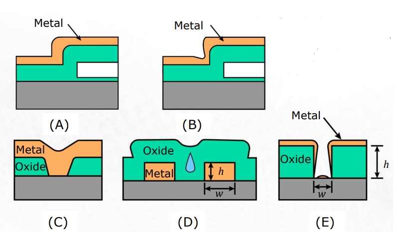
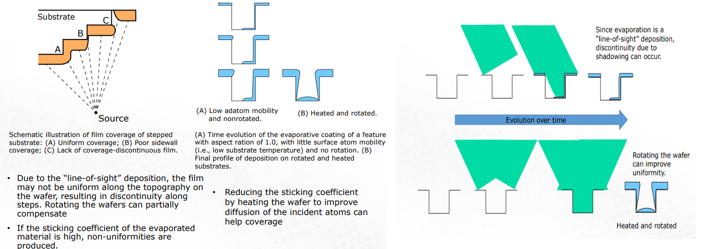
Categorize each example of thin film coverage or filling as good or problematic (if problematic, state why)
A) Good (Conformal step coverage with constant thickness on horizontal and vertical surfaces)
B) Problematic (poor step coverage; the thinner areas can heat up faster and cause cracking)
C) Good (good metal filling of a via or contact hole in a dielectric layer)
D) Problematic (shows poor dielectric filling between the metal lines, which leads to void formation- can trap moisture)
E) Problematic (poor filling of the bottom of a via hole with a barrier or contact metal)
Define Aspect Ration (AR)
h/W; ratio between height of the feature to width of the feature
(high AR = long and narrow, low AR = short and wide)
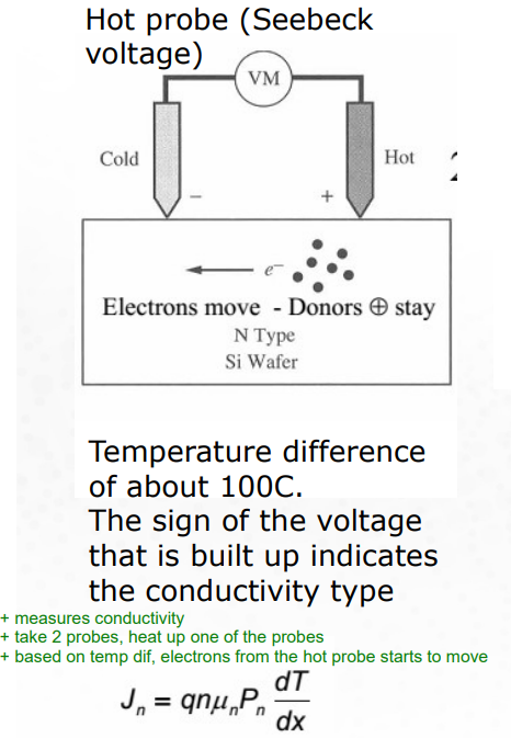
Explain the wafer/thin film characterization technique of Hot probe
[what it measures]
[how it measures it]
[what this measurement indicates]
Seebeck voltage (voltage difference generated in a material when there is a temperature difference between two points - directly related to the type of charge carriers (electrons or holes) that dominate in the material)
Place 2 probes on the surface, heat one probe (heating causes charge carriers to move from hot side to cold - movement of charge carriers generates a voltage difference between the two probes)
type of electrical conductivity (n-type or p-type) in a semiconductor wafer or thin film
(positive voltage = p-type)
(negative voltage = n-type)
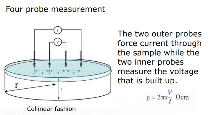
Explain the wafer/thin film characterization technique of the Four probe measurement
[what it measures]
[how it measures it]
[what this measurement indicates]
Voltage (The inner two probes measure the voltage drop that occurs due to this current. Because the inner probes do not carry the current, they measure only the potential difference - Compensates for contact resistance)
Four (evenly spaced) probes placed in contact with the surface of the material. The two outer probes force current through the sample, while the two inner probes measure the built up voltage.
Electrical Resistivity (intrinsic material property - how strongly a material opposes the flow of electric current)
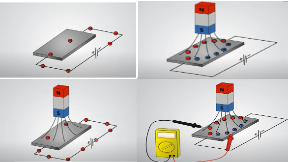
Explain the wafer/thin film characterization technique of the Hall Effect measurement
[what it measures]
[how it measures it]
[what this measurement indicates]
Hall Voltage (voltage that develops across a material when an electric current flows through it in the presence of a magnetic field)
Thin film placed in magnetic field perpendicular to its surface. Current is passed through the sample in a direction perpendicular to the magnetic field. Hall voltage measured used voltmeter
Number of carriers and mobility/speed of carriers (determines conductivity - how easily charge carriers can move through a material when an electric field is applied)
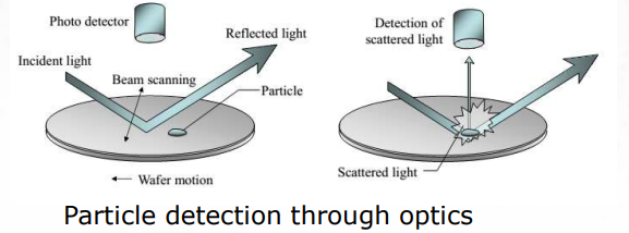
Explain the wafer/thin film characterization technique of the Particle Detection via Photo detector
light shines on wafer
particle scatters light
detector senses light scattered and alerts of a particle
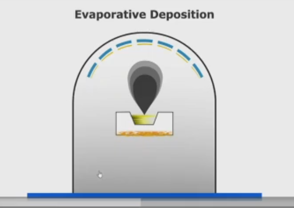
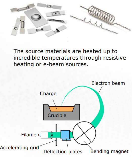
Explain the basic steps of the physical vapour deposition technique of Evaporation
Pump chamber to very low pressure (evacuate)
Heat (using current - resistive heating) the crucible containing charge (material you want to deposit) until it forms a vapour
Vapour “condenses“ on wafer forming the film
What is one major problem with the physical deposition technique of evaporation?
Inconsistent Coating (biased towards the forward direction; thicker film in the front than on the side)
Why can’t you have a completely homogenous thin film of an alloy formed through evaporation?
Metals have unique evaporation temperatures
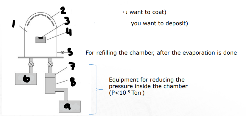
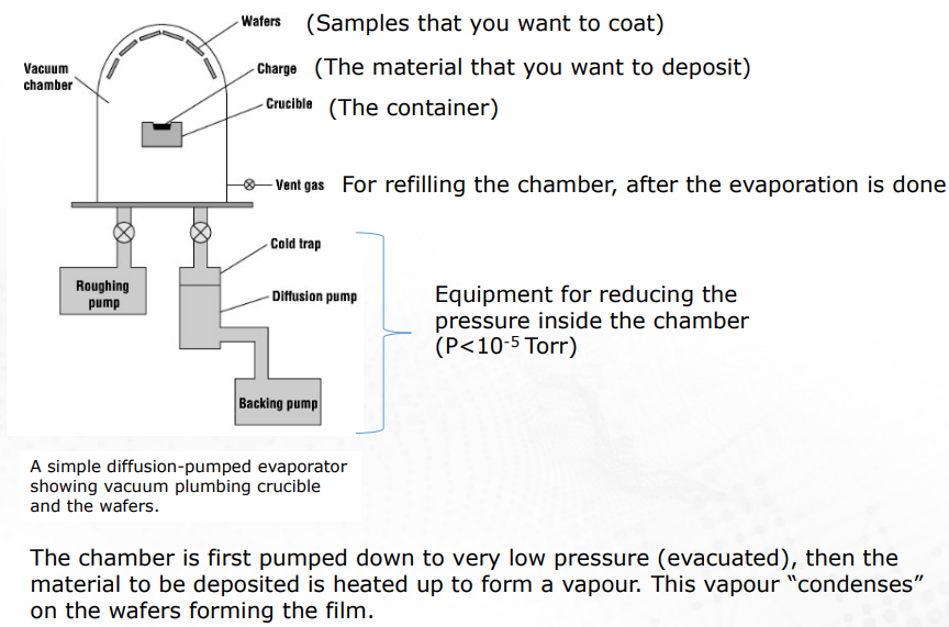
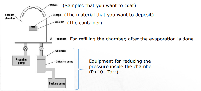
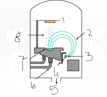
Label the basic components of the simple diffusion-pumped evaporator
Vacuum chamber
Wafers (Samples that you want to coat)
Charge (The material that you want to deposit, evaporant)
Crucible (the container of the charge)
Vent gas (For refilling the chamber, after evaporation)
Roughing pump (For lowering pressure)
Cold trap (For lowering pressure)
Diffusion pump (For lowering pressure)
Backing pump (For lowering pressure)
What happens when a negative photoresist is exposed to light?
light causes crosslinking → less soluble
(When exposed to light, the exposed areas of a negative photoresist become less soluble in the developer. This happens because the light causes a chemical reaction that cross-links the polymer chains, making the exposed areas harder to dissolve. Therefore, the unexposed areas are removed during development.)
What happens when a positive photoresist is exposed to light?
light breaks polymer chains of photoresist → more soluble
(When exposed to light, the exposed areas of a positive photoresist become more soluble in the developer. This is because the light breaks down the polymer chains, making the exposed areas easier to dissolve. As a result, the exposed areas are removed during development.)
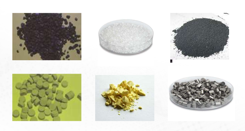
Which of the following materials can be used in evaporation deposition?
Metallic chunks
Powders
Ceramics
All of the above
Primary difference between resistive evaporation and electron beam evaporation (method of heating)
resistive: current is passed through crucible
electron beam: electron beam applied to target directly
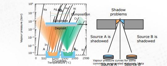
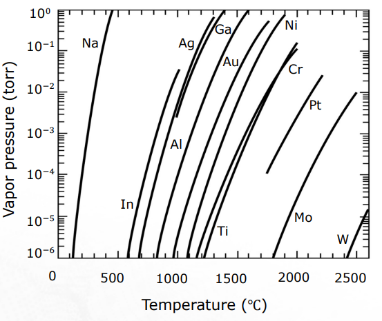
Define vapor pressure
indication of how much of a material is evaporating
(to obtain reasonable deposition rates, a vapour pressure of 10 millitorr is recommended - Vapour pressure curves for some commonly evaporated materials from Alcock et al
graph implication: hard to form alloy thin film)
Define a dielectric material
an insulator that, when exposed to an electric field, can be polarized
(dielectrics are insulating materials that can be polarized, meaning their positive and negative charges can be slightly separated when an electric field is applied. This property makes them useful in devices like capacitors, where they help store and release electrical energy efficiently. Common examples of dielectric materials include rubber, glass, plastic, and ceramics)
True or False:
During e-beam evaporation, the e-beam only hits the target; therefore, in general, e-beam evaporation is cleaner (creates a purer film) than thermal evaporation because the crucible is not heated up (therefore, isn’t degrading/no dirt from the crucible is coming off)
True
True or False:
e-beam evaporation can reach a wider (higher) range of temperatures than thermal evaporation
True
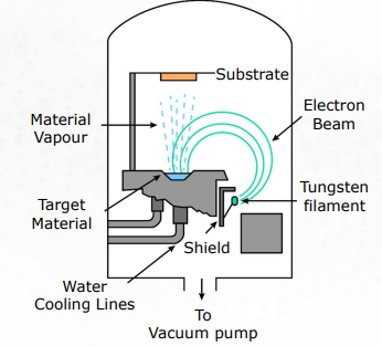
Label the following diagram for e-beam evaporation
Substrate
Electron beam
Tungsten filament
Sheild
Space to pump
Water cooling lines
Target Material
Material Vapour
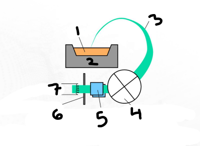
Label the following diagram for e-beam evaporation
Charge (material in the crucible)
Crucible
Electron beam
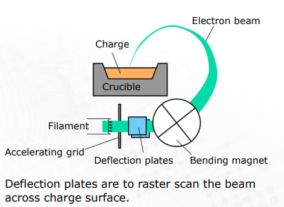
Bending magnet (focus beam/bend and direct the accelerated electron beam towards the charge in the crucible)
Deflection plates (to raster scan the beam across charge surface)
Acceleration grid (accelerate the electrons emitted by the filament towards the material in the crucible. The electrons gain kinetic energy as they are accelerated, which allows them to effectively transfer energy to the charge material upon impact, leading to evaporation)
Filament (wire heated by passing electric current through it; emits electrons)
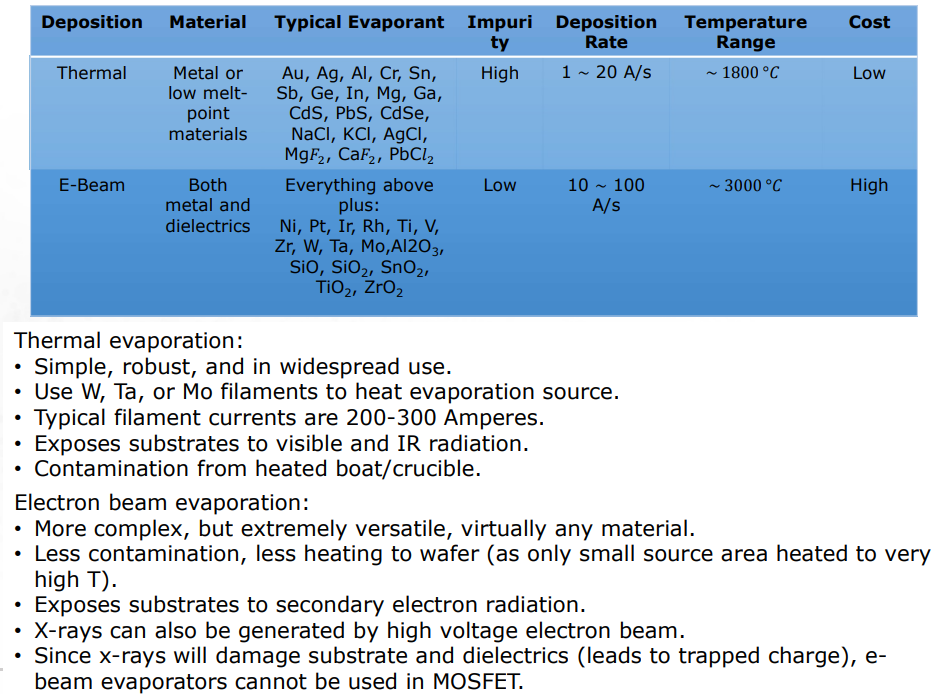
Fill in the following information for Thermal vs. E-beam evaporation
Format of answers: Thermal, E-beam
1. Material
2. Impurity
3. Deposition Rate
4. Temperature
5. Cost
6. Radiation
1. Metal or low melting-point materials, Both metal and dielectrics
2. High, Low
3. 1-20 A/s; 10-100 A/s (angstroms per second (Å/s))
4. 1800 C, 3000 C
5. Low, High
6. Visible and IR, secondary electron and x-ray
During evaporative deposition, why does the substrate need to be heated as well as the source?
Desorption of impurity atoms on the surface of the substrate
Why do you want low background pressure (vacuum) for in the evaporative deposition chamber?
Prevent contamination (Remove particles/unwanted gas atoms from the path the source material is going to travel to reach the substrate)
What changes when the source temperature is increased in evaporative deposition?
More atoms are released → thicker film (NOTE: the speed at which the atoms are travelling does NOT change - the atoms do NOT have more energy)
Does a higher substrate temperature (for evaporative deposition) lead to thin film with larger grains or smaller grains?
Larger grains (lower nucleation rate because the adatoms have sufficient energy to diffuse across the surface instead of immediately forming new nucleation sites. i.e. enhanced surface mobility promotes the growth of larger grains, as adatoms can more easily find their way to the growing edges of existing grains, thereby facilitating grain coarsening)
What happens when you move the substrate closer to the source during evaporative deposition?
What problem can this cause?
film becomes thicker faster (source atoms are evaporating in all directions; bringing the substrate closer means that it will pick up some of the atoms that would otherwise not make it to the substrate if the substrate was further away)
higher non-uniformity
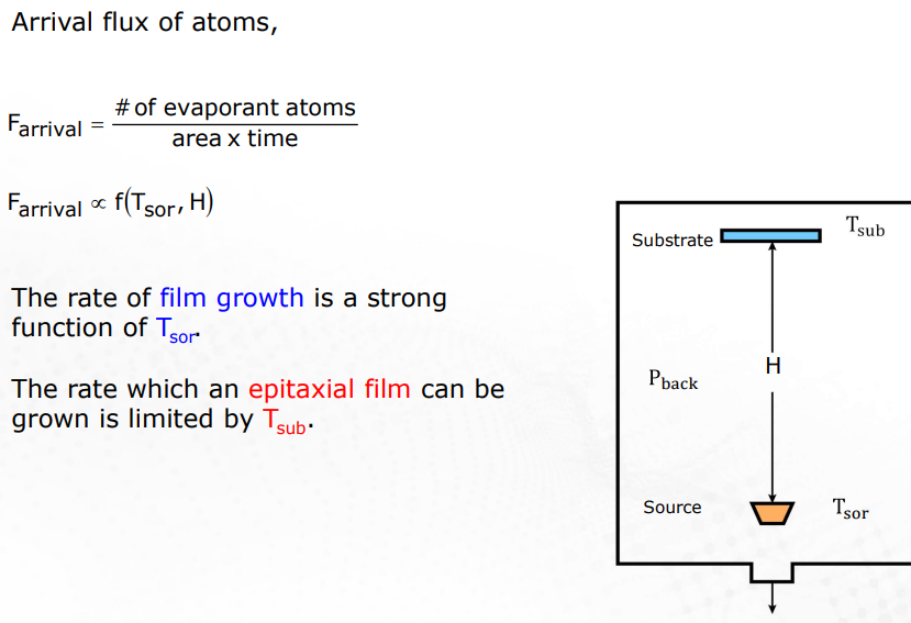
Fill in the blank: The rate of film growth is a strong function of [BLANK]
Source temperature (higher temp → more source atoms evaporated)
Fill in the blank: The rate which an epitaxial film (thin layer of crystalline material that is deposited onto a crystalline substrate) can be grown is limited by [BLANK]
substrate temperature (controls surface mobility of adatoms, which controls how the adatoms organize themselves on the substrate)
In the context of evaporative deposition, define arrival flux
number of atoms or molecules arriving per unit area of the substrate per unit time (which is inversely proportional to H - hearth design/distance between substrate and source)
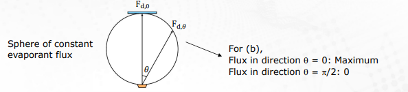
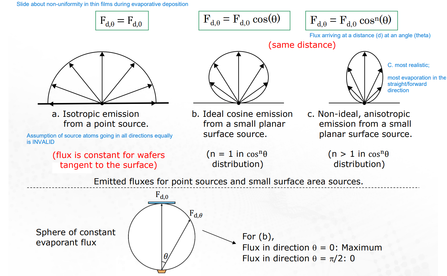
For what theta is the deposition flux at a maximum?
0 (zero)

For what theta is the deposition flux at a minimum (zero)?
pi/2
What is the advantage of keeping the wafer further away during evaporative deposition?
more uniform (less theta variation - flux variation decreases- REMEMBER: NOT a point source; reality: AREA SURFACE SOURCE)
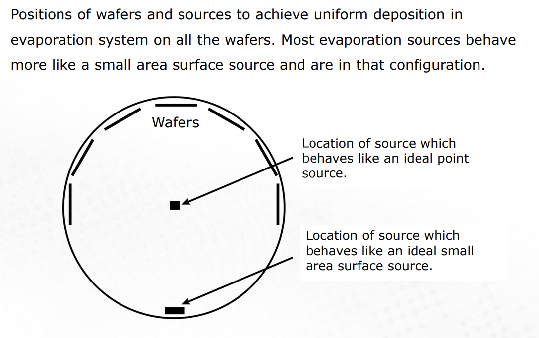
Which direction does evaporative deposition favor?
Forward/straight direction
List a few disadvantages of evaporative depostion
Difficult to get thickness uniformity over large wafers
Difficult to evaporate high melting point sources
Evaporating alloys is extremely challenging
Low throughput (number of wafers you’re outputting) due to Ultra High Vacuum (UHV) - slow process
Poor step coverage (shadowing effect)
Challenging to evaporate compounds such as SiO2 (compounds breakdown - i.e. can end up with SiO1.8)
List a few advantages of evaporative deposition
Little damage to the wafer (no energetic particles - evaporated atoms are gently condensing onto the surface of the substrate)
Deposited films are usually very pure due to UHV
Electron-beam based probes are available for analysis of the surface structure during growth (because this process of deposition is slow)
What are some ways to overcome the issue of step coverage during evaporative deposition?
heat and rotate
What are 2 problems with alloy evaporation?
Compound material breaks down at high temperature
Each component in the alloy has different vapour pressure, therefore different deposition rate, resulting in a film with different stoichiometry compared to the source
What is one solution to the issue of alloy evaporation?
2 e-beam guns (alloy forms in the overlap of the deposition materials - but ratio will not be equal - dual shadow effect)