CSC258: Sequential Circuits
1/42
There's no tags or description
Looks like no tags are added yet.
Name | Mastery | Learn | Test | Matching | Spaced |
|---|
No study sessions yet.
43 Terms
sequential circuits
circuits that also depend on both the current inputs and the prev state of the circuit
what is a sequential circuit?
this creates circuits whose internal state can change over time, where the same input values can result in different outputs
why would we need sequential circuits?
for memory values and reacting to changing inputs
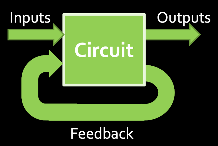
how to create sequential circuits?
essentially, sequential circuits are a result of having feedback in the circuit
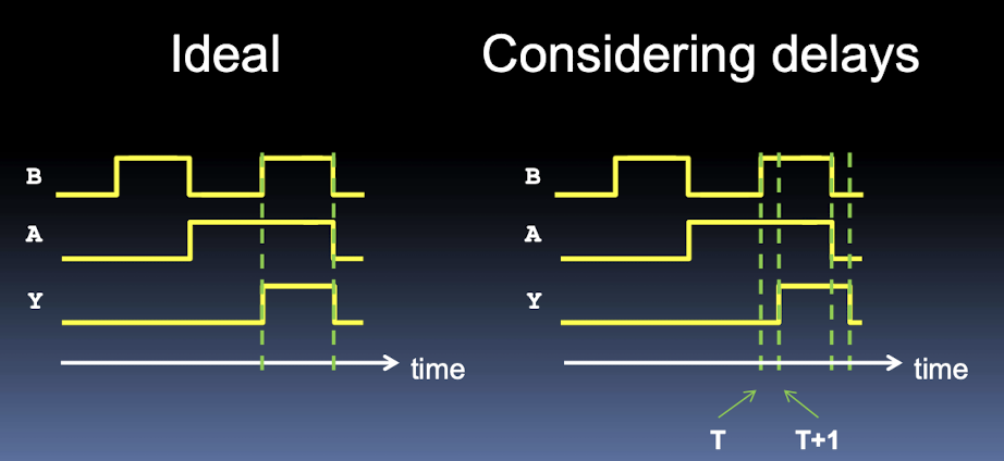
gate delay (propagation delay)
“the length of time it takes for an input change to result in the corresponding output change”
even in combinational circuits, outputs dont change instantaneously
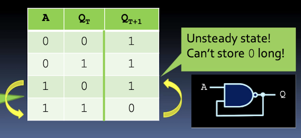
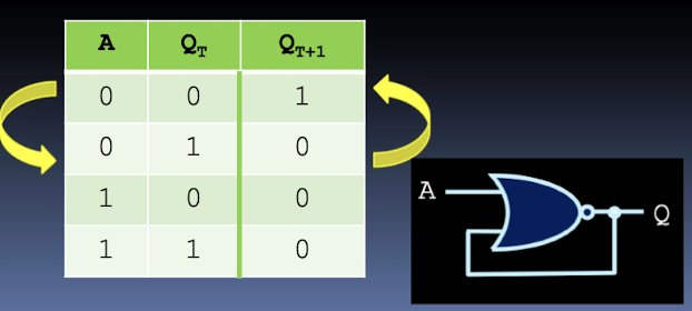
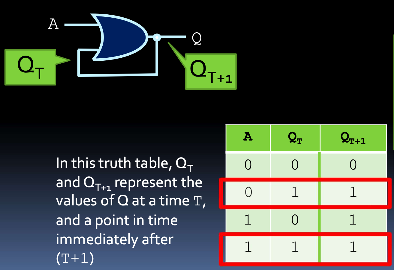
what makes NAND and NOR feedback circuits different than AND and OR?
unlike the AND and OR gate circuits (which get stuck), the output QT+1 can be changed, based on A
NAND feedback example
lets assume we set A=0, then output Q will go to 1, so if we leave A unchanged we can store 1 indefinitely.
but if we set A=1, Q’s value can change but it is unsteady and will oscillate between 0 and 1
NOR feedback example
lets assume we set A=1, then output Q will go to 0, if we leave A unchanged we can store 0 indefinitely.
if we set A=0 then Q’s value can change but it is unsteady and will oscillate between 0 and 1
feedback behaviour of NAND and NOR
output QT+1 can be changed based on A, however gates that feed back on themselves could enter an unsteady state
latches
if multiple gates that feed back on themselves are combined, you can get more steady behaviour
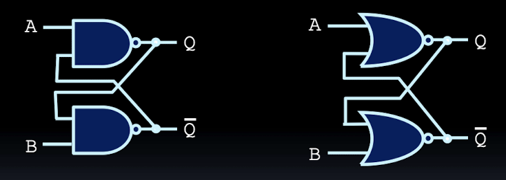
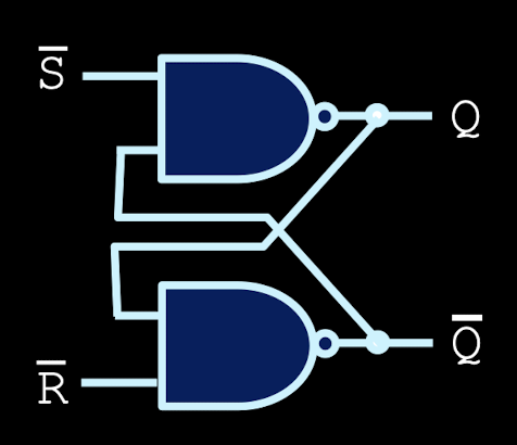
SR latch
A memory circuit with two inputs, S (Set) and R (Reset), and two outputs, Q and Q’. The Set input stores a logic high, and the Reset input clears it to logic low. Going from 11 to 00 produces unstable, output depends on which input changes first.
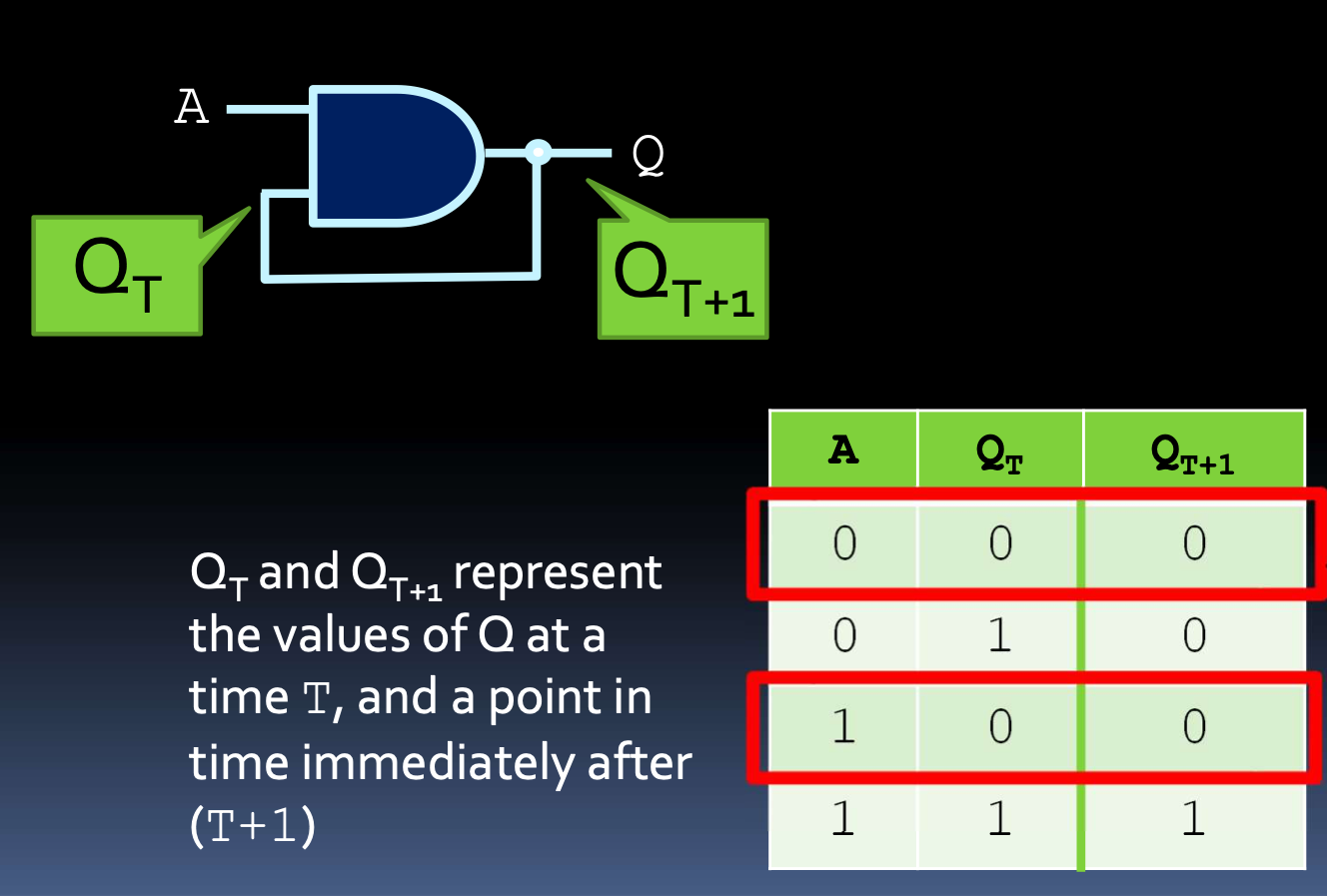
AND feedback example
if A=0, QT+1 becomes 0 no matter what QT was, so QT+1 gets stuck at 0 and cannot change
OR feedback example
if A=1, QT+1 becomes 1 no matter what QT was, so QT+1 gets stuck at 1 and cannot change
What is the difference between a latch and a flip-flop?
Latches are level-triggered, meaning they respond to input changes as long as the enable signal (control) is active. Flip-flops are edge-triggered and only respond at the rising or falling edge of a clock signal.
more on instability
unstable behaviour occurs when a S’R’ latches inputs go from 00 to 11 or when a SR latches inputs go from 11 to 00, things dont change simultanouly so the outcome depends on which signal changes first
because of the forbidden state, 00 is considered a forbidden state in NAND based S’R’ latches, and 11 is considered a forbidden state in NOR based SR latches
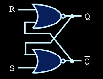
S’R’ latch
is a variation of the SR latch, where the Set (S) and Reset (R) inputs are inverted. This means that a low (0) signal on S' sets the latch (Q = 1), and a low (0) signal on R' resets the latch (Q = 0). When both inputs are high (1), the output holds its previous state. Going from 00 to 11 produces unstable behaviour because output depends on which input changes first.
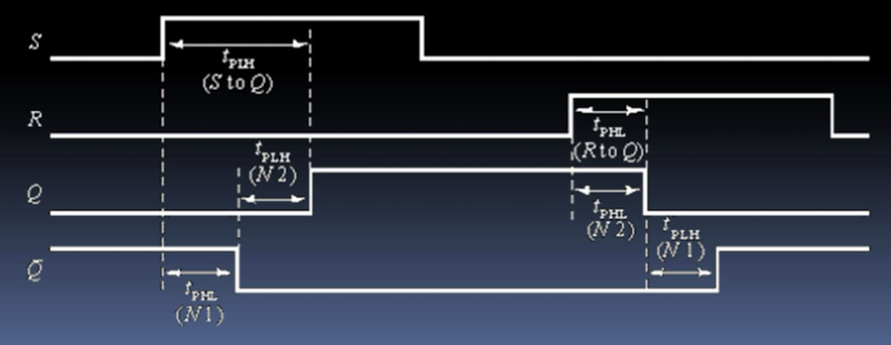
SR latch timing diagram
important to note that the output signals dont change instantaneously
clock signals
“clocks” are a regular pulse signal where the high value indicates when to update the output of the latch, faster clock signal —> more executions
frequency
how many pulses occur per second, measured in Hertz
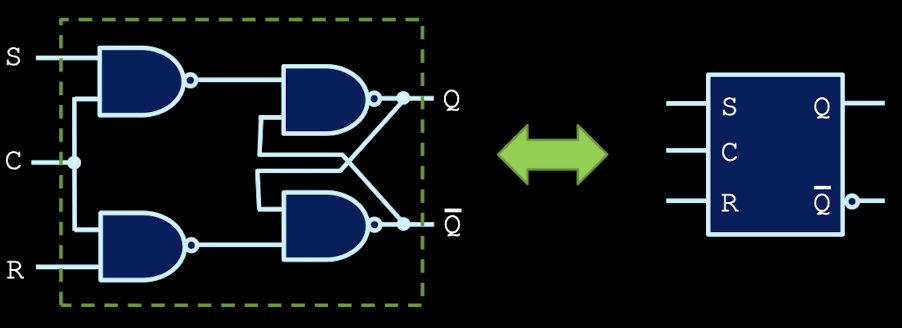
clocked SR latch
adding another layer of NAND gates to the S’R’ latch gives us this, and adds more control
if clock is high, the first NAND gates invert those values, which get inverted again in the output, setting both inputs to 0 maintains the output values
the clock needs to be high in order for the inputs to have any effect
is there a forbidden state for clocked SR latch?
yes, assuming the clock is 1, when both S and R are 1 it becomes a forbidden state. it is forbidden because both Q and Q’ would be high which contradicts their inverse nature.
is there a solution to the forbidden state in clocked SR latch?
yes! prevent S and R from having high values at the same time, eg a D latch
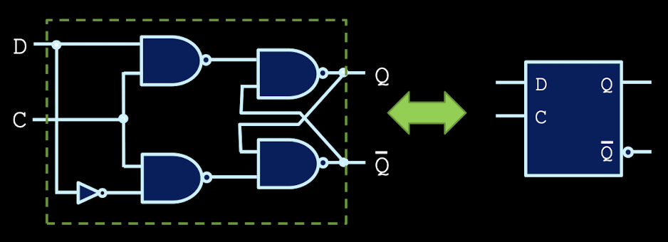
what is a D latch?
D replaces S and R from the gated SR latch so you avoid the indeterminate state problem. the value of D now sets output Q low or high whenever C is high. eg light switch. issue: timing
what does latches are transparent mean?
the output of a latch should not be applied direclty or through combinational logic to the input of the dame or another latch when they all have the same clock signal
transparent means
any changes to the inputs of a D latch are visible to the output when clock is 1
value triggered
values can change as long as the clock is high
edge triggered
values can only change once per clock change
solution to latch timing issues
create a middle section that is set to the input value when clock is high, and then sends that value to the output when the clock is low
flip flop
latched circuit whose output is triggered with the rising edge or falling edge of a clock pulse
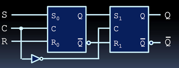
SR flip flop
Is a type of sequential logic circuit that has two inputs, S (Set) and R (Reset), and two outputs, Q and Q’. It is edge-triggered, meaning it captures and stores the input values on a specific edge (rising or falling) of a clock signal. The SR Flip-Flop can set, reset, or maintain its state based on the inputs and the clock, making it useful for storing binary information.
Still have issues with unstable behaviour
D flip flop
solution to SR flip flop unstability
negative edge triggered, connect D latch to input of SR latch
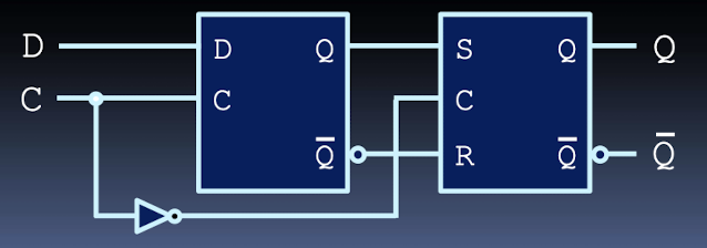
behaviour of D flip flop
if the clock signal is high, the input to the first flip flop is sent out to the second
the flip flop doesnt do anything until the clock signal goes down again
when the clock goes from high to low, the first flip flop stops transmitting a signal and the second one starts
if the input to D changes, the change isnt transmitted to the second flip flop until the clock goes high again
once the clock goes high, the first flip flop starts transmitting at the same time as the second flip flop stops
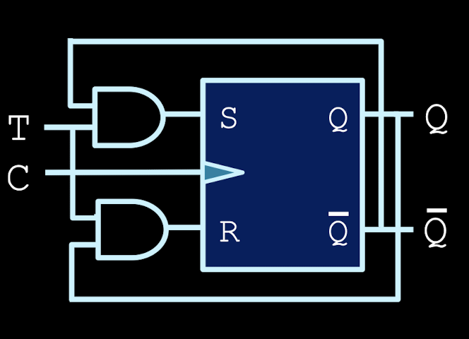
T flip flop
similar to the D flip flop except the clock makes it toggle (flip between 0 and 1) whenever the T input is high
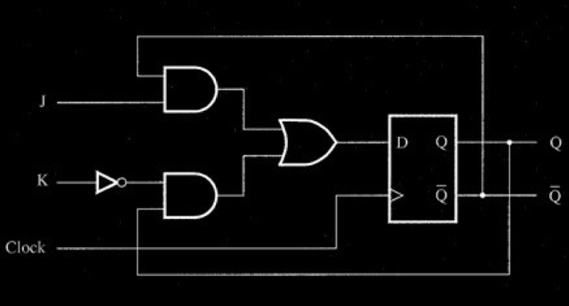
JK flip flop
takes advantage of all combos of the two inputs to produce 4 different behaviours
J | K | Behaviour |
0 | 0 | maintain output |
0 | 1 | reset output to 0 |
1 | 0 | set output to 1 |
1 | 1 | toggle output value |
flip flop timing
input should NOT be changing at the same time as the active edge of the clocks
setup time
input should be stable for some time before active clock edge
hold time
input should be stable for some time immediately after the clock edge
maximum clock frequency
time period between two active clock edges cannot be shorter than longest propagation delay between any 2 flip flops + setup time of the flip flop
resetting inputs
since flip flops have unknown state when they are first powered up, we need a convenient way to initialize them
reset signal resets the flip flops output to 0
synchronous reset
the output is reset to 0 only on the active edge of the clock
asynchronous reset
the output is reset to 0 immediately (as soon as the asynchronous reset signal becomes active), independent of the clock signal
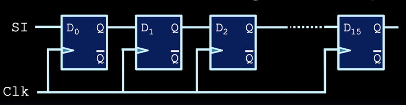
shift registers
a series of D flip flops can store a multi-bit value (such as a 16-bit integer, for example)
data can be shifted into this register one bit at a time, over 16 clock cycles
load registers
one can load a register’s values all at once, by feeding signals into each flip flop
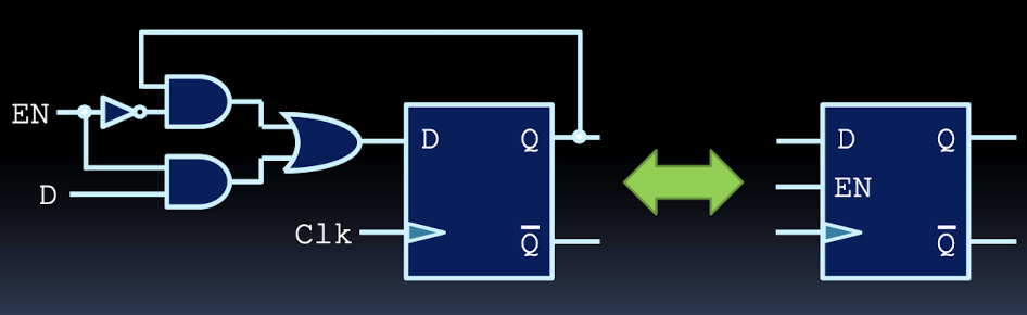
to control when this register is allowed to load its values, we introduce the D flip flop with enable