Semiconductors
1/23
There's no tags or description
Looks like no tags are added yet.
Name | Mastery | Learn | Test | Matching | Spaced | Call with Kai |
|---|
No analytics yet
Send a link to your students to track their progress
24 Terms
Semiconductor
A material whose resistance is between that of a good conductor and a good insulator.
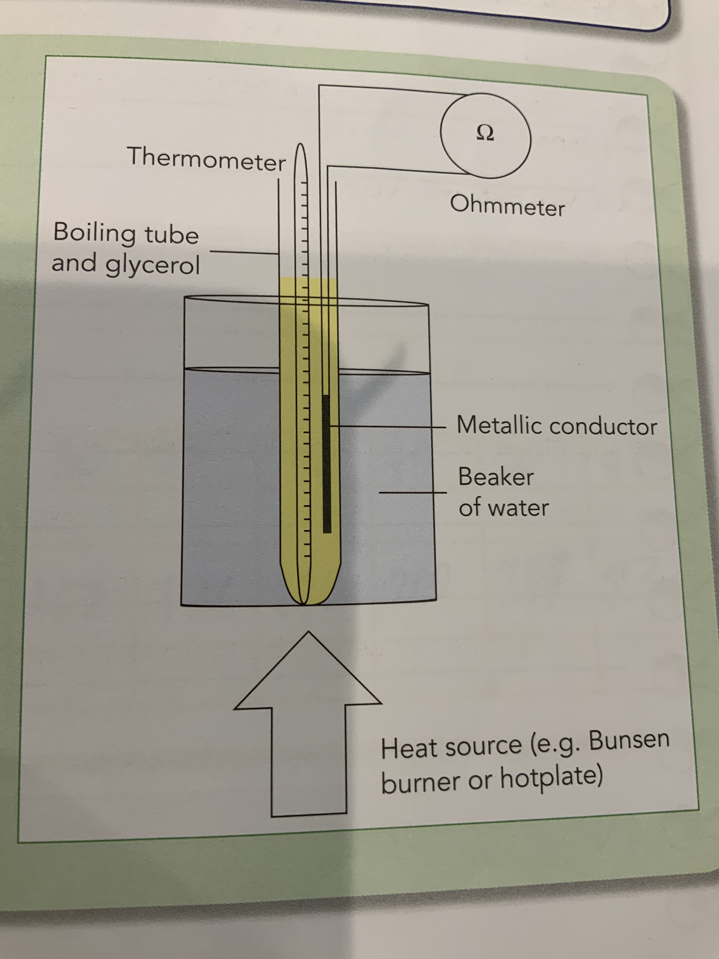
Relationship between temperature and resistance of a semiconductor
Resistance decreases as temperature increases
Intrinsic Conduction
The movement of charges through a pure semiconductor due to electrons moving from negative to positive and an equal number of holes moving in the opposite direction.
OR
The movement of charges through a pure semiconductor due to the creation of “electron-hole pairs”
Thermistor
An electrical component whose resistance decreases rapidly with increasing temperature.
Doping
Adding a controlled amount of an impurity to a pure semiconductor to increase its conductivity.
Extrinsic Conduction
The movement of charges through a doped semiconductor
n-type semiconductor
Semiconductor in which electrons are the majority of charge carriers.
How is an n-type semiconductor produced?
Doping a pure semiconductor with phosphorus
p-type semiconductor
A semiconductor in which holes are the majority of charge carriers.
How is a p-type semiconductor produced?
Doping a pure semiconductor with boron
Explain how adding phosphorous or boron increases conductivity of a conductor.
Phosphorus increases conductivity by adding more charge carriers in the form of electrons. Boron increases Conductivity by adding more charge carriers in the form of holes
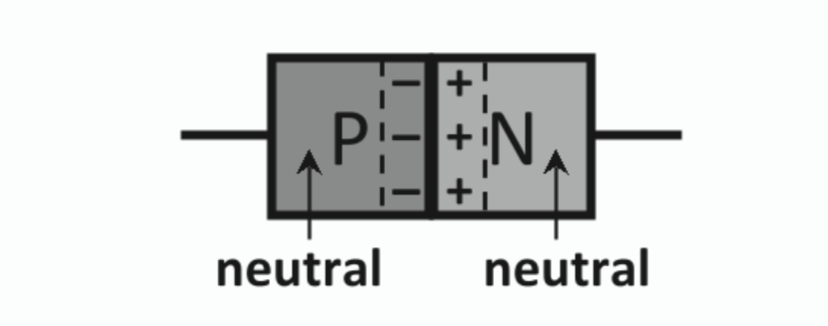
The p-n junction
When a piece of p-type semiconductor is joined to a piece of n-type semiconductor, the junction between them is known as the p-n junction.
Depletion Layer
Region at both sides of a p-n junction that contains no free majority charge carriers.
How is a depletion layer formed?
When a p-type material is placed against an n-type material:
Free electrons from the n-type move towards the p-type and find holes to become stable.
Holes move from the p-type into the n-type and find electrons to become stable.
This causes a region to form around the junction containing virtually no charge carriers - the depletion layer.
Forward biased p-n junction
To connect a p-n diode in forward bias, connect the positive terminal to the p-type and negative terminal to the n-type.
The positive terminal pushes holes in the p-type material toward the depletion layer.
The negative terminal pushes electrons in the n-type material toward the depletion layer.
This eventually eliminates the layer and current flows. When an external voltage overcomes the junction voltage.
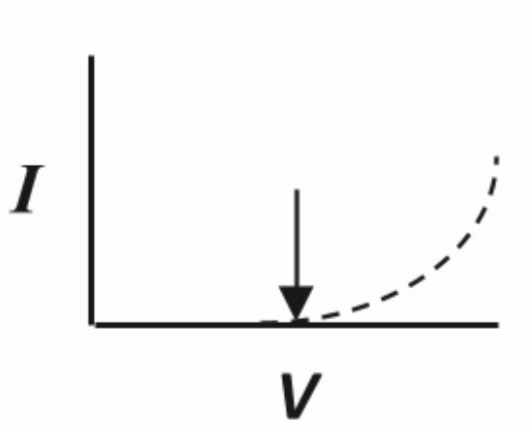
Reversed-biased p-n junction
Connect the positive terminal to the n-type and negative terminal to the p-type.
The diode will not conduct and the depletion layer widens.
The end result is that no charges actually move through the depletion region and it remains an insulator.
In this instance reverse current can be detected with a micro ammeter.
Describe how a junction voltage is produced at the p-n junction?
A junction voltage is the electric voltage that forms across a p-n junction because electrons and holes move and create an electric field when the materials are joined.
Indicate on a diagram, the area of a p-n junction that are positively charged, negatively charged, and neutral.
Sketch a graph to show the variation of current with voltage for a reverse biased semiconductor circuit. Label the junction voltage on your graph.
How does a diode act as a rectifier?
A diode acts as a rectifier by allowing current to flow in only one direction, converting AC to DC.
What is the function of a rectifier?
Converting A.C to D.C
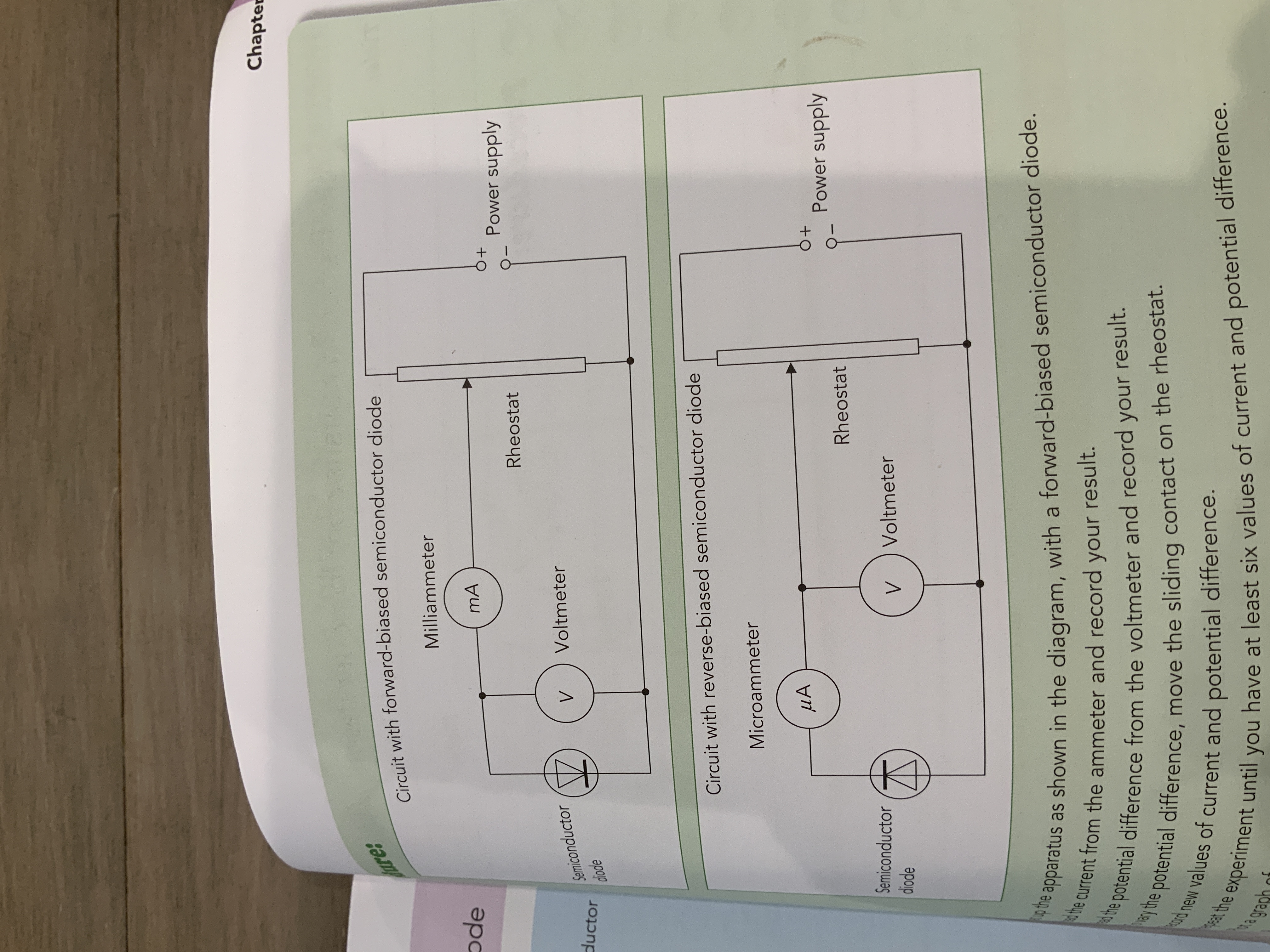
Mandatory experiment of the variation of current with potential difference for a semiconductor diagrams.
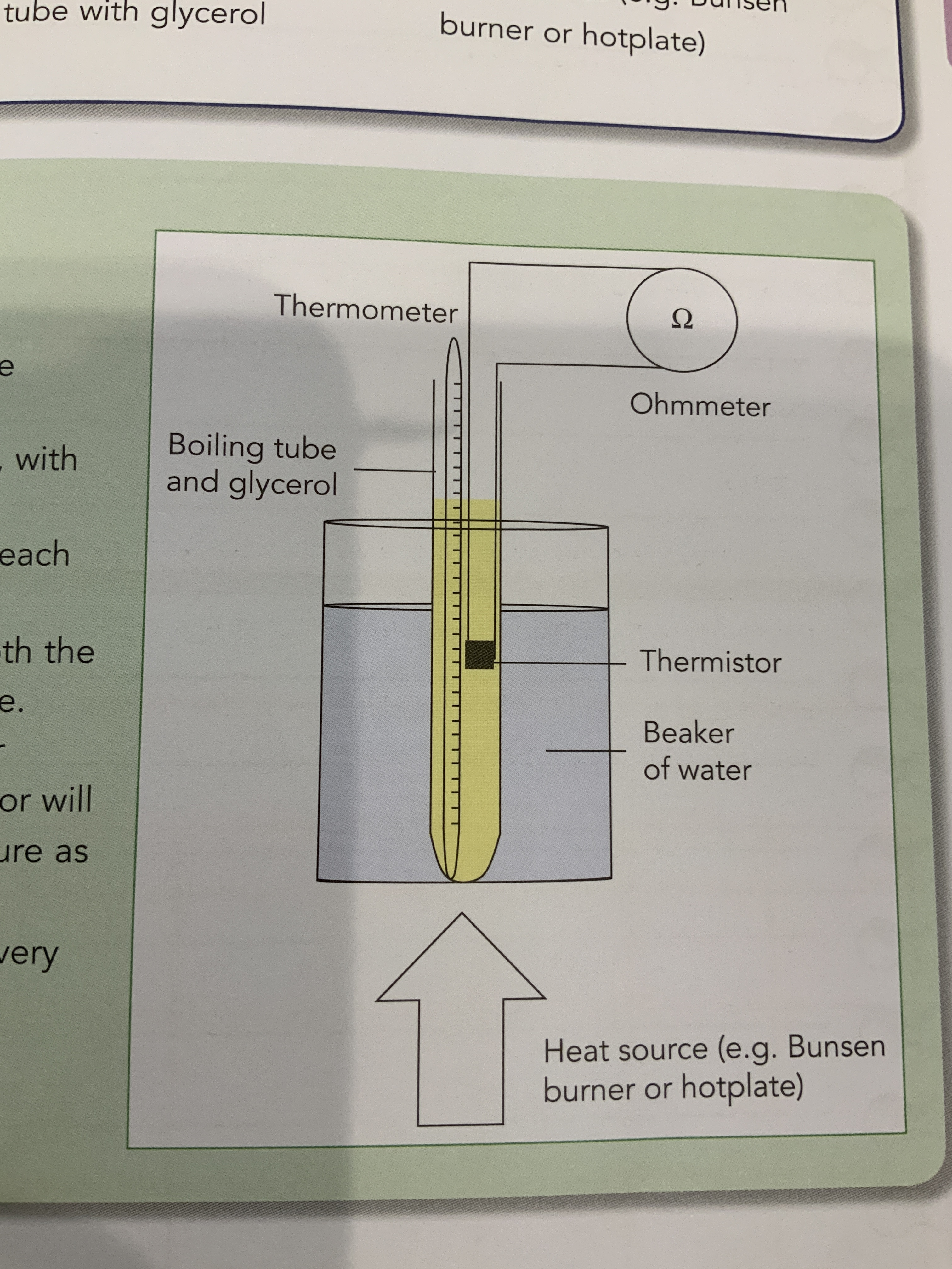
Mandatory experiment of variation of temperature and resistance of a thermistor diagram.
Mandatory experiment of variation of temperature and resistance of a conductor diagram.