Electron Microscopy
1/29
There's no tags or description
Looks like no tags are added yet.
Name | Mastery | Learn | Test | Matching | Spaced | Call with Kai |
|---|
No analytics yet
Send a link to your students to track their progress
30 Terms
Electron probe
Electrons can be accelerated by electrical potential decreasing their wavelength
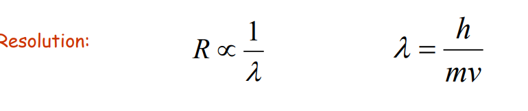
Wavelength of electron
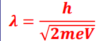
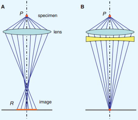
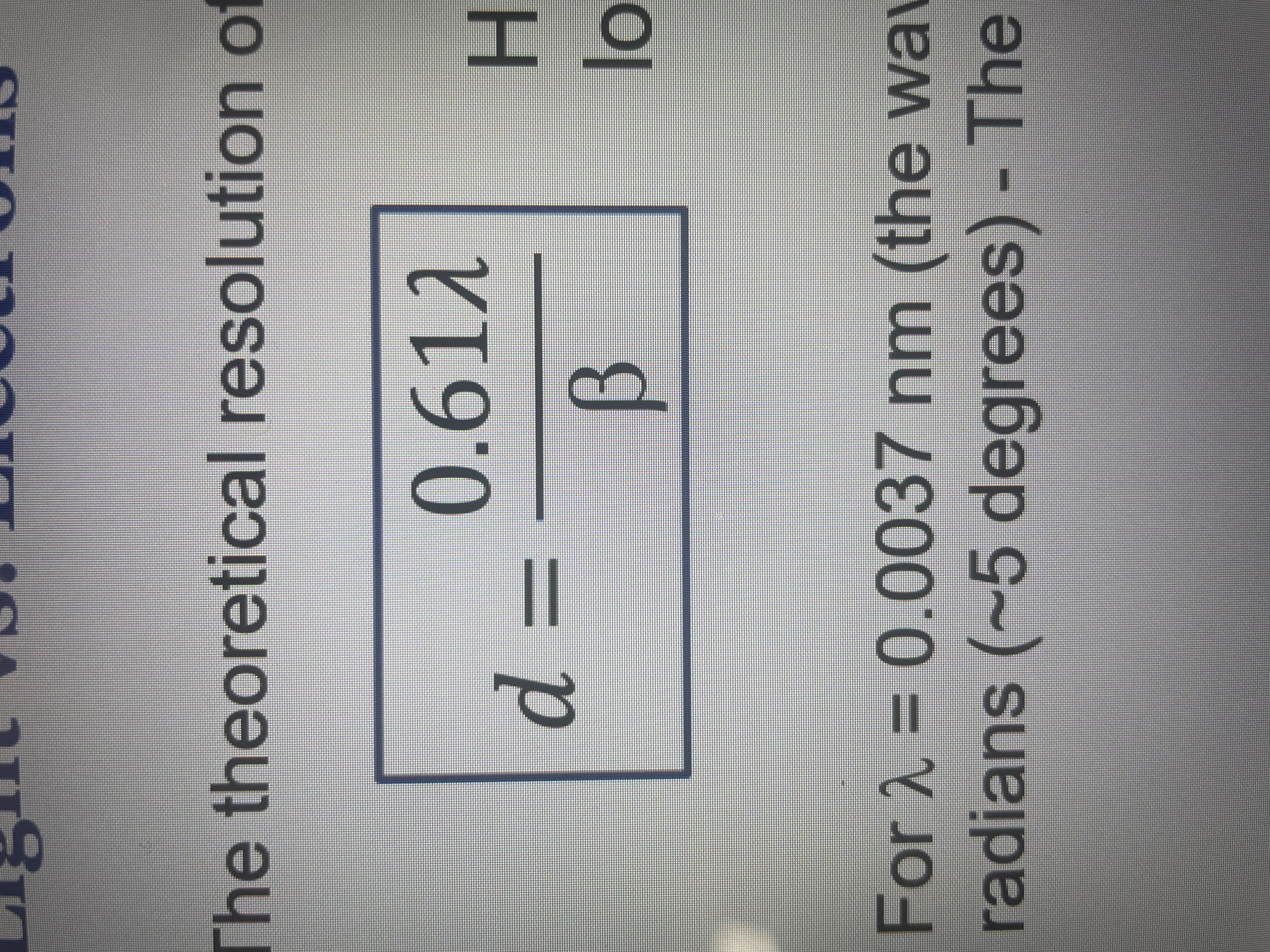
Resolution
Scanning Electron microscopy
Produces images of a sample by scanning it with a focused beam of electrons
Microscope Applications:
▪ Topography (texture/surface of a sample)
▪ Morphology (size/shape of particles)
▪ Composition (elemental composition of sample
▪ Crystallographic information (arrangement present within sample)
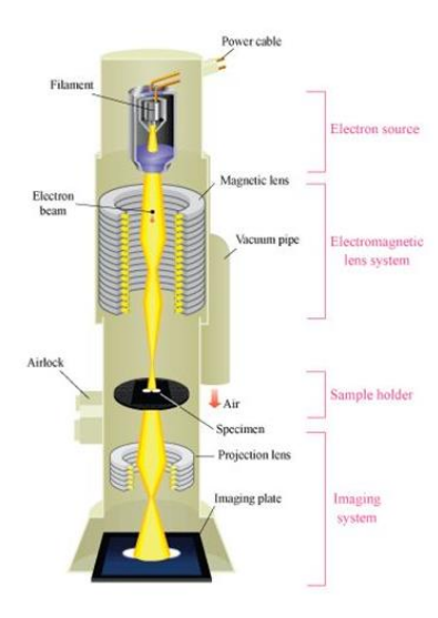
Instrumentation
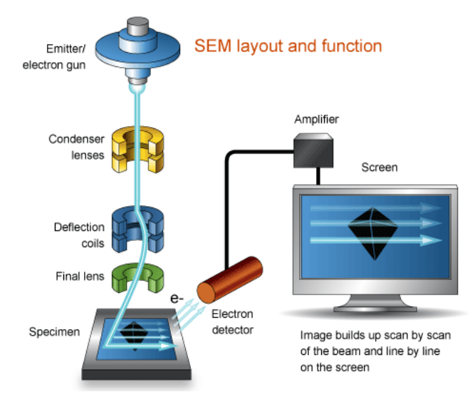
Electron Beam Generation
Electron gun – generates a beam of electrons and accelerates them to energies in the range
Thermoionic gun
Field emission gun (FEG)
Electromagnetic Lenses
The purpose of a lens is to change the path of the rays in a desired direction.
The deflection experienced by a charged particle in a magnetic field is given by the Lorentz force law.
Condenser lens: adjust diameter of electron beam
Objective lens: Focuses the beam onto the sample
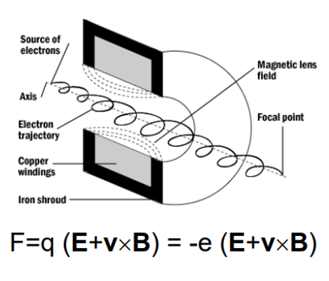
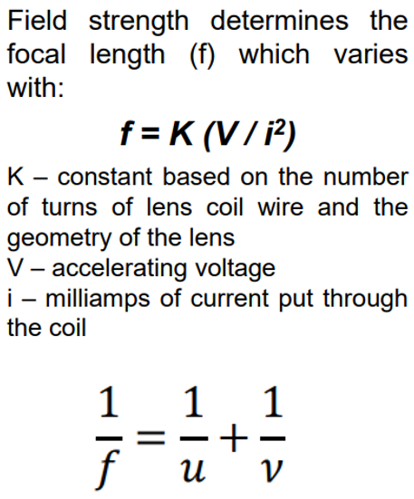
Electromagnetic Lenses: Focal length
The focal plane of the lens is the plane in which the parallel rays are brought to a focus.
Vacuum
It minimises scattering of the electron beam before reaching the specimen
Scattering or attenuation of the electron beam will increase the probe size and reduce resolution
Electron–Matter Interactions
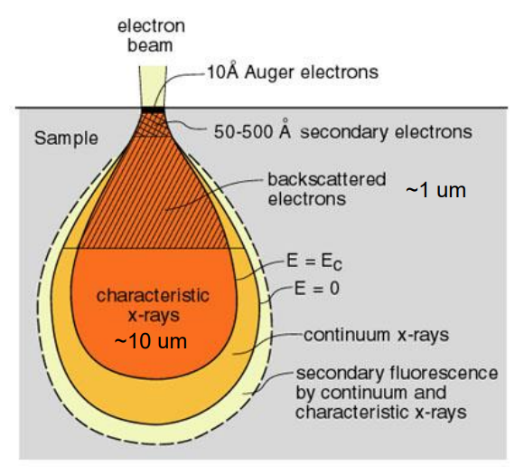
Interactions: Auger
Relaxation of electron ionized atoms lea to emission of Auger electrons
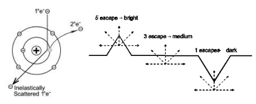
Interactions: Secondary Electrons
Caused by an incident electron whcih imparts some of it energy to a lower energy electron as kinetic energy ~ 5eV.
Can produce several secondary electrons
Topogical
Bumps: bright image
Indents: dark image
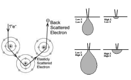
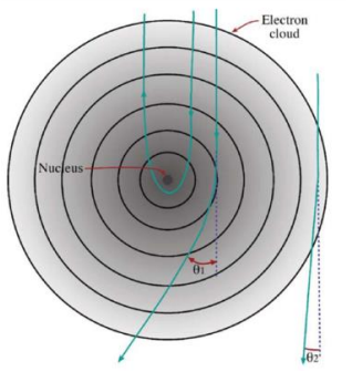
Interactions: Back scattered electrons
Caused when an incident electron collides with an atom normal to incident path, and is scattered backwards 180o.
High atomic number: bright
Low atomic number: dark
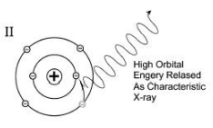
Interactions: X-rays
As the electron falls it emits energy, usally as x-rays to balance the total energy.
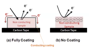
Charge Coating
For non conducting materials: coating layer grounds excess negative charge build-up.
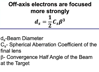
SEM Resolution: Spherical abberations
lens more powerful at edge then at the centre
Disc of minimum confusion (dmin) results instead of point focus
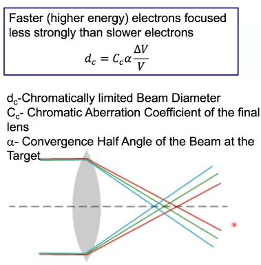
SEM Resolution: Chromic abberations
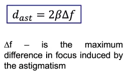
SEM Resolution: Astigmatism
Occurs when the electrons sense a non-uniform magnetic field as they spiral round the optic axis.
Transmission electron Microscopy
A beam of electrons is transmitted through an ultra-thin specimen, interacting with the specimen as it passes through it.
2D image
Interactions: Transmitted unscattered electrons
No interactions between electrons and sample (no deflection from the original path) as electrons transverse the specimen.
Thick specimin: dark (less transmitted)
Thin specimin: bright
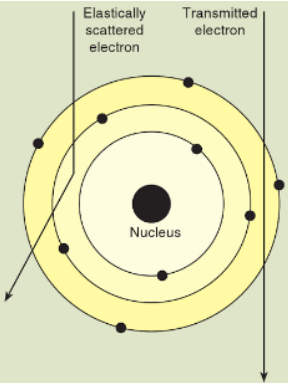
Interactions: Transmitted elastically scattered electrons
Incident electrons scattered by the atoms in the specimen in an elastic fashion (no loss of energy).
Crystalline materials coherent.
At higher angles elastic scattering becomes more incoherent.
Interactions: Inelastic Scattered Electrons
Electrons interact with the specimen atom in an inelastic fashion.
Large angles - incoherent
Amount of backscatter scales with thickness
Kakuchi Bands: alternating dark/light lines relating to atmonic spacing
Instrumentation
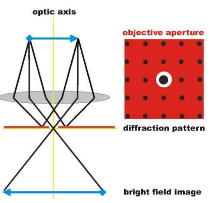
Bright Field Mode
When the aperture is positioned to pass only the transmitted (un-diffracted) electrons.
Image is bright where diffraction in specimin is weak.
Thick regions: dark
No sample: bright
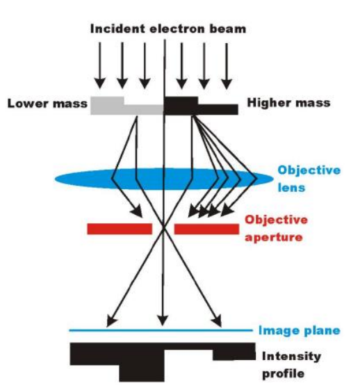
Mass Thickness Contrast
High-Z/Thicker specimins scatter more
Number of unscattered electrons decreases exponentially with thickness
Amorphous no diffraction
Density and thickness determine contrast
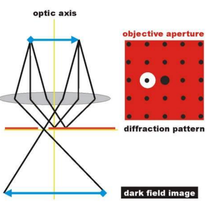
Dark Field Mode
When the aperture is positioned to pass only some diffracted electrons (exclude primary beam).
No scattering (primary beam): dark
study crystal defects
Diffraction Pattern
Fourier transform of the periodic crystal lattice, giving us information on the periodicities in the lattice and hence the atomic positions.
Information on crystallinity
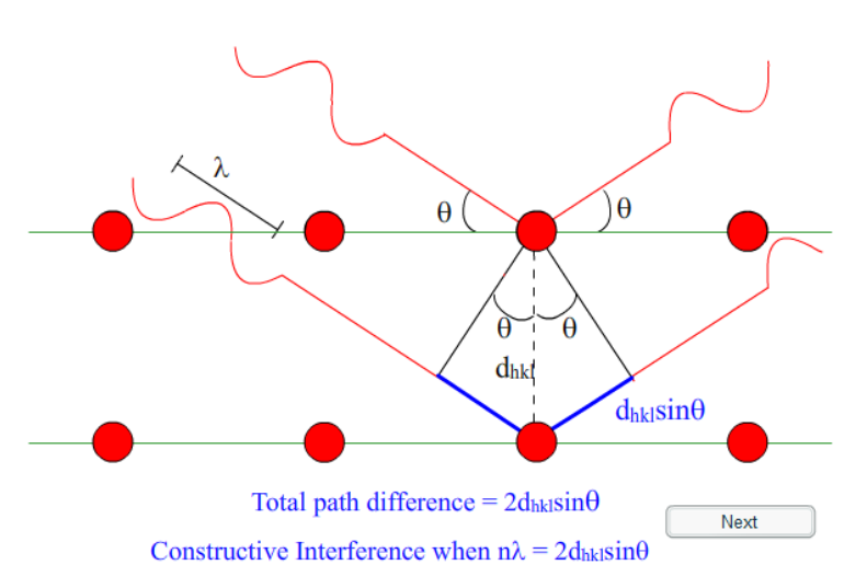
Braggs Law
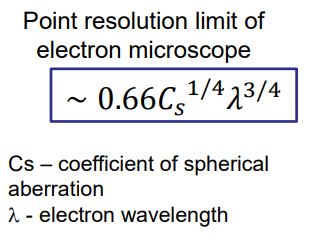
Point resolution limit
Aberration Corrected TEM
Spherical aberration in compensated by combining the converging lens with a suitable diverging lens - enabling a smaller electron beam