Section 3 - Non-Linear and Sensors
1/71
There's no tags or description
Looks like no tags are added yet.
Name | Mastery | Learn | Test | Matching | Spaced |
|---|
No study sessions yet.
72 Terms
Diode
has a forward bias, reverse bias, and reverse breakdown region; consist of a junction between 2 types of semiconduting material (n and p); potential barrier forms at PN junction; operated at a fixed current; V across depends on its temp.
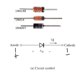
Forward Bias Region
if voltage (Vd) applied to diode +, large amounts of current flow for small V
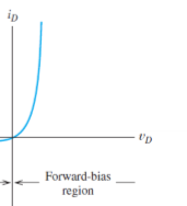
Reverse-bias Region
moderate - values of Vd, current (Id) is negligible

Reverse-breakdown Region
if large reverse-bias V applied to diode, large current magnitudes flow
n-type Material
large #’s of e- (or carriers) move freely
p-type material
+ charged particles (known as holes)
PN Junction
+ charged holes near junction jump from P → N; - charged e- near junction jump from N → P
Space Charge Region
formed in middle creating an electrical field from N → P
Potential Barrier
E field builds this; blocks e- from N → P and holes from P → N; doesn’t allow charges to keep changing
Coulomb’s Force
closer charges are to each other, the larger this

Forward Bias
this overcomes potential barrier; so once blocked, add V source in correct way
+ terminal repels holes to the junction and - terminal repels e- to the junction
space charge region narrows down
holes in P are able to migrate into N e- in N are able to drift into P (current now flows)
Reverse Bias
after blocked, flip + and - of v source
holes get attracted to - terminal and e- attracted to + terminal
results in increase of depletion band acting like an insulator that does not allow current flow
above a particular voltage, e- in N flow into P and holes in P into N, allowing a very high current
Small Signal Diodes
most common found in low/meidum-power electronic circuits;
linear change in V w/ temp. → useful as temp. sensors
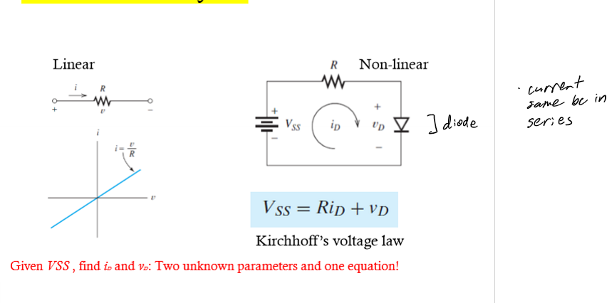
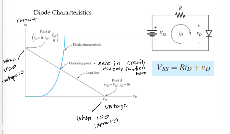
Load-line analysis
given VSS, find Id and Vd: 2 unknown parameters and 1 eq.; Vss = RId + vd
Zener Diode
operate in the breakdown region; uuseful in applications for which a constant V in breakdown is desirable
Voltage-Regulator
circuit provides a constant V to a load from a variable source; ex. box on a computer charger; change of the supply V changes the position, but not the slope of the load line
Rectifer Circuits
convert AC power into DC power; form basis for electronic power supplies and battery-charging circuits; delivers steady DC V
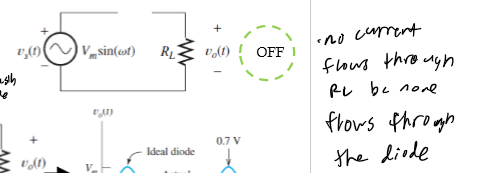
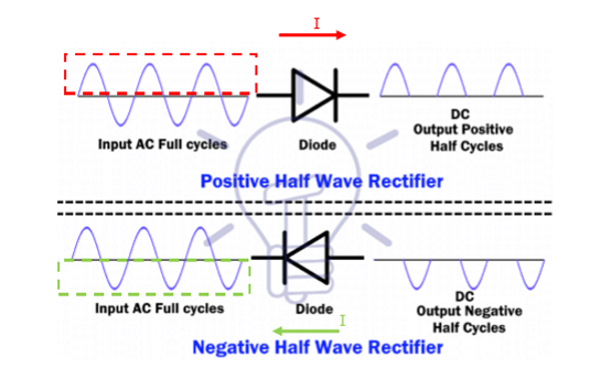
Half Wave Rectifer
when source V (Vs(t)) is +, diode is in forward-bias so if ideal diode assumed, source V appears across the load

Half Wave Rectifer part 2
when source V -, diode is reverse biased and no current flows through the load

Half Wave Rectifer pictures
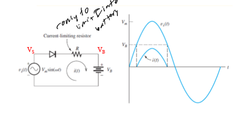
Battery-Charging Circuit
use a half-wave rectifer to charge a battery; current flows whenever the instanteous ac source V is higher than the battery VD
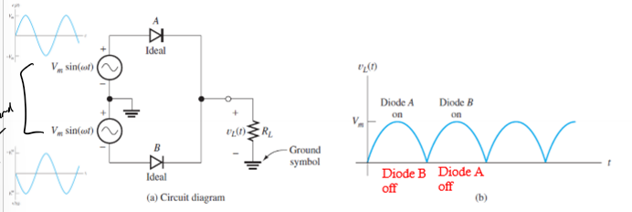
Full-wave Rectifer Circuits
2 halfwave rectifers w/ out of phase source V; combing half-wave circuits; when diode A is on, B is off and vide versa
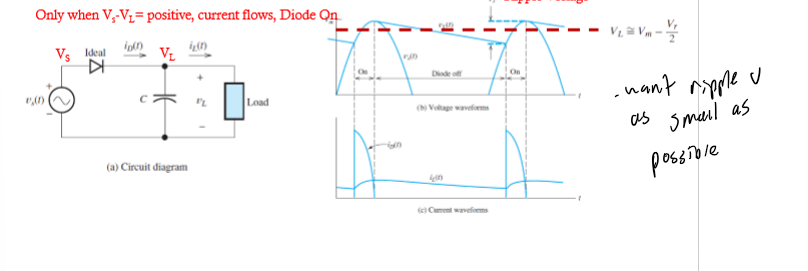
Smoothing Capacitor
smooths the rectifer output V; places across output terminals of the rectifer
Semiconductors - Diodes and Transistors
diodes - single p-n junction
transistors - amplifiers and logic gates (switching)
Transistor
amplifiers and logic gates (switching); FETs and BJTs
FETs
field-effect transistor; electric field controls the current flow
MOSFETs
metal-oxide-semiconductor FETs - smaller and easier to fabricate; very compact; electrically driven switch that allows and prevents curent flow w/o any mechanical moving part
What are MOSFETs made of?
a semiconducting material like silicon with doping
Doping
material allows only very little flow of electrons when it is in its pure form; when a proper impurity is introduced conductivity increases dramatically; N type and p type
N-type Doping
injecting impurity w/ extra free electons so adds free electrons → increases conductivity
P-type Doping
inject impurity w/ fewer electrons so adds hols allowing neighboring electrons flow into → conductivity increases
BJTs
bipolar junction transistor; passes large currents; layers of silicon doped with impurities to create n- and p-type regions
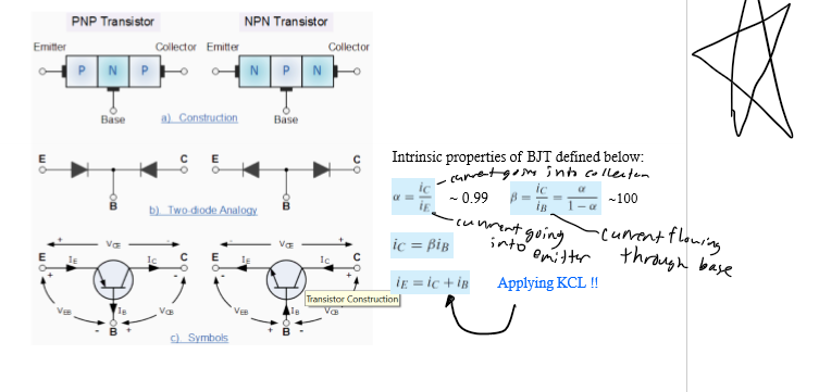
How are BJT’s like diodes?
pn junction forward biased by applying + voltage to p (base emitter); reverse biased by applying + v to n (base-collector)
How are BJT’s normally setup?
base-collector junction - reverse biased
base-emitter junction - forward biased
Diode - Forward bias overcomes potential barrior
inject impurity to silicon substrates → charges near
Common Emitter
type of transistor circuit; inverting amplifier circuit; gain = Vout/Vin = -R2/R1
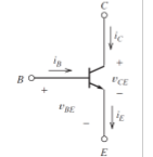
Transistor Regions
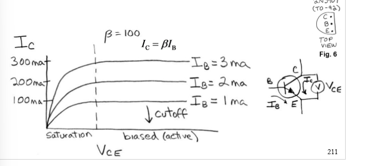
biased/active, cutoff, and saturation
Biased Region
Ic = Beta * Ib independent of Vce
Beta
constant for a given transistor; for our lab between 50-250
Cutoff
transistor turned off when Ib too small
Saturation
transistor “wide-open” w/ current limited elsewhere in the circuit
Amplifiers
used to increase the amplitudes of electrical signals (especially in sensors); has identical wavehsape to input, but with a larger output; can be inverting or non-inverting; can be in a cascade
Inverting Amplifier
output voltage is an inverted version of the input bc Av is a - number; changes sign
Non-inverting Amplifier
when Av is a + number; doesn’t change sign
Voltage-Amplifier
senses open-circuit V of the source and produces amplified V across the load independent of load impedance; infinite input impedance (no current) and 0 output impedance (output V is indepenent of load impedance)
Cascaded Amplifiers
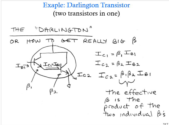
overall V gain is product of V gains of individual stages; overall current gain is product of current gains of individual stages; overall power gain is product of individual power gains; Av = Vo1/Vi1 Vo2/Vo1 = Av1*Av2
Switches
toggle, multipoint, momentary, and thermal; either “normally open” or “normally closed”
Toggle vs Momentary
spring-loaded, auto-return to default
Toggle Switch
one side of the other

Multipoint
spring-ish; force = on, no force = off

Momemtary Switch
button?

Thermal Switch
off or on depending on temperature

Sensors
thermistors, photic - photoresistors, photodiodes, and phototransistors, accelerometers, and IMUS
Thermistors
temperature sensor; resistance changes with temp.; can have vol + (PTC) or - (NTC) temp. coefficents; voltage divder; delta R = k*delta T
Photic Sensors
photoresistors and photodiodes
Photoresistors
light-dependent resistors (LDRs); resistance changes by adding free electrons to conductive path (usually a semiconductor); slow response time; as light increases = resistance decreases

Photodiodes
faster and more sensitive than LDRs; either photoconductive (reverse bias) or photovoltaic (0 bias); behave like regular diodes but light-sensitive
Photoconductive Mode
when it is reverse-biased; light adds electrons so increasing conductivity and current flow
Photovoltaic Mode
0 bias; light creates current flow in diode; solar cells
Phototransistor
light generates the voltage

Accelerometers
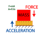
mass-spring system; micro-electro-mechanical-systems (MEMS) - fabricated in silicon; used in elevators
Inertial Measurement Units (IMUs)
integrated system to measure motion - translational or rotational; used in step counters, activity monitors, and gait-phase detectors
Actuators
light (LEDs), sound (speakers/buzzers), and force (motors); component of a machine that is responsible for moving and controlling a mechanism or system; ex. opening a valve
Sensor vs. Actuators
sensor is a device that changes a physical parameter → electrical output
actuator is a device that converts an electrical signal → physical output
sensor situated at input while actuator at outport port
sensor generates electrical signals while actuator results in production of energy (heat/motion)
Light-Emitting Diode (LED)
behave like regular diodes (PN junction, pass I when forward biased and block it when reverse biased); monochromatic - emits only at a single frequency; forward vias V is higher and varies w/ color; foward V drop = 1.8-3.3 V and operating current 2-20 mA
Why is forward bias V higher and vary w/ color?
bc photon energy (E=hv) where v is frequency and h is Planck’s constant
Solenoid
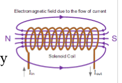
type of actuator; usually linear; driven by electromagnet; either on or off; fast operation, low maintainance with a long life and found in many common applications; generates an electric field
Relays
switch thrown by electromagnet pulling iron in switch lever against a spring; introduce gain - passes high I; can be either bistable or unstable
Bistable Relay Circuit
w/ memory; aka the latch; has + feedback → reinforces present state
Unstable Relay Circuit
aka the Buzzer; has - feedback → disavows present state and oscillates
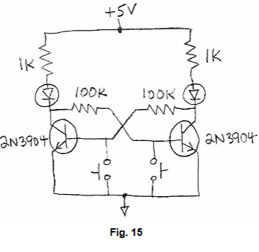
Flip Flop
bistable transistor circuit w/ + feedback; did in lab
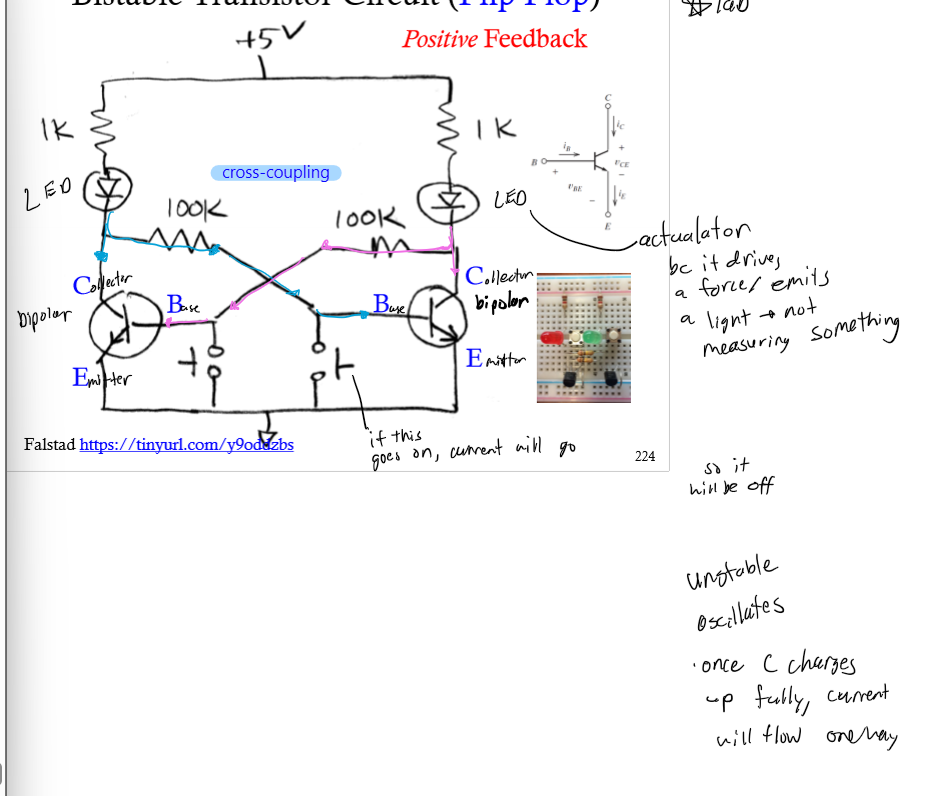
Flip Flop - Lab
if one of the transistors is conducting (in “saturation” mode), then its LED is “on”,
and the other transistor is not conducting (in “cut-off” mode) and its LED is off. Whichever transistor is on brings the base of the other transistor down near ground turning off the other transistor. The other transistor being off maintains a higher voltage at the first transistor’s base, keeping it on. Pushing the button associated with the “on” side of the circuit flips the state back and forth
