MEMS - Lithography I, II
 Call Kai
 Learn
Learn Practice Test
 Spaced Repetition
 Match
Match Flashcards
 Knowt Play
1/4

There's no tags or description
Looks like no tags are added yet.
Name | Mastery | Learn | Test | Matching | Spaced | Call with Kai | Chat |
|---|
No analytics yet
Send a link to your students to track their progress
5 Terms
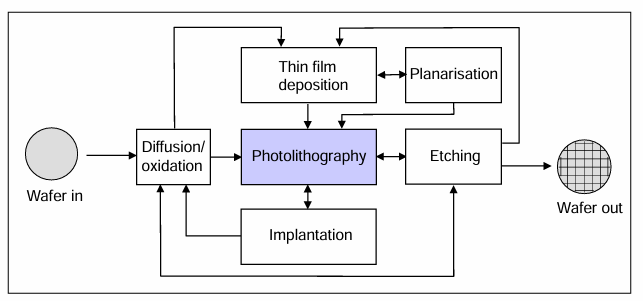
Photolithography in semiconductor fab
photolith used to define patterns at every stage
General steps
Vapour prime - adhedes resist to substrate
Spin-coat resist - pour on resist, spin for uniform layer
soft bake- drives off solvent/improves adhesion
expose- mask pattern transferred via UV light to latent image in resist
post-exposure bake- optional for most resists
develop- converts latent image to topographic pattern in resist
hard bake- improves chemical and physical robustness of patterned resist layer
inspect- for malformities
positive resist
exposure increases solubility, additive

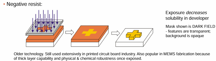
negative resist
exposure decreases solubility in developer
skipping sections on dip pen nanolith, non-imprint lith, scanning probe tehcniques, electron beam lithorgraphy, LIGA
asdf