Additional PhD defense questions
 Call Kai
 Learn
Learn Practice Test
 Spaced Repetition
 Match
Match Flashcards
 Knowt Play
1/25

There's no tags or description
Looks like no tags are added yet.
Name | Mastery | Learn | Test | Matching | Spaced | Call with Kai | Chat |
|---|
No analytics yet
Send a link to your students to track their progress
26 Terms
Background photovoltaic effect
Upon light absorption, excitons are initially created and consequently a current is generated which produces a potential when the charges are separated. This process is termed as the photovoltaic effect and forms the basic working principle of OPV and OPD devices..
The absorption of light in neat organic semiconductors generates localised excited states, previously called excitons. This electrically neutral state is able to diffuse in the material over a length of several tens of nanometers. As organic molecules are characterised by rather low dielectric constants, the exciton stays electrically bound as its surroundings do not screen the individual charges (in contrast to inorganic variants)Considering the strong binding force and relative short exciton lifetime, it is very unlikely that excitons are separated independently and a loss of energy, via a radiative or non-radiative pathway, is therefore most logic. To separate the excitons and generate free charges, a driving force should be available, after which the charges can be transported out of the material to be collected.
To realize efficient photoinduced charge separation in organic semiconductors, electron donor and acceptor materials are combined, as shown in Figure 1.7. The difference in the LUMO (or HOMO) levels is considered to be the driving force for the exciton separation. Before this event can take place, the excitons should reach the donor-acceptor interface. Hence, the process is limited by the diffusion length and lifetime of the exciton. As excitons are neutral species, their motion is
unaffected by an electrical field and it is the active layer morphology that is key for excitons to be able to reach a donor-acceptor interface. Excitons should be formed within their diffusion length from the interface, implying that a high degree of intermixing between the donor and acceptor materials should be accomplished. This prerequisite cannot easily be realized in bilayers, unless the layers are extremely thin, on the order of the exciton diffusion length. On the other hand, intimately mixed donor-acceptor blends drastically increase the amount of interface and consequently the number of excitons reaching it. The diffusion of excitons is mostly explained by long-range (intermolecular) electrostatic interactions but remains a topic of investigation. Once situated at the interface, the exciton loses some of its energy to become a charge-transfer (CT) state before finally separating into free charge carriers.[31] This two-step process is believed to be initiated by the difference in LUMO (or HOMO) energy of the donor and acceptor. The exciton in one material is changed to a CT state with the electron residing on the acceptor and the hole on the donor
Eventually, free charge carriers (polarons) are generated, increasing the conductivity of the material
Background OPD
OPD
A photodetector enables the detection of light using the photovoltaic effect. It can therefore be seen as a photodiode which generates a current when illuminated and no current when operating in dark conditions. As pristine organic materials have a very low charge generation yield due to the limited exciton dissociation tendency, the active layer should be composed of the aforementioned combination of electron donor and acceptor materials (not to be confused with the donor-acceptor or push-pull concept for decreasing the bandgap). Besides generating free holes and electrons, charges should be extracted from the active layer to produce an interpretable signal. The active layer is therefore sandwiched between two electrical contacts with specific energy levels that drive the charge extraction. This implies the use of a low work function cathode that collects electrons and a high work function anode that collects holes. Transparency of at least one of the electrodes is needed to allow light to reach the active layer. The two simplest possible device architectures with such requirements are shown in Figure 1.9, the first one with a bilayer and the second with a bulk heterojunction (BHJ) structure. As mentioned before, the diffusion length of excitons is rather short and a prerequisite for the bilayer architecture is therefore a limited active layer thickness to allow a sufficient amount of excitons to diffuse to the donor-acceptor interface. However, a thin layer is not able to absorb all the light hitting the device, resulting in a low production of excitons. Besides, the amount of interface available to separate excitons is also limited in this case. The BHJ is therefore a better alternative. The only downside of this type of structure is the possibility of dead ends for charge transport. Donor (acceptor) materials, capable of transporting positive (negative) charges, should be in contact with the anode (cathode) to have a proper charge collection. If this is not the case, the generated charges are likely to recombine before being collected at the metal electrodes
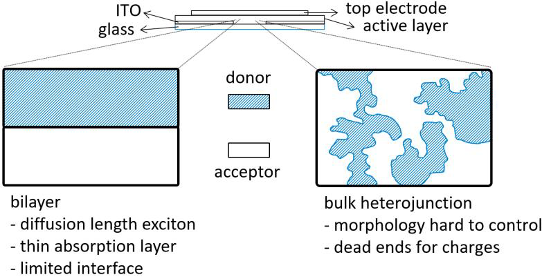
The key feature of photodetectors is the formation of a current upon illumination. As it is not the purpose to generate a power to an external load (as for OPVs), an external bias can be applied to facilitate the dissociation of the coulombically bound excitons and to aid charge carriers to reach the electrodes. The efficiency of charge generation and collection is only one of several device metrics to qualify the performance of photodetectors. Also the sensitivity (expressed in signal to noise ratio, noise equivalent power and detectivity), dark current (unavoidable noise sources), spectral response and more specific metrics like the dynamic range and response time are used to validate photodetectors. These figures of merit will be discussed in more detail in the following section.
difference OPD and OPV
The key feature of photodetectors is the formation of a current upon illumination. As it is not the purpose to generate a power to an external load (as for OPVs), an external bias can be applied to facilitate the dissociation of the coulombically bound excitons and to aid charge carriers to reach the electrodes.
Figures of merit for an OPD
Photocurrent
current generated when the OPD is illuminated
External quantum efficiency
extracted electrons/ incident photons
a high EQEPV means a large fraction of incoming NIR photons becomes electrical current available to drive an OLED
Responsivity R
photocurrent / incidient optical power
𝑅= 𝐽ph / 𝑃in = 𝑞𝜆/ℎ𝑐 x EQE [A/W]
units: A/W
directly related to the EQE but responsivity also depens on the wavelength because different wavelenghts ahve different energies
Dark current
= current flowwing wen no light is present
In conventional organic semiconductors, thermal generation of charge carriers is usually limited because of the relatively large bandgap, but for NIR-active materials the smaller bandgap makes thermally generated carriers more likely, which can increase the dark current. Defects such as pinholes or rough electrodes can also create unwanted pathways for charge injection.
Dark current itself is an average current; it is not exactly the same as noise.
noise current
Even if your average dark current is constant, the measured current fluctuates randomly.
These fluctuations are the noise current.
these fluctuations that determine whether a weak photocurrent can be distinguished from the background
low dark current is good, but low noise is what really determines sensitivit
Signal to noise ratio
S/N = useful signal/noise
S/N = 1 (signals is barely distinguishable from the noise)
Noise equivalent power (NEP)
= incident light power that produces a signal equal to the noise: S/N = 1
NEP is the minimum optical power that the detector can distinguish from its noise
lower NEP = better detector
Specific Detectivity D*
combines: responsivity, noise, device area, bandwidth
overall measure of how well a photodetector can detect weak light relative to its noise, normalized for detector area and bandwidth. A higher D∗ means a more sensitive detector.”
D* = A1/2 / NEP
D∗∝noise x A x f / R
Typical good OPDs can reach:
D∗∼10^12 Jones
Response time
how quickly the OPD reacts when the light is switched on or off
measure the time it takes to go from 10% to 90% of the max photocurrent when the light is turned on
or 90% to 10% when the light is turned off
for imaging: faster response = higher possible frame rate
speed is mainly determined by how quickly photogenerated charges are created, transported and extracted.
Linear dynamic range
range between the weakest and strongest illumination where the photocurrent generated is proportional to the incident light intensitiy
Jph∝Plight
larger range, detector works over a wider range of intensities
Spectral response
cut-off wavelength is the longest wavelength the OPD can still effectively detect.
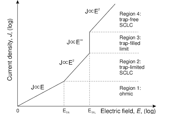
space-time limited current method
measures charge-carrier transport, mainly electron and hole mobility with a hole-only or electron-only device
you apply a voltage and measure the current density
for a single carrier device:
Region 1: at low voltage:
low amount of injected charge carriers: current is carried by small number of carriers already present
J is proportional to V - increase the voltage twice = twice as much current flows
Region 2 at higher voltage
organic semiconductors often contain trap states
injected carrriers get trapped in such states and don’t contribute to conduction
by increasing V, more and more traps get occupied until eventually they are all filled
now injected carriers can contribute to the conductivity rather than being trapped
the current therefore increases steeply and the slope changes: J∝Vm,m>2
the higher the voltage at which this occurs, the more traps need to be filled
region 3 - space-charge-limited current
now injecting a large number of mobil carriers
Because the material has finite mobility, these carriers don't instantly cross the device. Some accumulate inside the film.
That accumulation of electrical charge is called:
space charge
this accumulated charge create its own electric field, opposing further injection
so eventually the current not determined by: how easily can the electrode inject another hole
but How quickly can holes that are already inside the matirial move through it and get out of the way
in this regime: J∝μV2
so by fitting the curve the mobility of the charge carriers can be extracted
Current-voltage sweep measurement
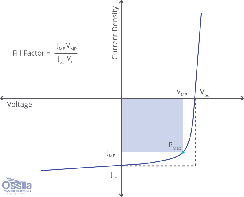
A current–voltage sweep measurement is a simple electrical measurement in which the voltage applied across a device is gradually changed while the corresponding current is recorded in the dark and under illumination
difference SCLC is that SCLC is used for single-carrier devices while J-V sweep on the complete photodiode
The illuminated curve shows:
JSC
the short-circuit current density, measured at V=0, which tells you how much photocurrent the OPD can generate without an external voltage;
VOC
the open-circuit voltage, where J=0, which tells you the maximum photovoltage the OPD can generate.
The dark curve shows
information about the dark current
Overview measurements
1. Molecule / thin film
UV–Vis–NIR absorption spectroscopy
Method: shine different wavelengths through the sample
Directly measured: transmitted light intensity vs wavelength
Calculated/derived: absorbance / absorption spectrum
Can determine:
λmax
absorption onset
extinction coefficient ε in solution
absorption coefficient α in thin film
Why: tells where and how strongly the molecule absorbs
Steady-state fluorescence / PL spectroscopy
Method: excite sample continuously with light and record emitted light
Directly measured: emitted light intensity vs wavelength
Obtained: fluorescence/PL spectrum
Can determine:
emission maximum
spectral shape
Stokes shift
fluorescence quenching
changes from solution → film → blend
Why: tells what happens to the optically excited state
Time-resolved fluorescence
Method: excite with a short laser pulse and follow emission over time
Directly measured: fluorescence intensity vs time
Calculated: fluorescence lifetime τ
Why: tells how quickly the excited state decays
Shorter lifetime can indicate additional decay pathways
PLQY / PLQE measurement
Method: measure absorbed and emitted photon numbers, often using an integrating sphere
Directly measured: absorbed light + emitted light
Calculated:
ΦPL=absorbed photons/emitted photons
Why: tells what fraction of excited states decay radiatively
Together with lifetime:
kr=τΦPL knr=τ1−ΦPL
Derived information: radiative vs non-radiative decay rates
So:
Time-resolved PL measures lifetime; PLQY measures emission efficiency; together they give decay rates.
Photostability measurement
Method: illuminate sample for a defined time, e.g. UV exposure in air
Directly measured: absorption/PL before and after or during illumination
Derived: percentage degradation / stability over time
Why: determines whether material survives illumination sufficiently for device use
Cyclic voltammetry — CV
Method: sweep electrode potential and measure electrochemical current
Directly measured: current vs applied potential
Obtained: oxidation and reduction potentials
Estimated from these: HOMO/LUMO energy levels
Why: check trends in energy levels and alignment with C60
Important:
CV does not directly measure the HOMO and LUMO. They are estimated from oxidation/reduction potentials.
UPS — ultraviolet photoelectron spectroscopy
Method: illuminate material with UV photons and measure emitted electrons
Directly measured: kinetic-energy distribution of photoelectrons
Derived: binding energies, ionization energy, work function, HOMO onset
Why: more direct experimental determination of occupied energy levels
DFT / TD-DFT
These are calculations, not experimental measurements.
DFT calculates: optimized geometry, electron density, orbitals/electronic structure
TD-DFT calculates: excitation energies, predicted absorption wavelengths, oscillator strengths
Why: predict and explain experimental trends
2. Charge-transport characterization
J–V sweep on a single-carrier device = SCLC measurement
Method: sweep voltage and measure current
Directly measured: J vs V
Device designed as:
hole-only, or
electron-only
SCLC analysis
Not really a separate measurement: it is a model used to fit the J–V data
Fit the space-charge-limited region using:
J∝μV2
Derived:
hole mobility μh, or
electron mobility μe
sometimes trap density
3. OPD characterization
J–V measurement
Method: sweep applied voltage
Directly measured: current density J vs voltage V
Usually done:
in dark
under illumination
Derived/read from curve:
JSC
VOC
dark current at a chosen bias
photocurrent
rectification behavior
So:
Measured: J(V)
Extracted: JSC, VOC, dark current, etc.
EQE(PV) measurement
Method: illuminate OPD wavelength-by-wavelength with a known photon flux
Directly measured: photocurrent at each wavelength + incident optical power/photon flux
Calculated:
EQEPV=incident photonsextracted electrons
Result: EQE spectrum vs wavelength
Why: tells how efficiently each wavelength is converted into electrical charge
Responsivity
Usually calculated from photocurrent and optical power, not a completely separate fundamental measurement.
R=Iphoto/Pincident
Units: A/W
Tells: electrical signal generated per watt of incoming light
Noise measurement
Method: measure current fluctuations, usually in the dark
Directly measured: noise current / noise spectral density
Combined with responsivity to calculate: NEP and detectivity
Detectivity D∗
Not directly measured
Calculated from: responsivity + noise + detector area/bandwidth
Tells: ability of OPD to detect very weak light
Higher D∗ = better
4. OLED characterization IVL measurement
I–V–L = current–voltage–luminance
Method: sweep voltage while monitoring electrical current and emitted brightness
Directly measured:
voltage V
current I or current density J
luminance L
Derived/read from curves:
turn-on voltage
current density vs voltage
luminance vs voltage
OLED operating behavior
So:
IVL is the measurement; turn-on voltage is one result extracted from it.
EL spectroscopy
Method: electrically drive OLED and measure emitted spectrum
Directly measured: emitted intensity vs wavelength
Result: EL spectrum
Determines:
emission maximum
spectral width
which material is emitting
unwanted emission from other layers
what are electrical frequencies and the electrical bandwidth?
Suppose you illuminate an OPD with constant NIR light. Ideally, it produces a constant photocurrent:
I(t)=constant
But if you switch the light on and off 10 times per second, the photocurrent also rises and falls 10 times per second:
f=10 Hz
If you modulate the light 1000 times per second:
f=1 kHz
So the electrical frequency describes how quickly the detector signal varies with time.
The same applies to noise. The dark current is not perfectly constant:
Idark(t)=Iaverage+small random fluctuations
Some fluctuations occur slowly:
0.1−10 Hz
while others occur much faster:
kHz, MHz, ...
We can mathematically separate these fluctuations according to their frequency. This gives a noise spectrum.
What does bandwidth mean then?
The measurement electronics do not necessarily record every possible frequency. You choose a range of electrical frequencies that you want to measure.
For example:
Δf=1000 Hz
could mean that your electronics accept signal variations up to roughly 1 kHz.
A signal changing at:
100 Hz
would be measured.
A signal changing at:
10 kHz
might be filtered out.
So you can think of the measurement system as a filter:
all electrical fluctuations→measurement bandwidth→measured signal Why does this matter for noise?
Because every frequency interval contains some noise.
If you measure only a narrow frequency range, you collect relatively little noise.
If you measure a much wider range:
1 Hz→1 MHz
you collect noise from many more frequency components.
For approximately white noise:
inoise∝Δf
So:
larger bandwidth→more measured noise
This is why bandwidth has to be specified when comparing photodetector sensitivity.
How do you evaluate whether your new BODIPY makes a good OPD?
First, under illumination we look at the photocurrent, EQE and responsivity to determine how efficiently NIR photons are converted into extracted charges. Then, in the dark, we measure dark current and especially noise. Combining the optical response with the noise gives us the NEP and specific detectivity, which tell us how weak a NIR signal the detector can actually detect. Finally, depending on the application, we also look at the spectral range, response speed and linear dynamic range
“Is the synthesis of these BODIPYs scalable?”
The project focusses more on making the BODIPYs and then analysing if they have the desired properties and performance. If we find one, optimization could be done afterwards.
A good analogy is pharmaceutical development: early synthetic routes are often multistep and relatively low-yielding because their first purpose is to access the molecule. Once a promising compound is identified, process chemists redesign and optimize the synthesis specifically for scale, improving yields, reducing purification steps and replacing procedures such as chromatography with more scalable methods like crystallization.”
“Is vacuum sublimation really scalable if you lose so much material?”
Material utilization is indeed a disadvantage of vacuum thermal evaporation. In our laboratory system, a large fraction of the sublimed material ends up on the masks and chamber walls rather than on the devices.
However, this does not mean that the technique is inherently unscalable. Vacuum thermal evaporation is already the dominant industrial manufacturing method for high-performance small-molecule OLED displays, where similarly expensive organic materials are deposited in complex multilayer stacks.”
this is in my FWO proposal: Scalability is not the largest concern at this stage as 100 mg (after sublimation) allows proper evaluation of material suitability. so how much do we need before sublimation? Does this refer to the sublimation during vacuum deposition or as a purification technique?
Purification by sublimation is a laboratory and industrial technique where a solid turns directly into a gas without melting into a liquid, leaving non-volatile impurities behind
Here, “100 mg (after sublimation)” almost certainly refers to sublimation as a purification step before device fabrication, not to the vacuum deposition itself.
The wording “100 mg after sublimation” means that you want approximately 100 mg of purified, device-grade material left after that purification step.
So assuming a recovery of 70-80% you would need 125 - 145 mg
Why should you do this project and not someone else?
I believe this project needs to happen because this self-driven upconversion has been proven to work. The absorption and device perfomance only limit it from becomming applicable in real world technologies. I am certain that with my PhD I will be able to solving these bottlenecks and bring UC closer to a technology ready for applications in NIR sensing and imaging.
I also think I am a very strong candidate given my background which fits exactly with the central challenge of the project. At the same time I’m very motivated and my strong commitment which is reflected by my grades.
Why BODIPY’s
It already has a large red-shift for being a rather small molecule, so extending the conjugated system can occur to a certain extent without exceeding the point where vacuum deposition is not possible anymore
It is alos metal free
For naphtalocyanohydrines the molecule is already large so extensions there would be limited for them to still be able to be vacuum deposited
it is photostable
shown to work in the UC device
highly tunable
experience in the DSOS group
What are spectrally and time-resolved fluorescence measurements and photoluminescence quantum efficiency measurements? And what are they used for? Do measure device or molecular properties?
These measurements are mainly photophysical measurements of the material, rather than measurements of the complete OPD device. They are used to understand what happens to the energy after a BODIPY molecule absorbs a photon.
Spectrally resolved fluorescence measures the emitted light as a function of wavelength, so it tells us where the molecule emits and can reveal changes in excited-state character, aggregation, excimer formation or charge-transfer states.
Time-resolved fluorescence measures how quickly the fluorescence decays after a short excitation pulse and gives the fluorescence lifetime, τ, which tells us how long the excited state survives. If the lifetime becomes shorter after a structural modification, this can indicate that an additional decay pathway has been introduced.
Photoluminescence quantum efficiency, PLQE, tells us what fraction of absorbed photons are re-emitted as fluorescence, so a high PLQE means radiative decay is efficient, while a low PLQE means that a large fraction of the excitation is lost through non-radiative or other competing pathways.
By combining the fluorescence lifetime and PLQE, we can estimate the radiative and non-radiative decay rates:
This is particularly important for NIR BODIPYs because pushing the absorption to longer wavelengths usually means reducing the energy gap, which can make non-radiative decay more efficient. We therefore want to know whether a new structural modification gives us redder absorption without introducing excessive energy losses. These measurements can be performed on the BODIPY in solution, as a neat thin film, or in a BODIPY:C60 blend. Comparing the neat material with the blend is especially useful: if the BODIPY fluorescence is strongly quenched after adding C60, this may indicate that electron transfer to C60 is competing efficiently with fluorescence, although additional measurements are needed to confirm that the quenching is productive charge transfer rather than another non-radiative process.
Why do the QC calculations?
allows us to select the most promising candidates based on the predicted properties
AND allows us to predict the photophysics and the results we will obtain in WP3, like the triplet states and the singlet states
what is furfural and how is it extracted from hemicellulose?


It is not really “extracted” directly from lignocellulose; it is produced from the hemicellulose fraction of lignocellulosic biomass such as wood, corn cobs, bagasse, or agricultural residues.
Lignocellulose consists mainly of:
cellulose + hemicellulose + lignin
Hemicellulose contains a large amount of pentose sugars, especially xylose. Under acidic conditions, the hemicellulose is first hydrolyzed to release these sugars:
xylan→xylose
The xylose is then dehydrated, losing three water molecules:
xylose−3H2Oacid, heatfurfural
Because furfural is relatively volatile, it can then be removed from the reaction mixture, commonly by steam distillation, and further purified by distillation.
the furopyrrol is then easily made through a Hemtsberger-knittel indolization:

What if the QC calculation fall through?
There is someone who will potentially do them, if not I will be trained to do them myself. I have some computational experience myself and we have a very good professor who is willing to train me if necessary danny vanpoucke.
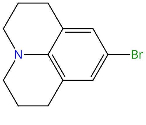
Yes, i can look in the database and if not, i will look for a precursor and synthesisiz it myself
boronic acid is pretty expensive: 360 dollars for 1g
but you can synthesize it starting from the bromide using BuLi in THF and adding trimethyl borate
the bromide is 16 dolars for 1g

Why did they choose Al as electrode and not Ag, as Ag is more reflective? Does it have to do with Al being able to reflect NIR light better?
Al was most likely chosen primarily because LiF/Al is a very well-established low-resistance electron-injecting cathode for this type of OLED architecture. The thick Al layer also provides sufficient optical reflection and participates in the optical cavity of the device. Ag would actually have somewhat better visible/NIR reflectivity, so the choice of Al is mainly electrical and technological rather than because Al reflects NIR better
“Actually, the paper uses both Al and Ag as top electrodes depending on the sample. Ag has somewhat better optical reflectivity, while Al is a well-established OLED electrode and also provides strong reflection. The choice therefore depends on the overall electrical and optical optimization of the stack rather than simply on NIR reflectivity.
-What kind of chemical calculations? What kind of software? What functional?
“We use DFT (density functional theory) to optimize the molecular geometry and investigate properties such as the frontier orbitals, and TD-DFT (time dependent density functional theory) to predict excited-state properties such as absorption wavelengths and oscillator strengths. These calculations are performed in collab with Prof. Champagne using Gaussian 16. Previous work with Prof. Champagne benchmarked 11 exchange-correlation functionals specifically for NIR BODIPYs and showed that M06-2X and M06-HF are the most reliable and gave the most consistent description of the relevant NIR-BODIPY singlet and triplet excitations and oscillator strengths., so we have a validated computational protocol rather than choosing a functional arbitrarily.”
Very simply, the calculation works like this:
You provide a molecular structure — the atoms and their approximate positions.
The software makes an initial guess for the electron density.
he program estimates where the electrons are distributed throughout the molecule:
ρ0(r)
From that density, it calculates an effective potential experienced by the electrons from the nuclei, repulsion of all other electrons and exchange and correlation effects for the last part exchange correlation functionals are needed
Using that potetntial, It solves the so-called Kohn–Sham equations to obtain molecular orbitals
these orbitals give a new estimate of the lowest energy position of the electrons based on their potential, which gives a new electron density
That new density is used again, and the cycle repeats until the density no longer changes significantly.
This is called a self-consistent field calculation:
ρ0→ρ1→ρ2→⋯→ρconverged
Once the electron density is converged, you can calculate properties such as:
molecular geometry, HOMO/LUMO, energies, charge distribution
Where does the “functional” come in?
The exact electron–electron interactions are still too difficult to calculate directly. DFT therefore uses an approximation called the exchange-correlation functional.
Notes immo
Annealing
do after spincoating, put it at high T for certain time (above Tg) to evaporate remaining solvent and allow changing of the morphology at nanoscale
not done after vacuum deposition, no solvent that needs removal, already provides good control over film thickness and morphology.
PEDOT:PSS
PEDOT:PSS could in principle serve as a hole-transport or hole-injection layer because of its high work function and good hole conductivity. However, it is generally solution-processed, while our upconverter is a complex vacuum-deposited multilayer stack. A vacuum-depositable p-doped transport material such as BF-DPB:F6-TCNNQ is therefore more compatible and allows better control of conductivity and layer thickness

substrate is first cleaned with various solvents

You can’t vacuum deposit ITO
need sputtering
looking into changing the reflective electrode with a transparent one, so light doesn’t have to travel back through the OPDs
always use 16 substrates, which is often to many
but useful for destructive charaterization
At what temperatures does vacuum deposition typically occur
For small organic molecules, the evaporation-source temperature is typically around 150–350 °C (max 400 °C). The exact temperature depends on the specific material and its vapor pressure. TGA can be used beforehand to assess its thermal stability and determine whether the material can be evaporated before it starts to decompose. The actual deposition temperature is then optimized experimentally to obtain a stable evaporation rate
what are the detectors used to control the rate of deposition and to know the layer thickness that has been deposited
“The deposition rate and nominal layer thickness are monitored using a quartz crystal microbalance (QCM). Material condensing on the quartz crystal changes its resonance frequency, and this is converted into a deposition rate and accumulated thickness. For co-evaporation, the rates of the individual materials are controlled separately to obtain the desired mixing ratio.”
there are 8 coils that contain materials including the acitve materials, HTL, ETL, electrodes,…
every 2 coils have their own sensor, so 4 sensors in total
so during co-evaporation the different materials need te be in coils with different detectors so their deposition rates can be controlled seperately.
why don’t you use different absorbers in the different OPD-layers?
In principle, we could use different absorbers in the different OPD layers, but that is not really the goal of this device. Unlike a tandem solar cell, where different absorbers are deliberately used to harvest different parts of the solar spectrum, our upconverter is mainly designed to detect a specific NIR wavelength range, even at very low light intensities. Using the same absorber in each OPD allows all subcells to respond to the same photons, while their photovoltages add in series. Using different absorbers would also make current matching much more difficult, because the current through the whole stack is limited by the lowest-performing OPD.
ups