Boylestad: MCQ in Bipolar Junction Transistors
1/55
There's no tags or description
Looks like no tags are added yet.
Name | Mastery | Learn | Test | Matching | Spaced | Call with Kai |
|---|
No study sessions yet.
56 Terms
B
In what decade was the first transistor created?
A) 1930s
B) 1940s
C) 1950s
D) 1960s
C
How many layers of material does a transistor have?
A) 1
B) 2
C) 3
D) 4
D
What is the ratio of the total width to that of the center layer for a transistor?
A) 1:15
B) 1:150
C) 15:1
D) 150:1
D
Which of the following is (are) the terminal(s) of a transistor?
A) Emitter
B) Base
C) Collector
D) All of the above
B
List the types of bipolar junction transistors.
A) ppn, npn
B) pnp, npn
C) npp, ppn
D) nnp, pnp
B
Transistors are _______-terminal devices.
A) 2
B) 3
C) 4
D) 5
A
How many carriers participate in the injection process of a unipolar device?
A) 1
B) 2
C) 0
D) 3
C
Which component of the collector current IC is called the leakage current?
A) Majority
B) Independent
C) Minority
D) None of the above
C
For a properly biased pnp transistor, let IC = 10 mA and IE = 10.2 mA. What is the level of IB?
A) 0.2 A
B) 200 mA
C) 200 µA
D) 20.2 mA
A
Calculate minority current ICO if IC = 20.002 mA and IC majority = 20 mA.
A) 2 µA
B) 0.002 µA
C) 2 nA
D) 2 pA
D
Which of the following regions is (are) part of the output characteristics of a transistor?
A) Active
B) Cutoff
C) Saturation
D) All of the above
C
In which region are both the collector-base and base-emitter junctions forward-biased?
A) Active
B) Cutoff
C) Saturation
D) All of the above
B
How much is the base-to-emitter voltage of a transistor in the "on" state?
A) 0 V
B) 0.7 V
C) 0.7 mV
D) Undefined
C
In the active region, while the collector-base junction is ______-biased, the base-emitter is ______-biased.
A) forward, forward
B) forward, reverse
C) reverse, forward
D) reverse, reverse
C
What is βdc equal to?
A) IB / IE
B) IC / IE
C) IC / IB
D) None of the above
D
For what kind of amplifications can the active region of the common-emitter configuration be used?
A) Voltage
B) Current
C) Power
D) All of the above
A
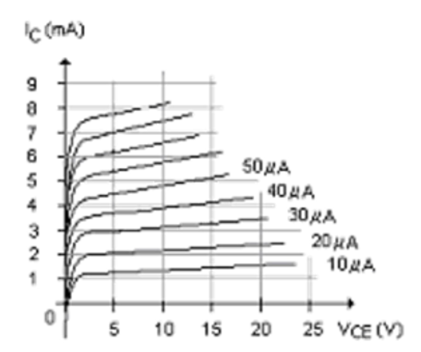
Use this table of collector characteristics to calculate βac at VCE = 15 V and IB = 30 µA.
A) 100
B) 106
C) 50
D) 400

D
Calculate βdc at VCE = 15 V and IB = 30 µA.
A) 100
B) 116
C) 50
D) 110

D
Which of the following configurations can a transistor set up?
A) Common-base
B) Common-emitter
C) Common-collector
D) All of the above
C
Determine the value of α when β = 100.
A) 1.01
B) 101
C) 0.99
D) Cannot be solved with the information provided
C
What is the most frequently encountered transistor configuration?
A) Common-base
B) Common-collector
C) Common-emitter
D) Emitter-collector
D
βdc for this set of collector characteristics is within _____ percent of βac.
A) 2
B) 5
C) 7
D) 10
D
What is (are) the component(s) of most specification sheets provided by the manufacturer?
A) Maximum ratings
B) Thermal characteristics
C) Electrical characteristics
D) All of the above
D
Most specification sheets are broken down into _______.
A) maximum ratings
B) thermal characteristics
C) electrical characteristics
D) All of the above
B
An example of a pnp silicon transistor is a 2N4123.
A) True
B) False
D
Which of the following equipment can check the condition of a transistor?
A) Current tracer
B) Digital display meter (DDM)
C) Ohmmeter (VOM)
D) All of the above
D
Which of the following can be obtained from the last scale factor of a curve tracer?
A) hFE
B) αdc
C) αac
D) βac
A
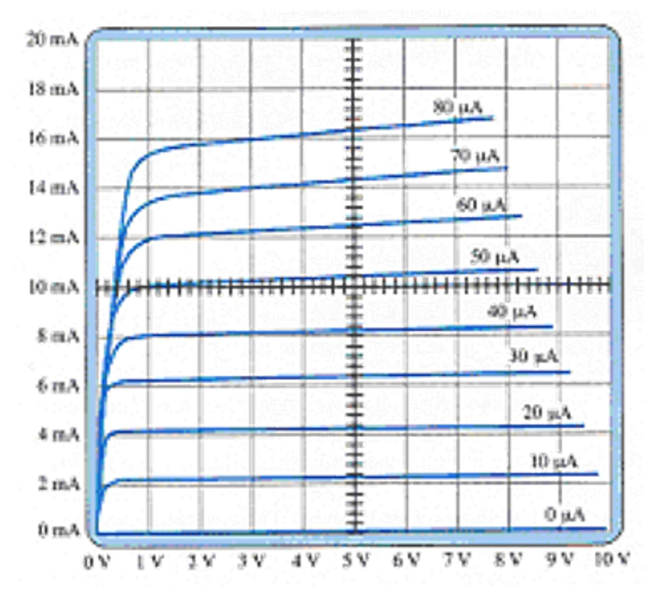
Calculate βac for IC = 15 mA and VCE = 5 V.
A) 200
B) 180
C) 220
D) None of the above
A
What range of resistor values would you get when checking a transistor for forward- and reverse-biased conditions by an ohmmeter?
A) 100 Ω to a few kΩ, exceeding 100 kΩ
B) Exceeding 100 kΩ, 100 Ω to a few kΩ
C) Exceeding 100 kΩ, exceeding 100 kΩ
D) 100 Ω to a few kΩ, 100 Ω to a few kΩ
A
What does a reading of a large or small resistance in forward- and reverse-biased conditions indicate when checking a transistor using an ohmmeter?
A) Faulty device
B) Good device
C) Bad ohmmeter
D) None of the above
A
How many individual pnp silicon transistors can be housed in a 14-pin plastic dual-in-line package?
A) 4
B) 7
C) 10
D) 14
B
All amplifiers should have at least _____ terminals with _____ terminal(s) controlling the flow between _____ other terminal(s).
A) 2, 1, 1
B) 3, 1, 2
C) 3, 2, 1
D) 3, 0, 3
C
The outer layers of a transistor are _______ the sandwiched layer.
A) much smaller than
B) the same as
C) much larger than
D) None of the above
A
The doping of the sandwiched layer is _______ that of the outer layers.
A) considerably less than
B) the same as
C) considerably more than
D) None of the above
D
The lower doping level _______ the conductivity and _______ the resistivity of the material.
A) increases, decreases
B) increases, increases
C) decreases, decreases
D) decreases, increases
B
The term bipolar reflects the fact that _______ and _______ participate in the injection process into the oppositely polarized material.
A) holes, neutrons
B) holes, electrons
C) neutrons, electrons
D) None of the above
C
One p-n junction of a transistor is _______-biased and the other one is _______-biased in the active region.
A) reverse, reverse
B) forward, forward
C) reverse, forward
D) None of the above
B
he magnitude of the base current is typically on the order of _______ as compared to _______ for the emitter.
A) µA, µA
B) µA, mA
C) mA, µA
D) mA, mA
B
The base current is the _______ of the emitter and collector currents.
A) sum
B) difference
C) product
D) None of the above
A
The _______ region is the region normally employed for linear (undistorted) amplifiers.
A) active
B) cutoff
C) saturation
D) All of the above
C
In the cutoff region the collector-base junction is _______-biased and the base-emitter junction is _______-biased for a transistor.
A) reverse, forward
B) forward, reverse
C) reverse, reverse
D) forward, forward
D
In the saturation region the collector-base junction is _______-biased and the base-emitter junction is _______-biased for a transistor.
A) reverse, forward
B) forward, reverse
C) reverse, reverse
D) forward, forward
B
For practical transistors the level of alpha typically extends from _____ to _____ with most approaching the higher end of the range.
A) 0.0, 1
B) 0.90, 0.998
C) 50, 400
D) None of the above
C
Typical values of voltage amplification for the common-base configurations vary from _______ and the current gain is always _______.
A) less than 1, 50 to 300
B) 50 to 300, larger than 1
C) 50 to 300, less than 1
D) larger than 1, 50 to 300
C
If a value of beta.gif is specified for a particular transistor configuration it will normally be used for _____ calculations.
A) ac
B) dc
C) ac and dc
D) None of the above
B
The common-collector configuration has a ______ input impedance and a ______ output impedance.
A) low, high
B) high, low
C) high, high
D) low, low
D
The active region of a transistor is bounded by the _______.
A) cutoff region
B) saturation region
C) power dissipation curve
D) All of the above
B
The "on" and "off" characteristics refer to _____ limits while the small-signal characteristics indicate the parameters of importance to _____ operation.
A) ac, dc
B) dc, ac
C) ac, dc and ac
D) dc and ac, dc
C
The step function (per step) of a curve tracer reveals the scale for _______.
A) collector current IC
B) VCE voltage
C) base current IB
D) All of the above
D
The level of _____ is determined and displayed by advanced digital meters.
A) VCE
B) IB
C) IC
D) βdc
A
The level of _____ is determined and displayed by advanced digital meters if using diode-testing mode.
A) VBE
B) IC
C) IB
D) IE
A
When checking a transistor by ohmmeter, a relatively _______ resistance is displayed for a forward-biased junction and ______ resistance for a reverse-biased junction.
A) low, very high
B) low, low
C) high, high
D) high, very low
B
An OL indication on an advanced digital meter indicates _______ while checking a transistor.
A) forward bias
B) reverse bias
C) definitely a defective transistor
D) None of the above
A
If the positive lead of an ohmmeter is connected to the base and the negative lead to the emitter, a low resistance reading would indicate a ______ transistor and a high resistance reading would indicate a ______ transistor.
A) npn, pnp
B) pnp, npn
C) npn, npn
D) pnp, pnp
B
The leads of a transistor are typically made of _______.
A) gold
B) aluminum
C) nickel
D) All of the above
D
There is(are) _______ in the internal construction of a TO-92 package.
A) gold bond wires
B) a copper frame
C) epoxy encapsulation
D) All of the above