Lecture 14 - Non-Gas Dosimeters and Semiconductors
1/99
Earn XP
Description and Tags
ONCOL 243 - Radiation Safety. University of Alberta
Name | Mastery | Learn | Test | Matching | Spaced |
|---|
No study sessions yet.
100 Terms
what are scintillators
materials that emit visible light or UV light after interacting with ionizing radiation.
When were scintillation detectors first observed, and by whom?
Scintillation was first observed by Roentgen in barium platinocyanide due to X-rays.
What are the two types of signal amplification used in scintillation detectors?
Film-screen amplification for storage.
Electronic devices such as photomultipliers (PMTs), photodiodes, and image intensifiers.
How mode do scintillation detectors operate in?
operate in pulse mode
what is the most common scintillator used in nuclear medicine?
Sodium iodide activated with thallium (NaI(Tl)) is used in most nuclear medicine applications, particularly for radiopharmaceuticals with energies ranging from 70-365 keV.
does sodium iodide activated with thallium (NaI(Tl)) have a high or low conversion efficacy?
high conversion efficacy, with 13% of deposited energy converted into light.
applications of NaI(Tl) scintillators
NaI(Tl) scintillators are coupled to photomultiplier tubes (PMTs) and used in thyroid probes and gamma well counters.
What type of scintillators are used as PET detectors?
Lutetium oxyorthosilicate (LSO) and bismuth germanate (BGO) scintillators are commonly used as PET detectors.
PET detectors require high detection efficiency for 511 keV photons and fast signal response
What type of scintillators are used in CT detectors?
Cadmium tungstate and gadolinium oxysulphide (GOS) scintillators are typically used in CT detectors.
scintillators are coupled to photodiodes to handle high X-ray flux in current mode.
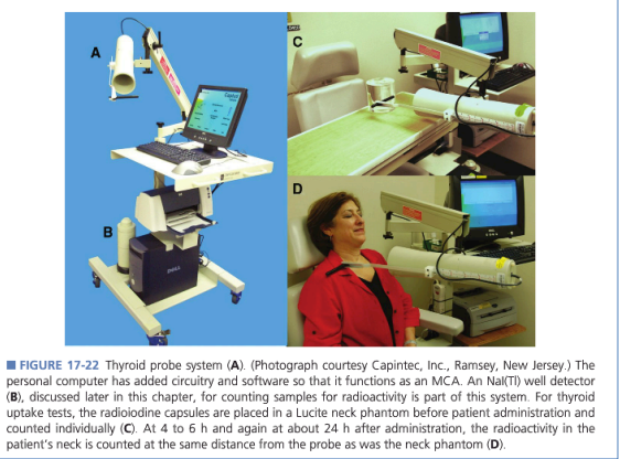
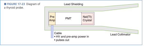
how do thyroid probe scintillator detectors work?
Thyroid probe scintillator detectors work by detecting gamma radiation emitted from the thyroid gland using NaI(Tl) scintillators, which convert gamma rays into visible light. This light is then converted into an electrical signal by photomultiplier tubes, allowing for the measurement of radioactivity.
no image is produced, just a count
What are the two main functions of a photomultiplier tube (PMT)?
1) Conversion of visible or UV photons into an electrical signal.
2) Signal amplification, ranging from millions to billions, from scintillators.
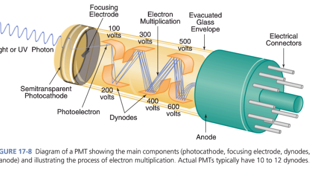
What are the main components of a photomultiplier tube (PMT)?
A PMT consists of an evacuated glass tube containing a photocathode, 10-12 dynodes, and an anode.
What is the role of the photocathode in a photomultiplier tube (PMT)?
The photocathode converts photons into electrons, typically converting 5 photons into one electron.
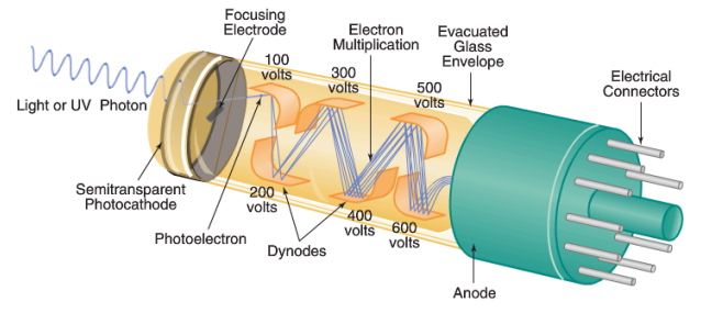
How does a photomultiplier tube (PMT) work?
A photomultiplier tube (PMT) works by converting visible or UV photons into electrons through a photocathode. These electrons are then amplified by a series of dynodes, where each dynode causes the emission of additional electrons. This results in a significant increase in the number of electrons, leading to a high-intensity electrical signal. The final amplified signal is collected at the anode, allowing for detection and measurement of the initial light signal.
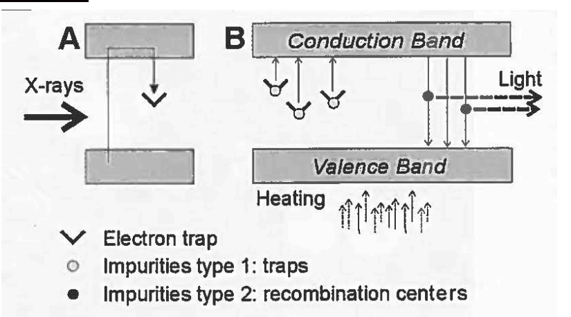
What is electron trapping
Electron trapping occurs when electrons are trapped in an excited state and do not immediately emit light. They can be released later to emit light through various methods.
How can trapped electrons be released to emit light?
Trapped electrons can be released by heating (as in thermoluminescent dosimeters or TLDs) or by exposure to laser light (stimulated luminescence, as in optically stimulated luminescence or OSLs).
What are thermoluminescent dosimeters (TLDs) made of?
TLDs are made of Lithium Fluoride (LiF), with a Zeff (atomic number) similar to that of tissue. The light emission is approximately proportional to the tissue dose.
What are optically stimulated luminescence (OSLs) made of?
OSLs are made of aluminum oxide (Al₂O₃) activated with carbon. The Zeff of aluminum oxide is much higher than that of soft tissue, so compensations are needed when calculating the dose.
What are the components of a film dosimeter?
A film dosimeter consists of a base (usually polyester) coated on one or both sides with a radiosensitive emulsion made of silver bromide embedded in gelatin.
How does radiation affect the film in film dosimetry?
When radiation hits the film, it causes silver to be produced which creates a latent image that is later processed
How is the latent image on the film processed?
During processing, other silver ions (Ag+) are reduced to silver (Ag), and the unreacted silver halide is washed out. Only the areas hit by radiation appear black.
What is film dosimetry good at determining?
Isocurves for dose distribution with wedges
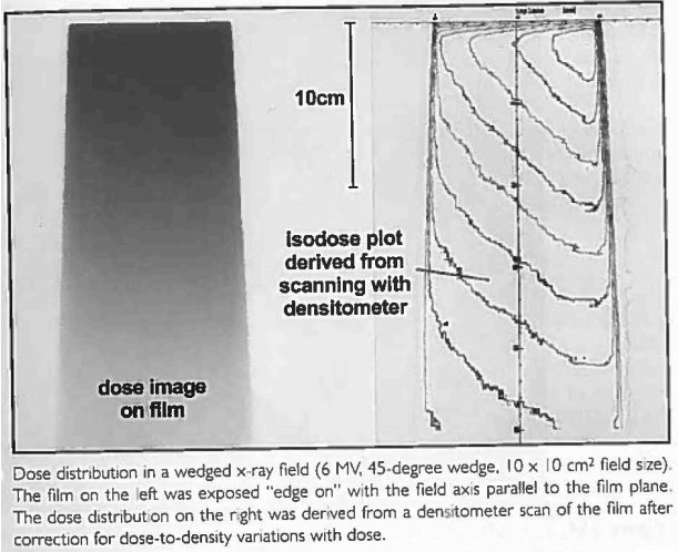
What is the spatial resolution of film dosimetry?
The spatial resolution of film dosimetry is better than 1 mm, theoretically down to 1 µm (one grain of the emulsion).
What are some key applications of film dosimetry?
Film dosimetry is useful for:
Dosimetry when wedges are used or during rotation therapy.
Determining the position of the patient relative to the beam.
Checking the X-ray field for quality assurance (QA).
Finding the center of the beam using a spoke pattern exposure.
What does computed radiography use instead of film?
Computed radiography uses a photo-stimulating storage phosphor in an imaging plate instead of film.
What is the role of the phosphor in computed radiography?
The phosphor (typically barium-based) stores the energy caused by radiation.
How is the stored energy in computed radiography read out?
The stored energy is read out by optical stimulation using a laser
what features would an Ideal Dosimeter have (non-realistic)
● instantaneous response
● distinguish different type of radiation
● accurately measure the equivalent dose
● wide radiation range: ~kV to MeV
● independent of angle of radiation
● small, light, easy to use, cheap, robust, environment
independent (humidity, temp, pressure)
What is the goal of dosimeters
to measure absorbed dose – energy absorbed per unit mass
do dosimeters use direct measurements
no, the quantity of radiation measured must be converted into absorbed dose
three types of individual dosimeters
film badges
storage media dosimeters (TLD, OSL)
Pocket dosimeters
Why is the dose to the film not equal to the dose in tissue in film badges?
The silver bromide in the film has a higher Zeff than tissue, so the dose to the film is not equal to the dose in tissue.
What features are included in a film badge to calculate the soft tissue dose?
Film badges include several filters (such as lead, copper, and aluminum) to calculate the soft tissue dose and the energy range of the radiation.
What is the purpose of the "open window" in a film badge?
The "open window" (an uncovered area) in a film badge is used to detect medium and high-energy beta radiation.
Pros and Cons of Film Badges
Pros
Small, light, inexpensive, easy to use
Cons
Moisture, temperature can damage the film.
What is a thermoluminescence dosimeter?
A device that applies heat (thermo) to a crystal, causing it to emit light (luminescence). The intensity of the light depends on the dose of ionizing radiation absorbed by the crystal before heating.
How does a thermoluminescence dosimeter (TLD) work?
The dosimeter contains a crystal that absorbs ionizing radiation. When heat is applied, the crystal releases stored energy as light (luminescence). The intensity of the light emitted is directly proportional to the amount of radiation the crystal absorbed before heating.
What is the most commonly used material in thermoluminescence dosimeters?
The most commonly used material is LiF:Mg,Ti (lithium fluoride doped with magnesium and titanium).
What are the characteristics of the crystals used in thermoluminescence dosimeters?
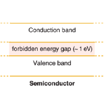
The crystals are nonconductive and phosphor-based. After radiation, some electrons get trapped between the conduction and valence bands due to imperfections in the crystal, with a gap of a few electron volts.
How does the intensity of radiation affect the thermoluminescence dosimeter?
The number of electrons trapped in the crystal depends on the intensity of the radiation. More radiation leads to more electrons being trapped.
What happens when the thermoluminescence dosimeter is heated?
When heated, the trapped electrons gain energy, move to the conduction band, and release energy in the form of light as they move "down" to a lower energy state.
move up from valence band to conduction band, and then drop back down

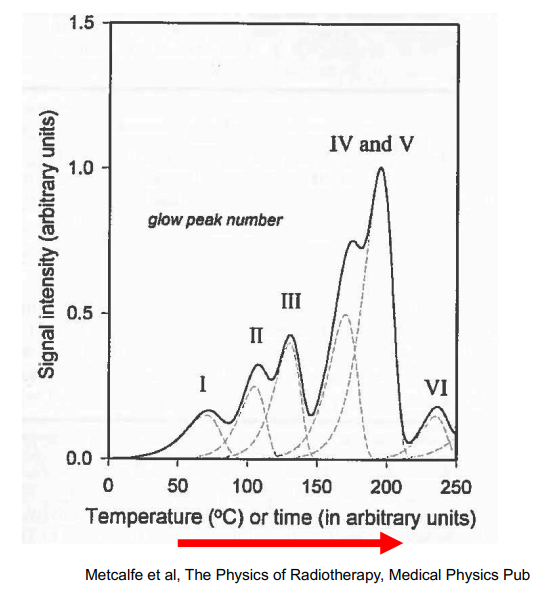
What are TLD glowcurves?
TLD glowcurves are graphs that represent the intensity of light emitted by a thermoluminescence dosimeter (TLD) as it is heated. The curve shows the relationship between temperature and the emitted light intensity, which provides information about the radiation dose absorbed by the dosimeter.
Pros of TLD
Wide dose response: 100 μSv to 10 Sv
Reusable
Can be used for up to ~6 months
Energy response:
0.766 to 5 MeV for beta radiation
20 keV to 6 MeV for X-ray and gamma
• (+) Zeff close to that of tissue thus dose close to tissue dose
Cons of TLD
More expensive than film badges
Complex readout process
Thermal history impacts glow peaks
Do not provide permanent record (heating removes deposited information)
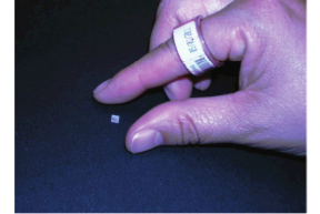
What are TLDs mostly used for
finger ring / extremity dosimeters
How does OSL (Optically Stimulated Luminescence) work?
OSL works on similar principles to TLD, but instead of heat, laser light is used to release trapped electrons. The luminescent light is then recorded at a 90° angle with filtration.
What material is commonly used in OSL dosimeters?
OSL dosimeters typically use crystalline aluminium (Al₂O₃:C).
What are the advantages of OSL over TLD?
OSL offers faster read-out and higher spatial resolution, as the "reading" light can be applied locally to specific areas of the dosimeter.
reusable
Can differentiate between static and dynamic exposure (due to image of the filters pattern)
What is a disadvantage of OSL dosimeters compared to TLD?
OSL dosimeters are more expensive than TLD dosimeters.
What is the memory cell used in a Direct Ion Storage Device?
The memory cell is a gas ion chamber.
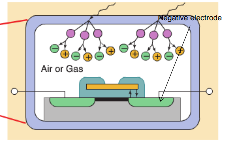
How does the Direct Ion Storage Device work?
X-ray or gamma radiation interacts with the chamber's wall, causing secondary electrons to ionize the gas. Positive ions move to the central negative electrode, reducing the voltage in proportion to the dose.
How is the data from a Direct Ion Storage Device transmitted and processed?
The data is sent to a computer via USB, where a computer algorithm analyzes the typical photon energy spectrum.
What type of radiation can the Direct Ion Storage Device not measure?
It cannot measure beta radiation.
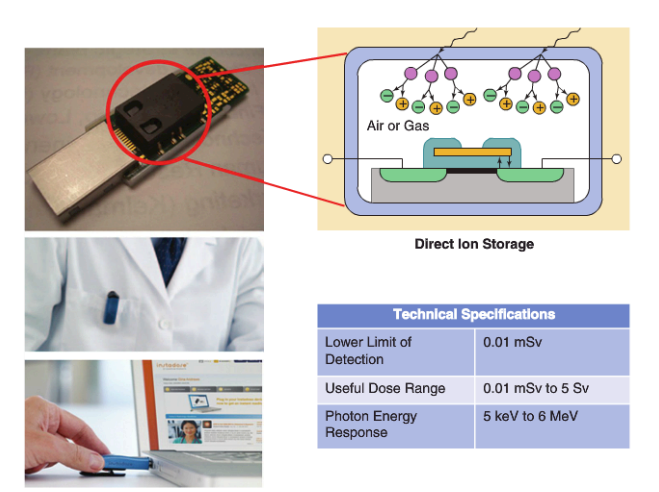
Pros and Cons of Direct Ion Storage Device
Pro: data from device can be intrepreted as soon as plugged into USB
good for power plant workers who may have had accidental contamination
Con: rather expensive
What is a "pocket dosimeter"?
A pocket dosimeter is a small, portable ion chamber that can be read immediately after exposure.
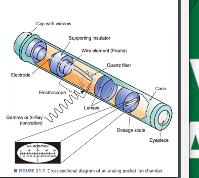
How does a pocket dosimeter work?
Radiation-induced ionization reduces the Coulomb force, causing the fiber to bend. This bending is visible through an optical lens, allowing for a quick reading.
When are pocket dosimeters commonly used?
Pocket dosimeters are commonly used when high doses are expected.
What is a limitation of pocket dosimeters?
Pocket dosimeters are small but may produce errors if dropped.
How do digital pocket dosimeters differ from traditional pocket dosimeters?
Digital pocket dosimeters use solid-state electronics and radiation-sensitive semiconductor diodes.
Where should dosimeters be placed on the body?
Dosimeters should be placed where the highest dose is expected or on the most sensitive areas, such as at waist or shirt-pocket level, or in front of the lead apron during fluoroscopy (sometimes a second dosimeter is placed underneath the apron).
What happens when the body is placed between the radiation source and dosimeter?
The dosimeter will record an average dose, potentially underestimating the dose received by the individual.
Where should a dosimeter be placed for pregnant women?
Pregnant women should wear an additional dosimeter at the waist.
What is the purpose of having a control dosimeter?
One dosimeter is kept aside from radiation sources as a control to ensure accurate readings and detect any possible environmental or background radiation.
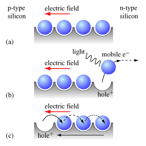
What is a semiconductor?
A semiconductor is a material that has electrical conductivity between that of a conductor and an insulator. It allows current to flow through it under certain conditions, typically through the movement of electrons and holes in its crystal lattice.
How is current carried through a semiconductor crystal lattice?
Current is carried by charge carriers: electrons (negative charge) and holes (positive charge, which are vacancies where electrons are missing).
What are holes in a semiconductor?
Holes are vacancies in the lattice where an electron is missing. They can move through the lattice as if they were positively charged particles.
What is the analogy between electrons and holes in a semiconductor?
Electrons and holes in a lattice are analogous to an ion pair, where the electron is negative and the hole is positive
What is the difference between valence electrons and conduction electrons in a semiconductor?
Valence electrons are in the lower energy "valence band" and do not move, as they are involved in bonding. Conduction electrons are in the higher energy "conduction band" and are free to move, allowing current to flow.
What is the role of electrons in the valence band of a semiconductor?
Electrons in the valence band are involved in bonding tasks within the crystal lattice and do not move freely.
What is the role of electrons in the conduction band of a semiconductor?
Electrons in the conduction band have higher energy and are free to move, allowing current to flow through the semiconductor.
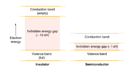
What characterizes a semiconductor in terms of energy bands?
A semiconductor has a narrow energy band gap, meaning the difference between the valence band and conduction band is smaller than in an insulator.
What are examples of semiconductor materials?
Silicon, germanium, gallium arsenide
What are the three ways electrons caan be promoted from the valence band to the conduction band of a semiconductor?
Ionizing Radiation
Visable/UV Light
Thermal Energy
What is a hole in semiconductor physics?
A hole in semiconductor physics is the absence of an electron in the valence band, which acts as a positive charge carrier. Holes are created when electrons are excited to the conduction band.
How does a hole "move" in a semiconductor?
A hole moves through a semiconductor by the movement of electrons filling the vacancy left behind, creating the illusion of a positive charge carrier moving in the opposite direction.
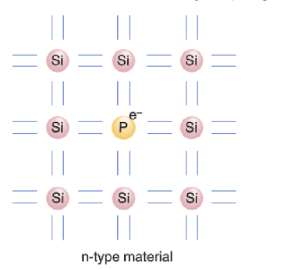
What is semiconductor doping?
The process of adding impurities to a semiconductor to create either n-type or p-type material.
What is an n-type semiconductor?
An n-type semiconductor is a type of semiconductor that has been doped with elements that provide extra electrons, resulting in a negative charge carrier concentration. This enhances its electrical conductivity.
What is a p-type semiconductor?
A p-type semiconductor is a type of semiconductor that has been doped with elements that create holes, resulting in a positive charge carrier concentration. This improves its electrical conductivity.
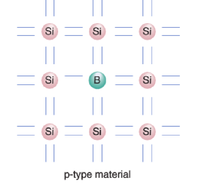
Why do p-type semiconductors have lower mobility?
P-type semiconductors have lower mobility because the holes created by doping are less mobile than electrons in n-type semiconductors, leading to reduced charge carrier movement.

What is a semiconductor diode?
A semiconductor diode is a device that allows current to flow in one direction only, created by joining p-type and n-type semiconductors, enabling its use in rectification and switching applications.
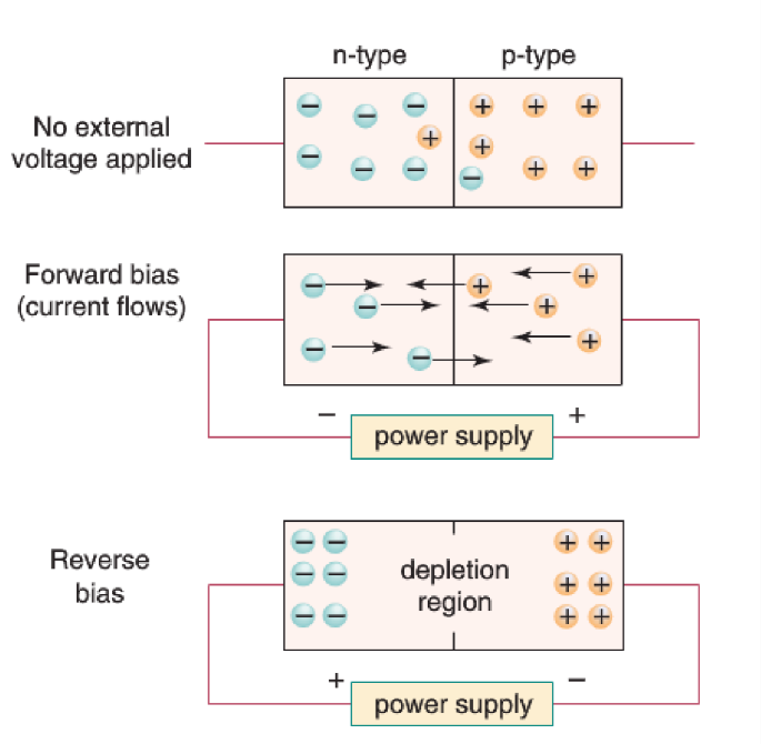
What happens in forward bias of a semiconductor diode?
In forward bias, the p-type side is connected to the positive terminal and the n-type side to the negative terminal of a power source, reducing the potential barrier and allowing current to flow through the diode.

What happens in reverse bias of a semiconductor diode?
In reverse bias, the p-type side is connected to the negative terminal and the n-type side to the positive terminal of a power source, increasing the potential barrier and preventing current from flowing through the diode.
creates an insulating depletion zone, allowing very little current to flow.
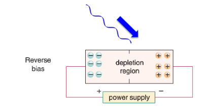
What can depletion regions be used for?
radiation measurement and detection
How do semiconductor radiation detectors work?
They operate by creating electron-hole pairs in the depletion region when radiation interacts with the semiconductor material, allowing for current measurement.
They generate a charge proportional to the deposited energy, allowing them to function as spectrometers.
Why is cooling sometimes used in semiconductor radiation detectors?
To prevent thermal energy from exciting electrons and causing unwanted noise.
How does the quantum detection efficiency of semiconductors compare to scintillators?
Semiconductors have lower quantum detection efficiency than scintillators.
three types of semiconductor radiation detectors?
Photodiodes
detect light
Silicon Diode
MOSFET Transistor
What is a photodiode?
A semiconductor diode that converts light into an electrical signal.
How are photodiodes biased?
Photodiodes can be biased in reverse to enhance their sensitivity and response time. This reverse bias allows for a faster collection of charge carriers generated by incident light.
Where are photodiodes used in medical imaging?
They are used in CT scanners and for indirect detection in thin-film transistor radiographic and fluoroscopic image reception.
How can a reverse-biased semiconductor be used as a radiation detector?
It can detect UV, visible light, and ionizing radiation by generating hole-electron pairs in the depletion zone, which creates a current pulse.
How does a silicon diode detector work?
An electric field at the junction causes electrons to move to the n-type and holes to the p-type, forming a depletion region.
Ionizing radiation in this region creates electron-hole pairs, generating a current.
The current can be monitored, e.g., with an electrometer.
What are the advantages of silicon diode detectors?
Small active volume (requires ~10x less energy than an air dosimeter to create an ion pair).
Active detector with immediate dose readout.
May include a memory chip.
Can be arranged in arrays for fast measurement.
What are the disadvantages of silicon diode detectors?
Expensive.
Temperature-dependent.
Dose rate-dependent.
Readings depend on orientation.
What does "MOSFET" stand for, and where are MOSFETs commonly used?
MOSFET = Metal-Oxide-Semiconductor Field Effect Transistor.
Commonly used in in-vivo dosimetry
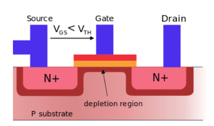
How does a MOSFET dosimeter work?
The gate voltage creates an electric field, controlling the drain-source current.
Ionizing radiation generates electron-hole pairs in the SiO₂ layer.
Holes move to the SiO₂ interface and get trapped, altering the threshold voltage (VT).
A constant current (~50 µA) flows between the source and drain.
The required gate voltage is measured, and the change in VT is proportional to the absorbed radiation dose.
what is the change in VT proportional to?
the radiation dose
What are the challenges of using MOSFET dosimeters?
Dose response is not linear (increases with total absorbed dose).
Readings must be taken after a specified time due to charge trapping/releasing.
Sensitivity changes with bias voltage during irradiation.
Small size means packaging affects readings.
What are the key characteristics of MOSFET dosimeters?
Extremely small (~10 µm wide, 1 µm thick).
Sensitivity depends on gate bias voltage (e.g., at 100V: 5V/Gy).
Used for in vivo dosimetry (attachable or implantable).
Effective in high dose gradients.