Electronic Principles, Diodes & Transistors (3b)
1/17
There's no tags or description
Looks like no tags are added yet.
Name | Mastery | Learn | Test | Matching | Spaced | Call with Kai |
|---|
No analytics yet
Send a link to your students to track their progress
18 Terms
What is a diode and what are its key functions?
A diode allows current to flow in one direction and blocks it in the opposite direction.
Terminals:
Anode = positive
Cathode = negative
Uses:
Early radio transmission
AC to DC conversion (power rectification) using rectifiers
Foundation for logic gates in computers
How is a diode constructed and what is its forward voltage behaviour?
Construction: P-type semiconductor + P-N junction (depletion region) + N-type semiconductor
Function: Conducts current from anode (P-side) to cathode (N-side), blocks reverse current
Forward voltage drop:
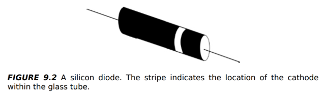
Silicon diode: 0.7 V
Germanium diode: 0.3 V
Diode acts as an insulator until this voltage is exceeded → then it is “turned on”
Bias direction: Current flows in the allowed direction
Recovery time: Time needed to overcome the forward voltage drop
What is diode bias, and what limits its reverse voltage?
Bias: Direction of applied voltage (forward or reverse)
Current flow: Anode (a, positive) → Cathode (k, negative) flows easily; reverse is blocked
Forward voltage drop: Diode acts as an insulator until exceeded
Reverse bias: Diode blocks current until Peak Inverse Voltage (PIV) is exceeded
Breakdown: Occurs if reverse voltage exceeds PIV, allowing electrons to overwhelm the P-N junction
Typical PIV values: 50V or higher
What is a Zener diode and how does it work?
A diode that conducts in reverse when a precise PIV is reached
Acts as a voltage-dependent switch or constant voltage diode
Type of avalanche diode (reverse current triggered by voltage surge)
Uses: Surge protection, voltage regulation
Usually paired with a resistor to limit current and prevent exceeding maximum ratings
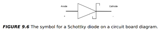
What is a Schottky diode and what are its key characteristics?
Construction: Metal + metal-oxide film attached to an N-type semiconductor
Features:
Very low forward voltage drop (0.15–0.45 V)
Fast recovery time
Uses: Power rectifiers, radio-frequency circuits, and other specialised applications
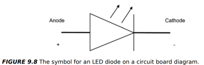
What is an LED and how does it work?
P-N junction diode made of direct band-gap materials
Operation: Electrons combine with holes → photon emitted (light)
Color: Determined by semiconductor material
White light: Combination of coloured or phosphor coating
Uses: Efficient lighting, infrared for remote controls
Circuit connection:
Series: Efficient for powering multiple from one source
Parallel: Requires individual resistors for each
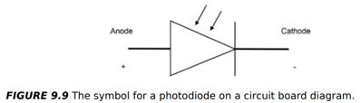
What is a photodiode and how does it work?
Photodiode: A diode designed to detect light
Unlike other diodes, its P-N junction is exposed to light
Structure:
PIN: P-type, Intrinsic, N-type
NIP: N-type, Intrinsic, P-type
Intrinsic semiconductor (I-type): Electrons excited via thermal energy or crystal defects
Applications: Optical storage, telecommunications, photography, and other light-sensing electronics
What is a transistor and what are its main types?
An electronic component that amplifies signals or acts as a switch
Function: Controls the amount and direction of current in a circuit
Main types:
Bipolar Junction Transistors (BJTs)
Field Effect Transistors (FETs)
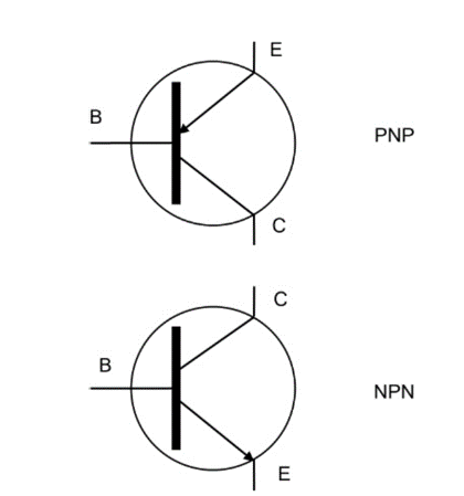
What is a Bipolar Junction Transistor (BJT) and how does it differ from diodes?
Essentially two diodes put end to end, but does not act as an insulator in both directions
Leads:
Collector (C): analogous to diode anode
Emitter (E): analogous to diode cathode
Base (B): third lead that controls current flow
Types: PNP and NPN, construction determines current direction and operation
What is the difference between PNP and NPN BJTs?
PNP BJT:
Collector & emitter = positive regions (excess holes)
Depletion region = negative (excess electrons)
Base-emitter junction: reverse-biased
Base-collector junction: forward-biased
NPN BJT:
Collector & emitter = negative regions (excess electrons)
Depletion region = positive (excess holes)
Base-emitter junction: forward-biased
Base-collector junction: reverse-biased
Base voltage controls current flow through the transistor
How does a BJT amplifier work?
Voltages applied to the collector and base control current flow.
Electrons flow through the transistor by combining with holes, creating new holes behind them.
Base voltage regulates this process, allowing amplification.
In an NPN BJT:
Majority carriers = electrons (negative regions)
Minority carriers = holes (positive region)
Current in the direction of majority carriers thins the depletion zone → faster electron transmission → amplified output
How do voltage levels affect a BJT’s operation?
Let VBV_BVB = base voltage, VCV_CVC = collector voltage, VEV_EVE = emitter voltage:
VE < VB < VC: Transistor acts as an amplifier
VE < VB > VC: Transistor acts as a conductor
VC > VB < VE: Transistor acts as an open switch (cuts off current flow)
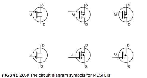
What is a Field Effect Transistor (FET) and how does it work?
FET Terminals:
Gate (G): Controls current flow, analogous to BJT base
Drain (D): Collects current, analogous to BJT collector
Source (S): Supplies current, analogous to BJT emitter
Body (B): Substrate of the transistor
Operation: Gate voltage opens/closes the channel between source and drain, controlling current flow
What are the types of FETs and their classifications?
General types:
Enhancement mode
Depletion mode
Further classification:
Bias type: N-channel or P-channel
Material or function-based
MOSFET (Metal-Oxide Semiconductor FET): Commonly used in digital logic gates
What is a schematic diagram and what are its key points?
Schematic diagram: Simplified graphical representation of a circuit, showing connections rather than physical appearance.
Key points:
Wires = straight lines
Junctions = dots
Components labelled (R1, C1, L1, etc.)
Current direction and voltage polarity clearly marked
What is a series circuit and how is total resistance calculated?
Series circuit: Components connected end to end
Current: Same through all components
Total resistance:
Rtotal=R1+R2+R3+…R_\text{total} = R_1 + R_2 + R_3 + \dotsRtotal=R1+R2+R3+…
What is a parallel circuit and how is total resistance calculated?
Parallel circuit: Components connected across the same voltage source
Voltage: Same across each branch
What is a mixed circuit?
A circuit that combines series and parallel connections of components