CSE 12 Midterm 1 Key Information
1/97
There's no tags or description
Looks like no tags are added yet.
Name | Mastery | Learn | Test | Matching | Spaced | Call with Kai |
|---|
No analytics yet
Send a link to your students to track their progress
98 Terms
Voltage
Unit: Volts (V)
—> The potential difference between ends of the circuit
Current
Unit: Amperes (Amps) (A)
—> The rate of flow of the electrons in a circuit
Resistance
Unit: Ohms (Ω)
—> Resistance the flow of electrons must overcome
Electrical Charge
Unit: Coulomb (C)
—> the amount of electricity conveyed in the circuit by one ampere,
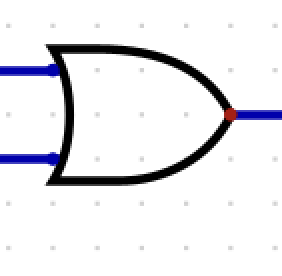
What is this?
OR
A + B
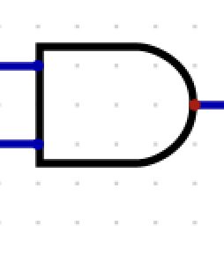
What is this?
AND
AB
What is this?
Inverter
A’
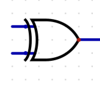
What is this?
XOR (Exclusive OR)
(A + B) * (AB)’
What is this?
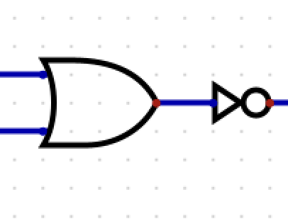
NOR
(A+B)’
A’B’
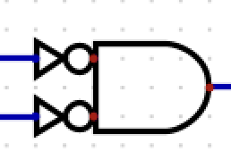
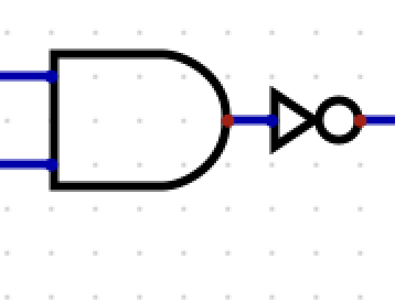
What is this?
NAND
(AB)’
A’ + B’

Vdd
Maximum voltage in the circuit
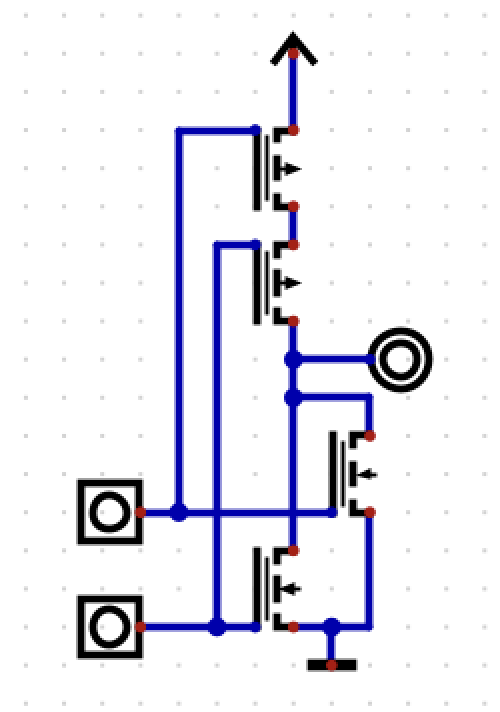
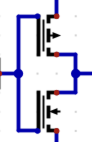
Switches in parallel
OR (PMOS)
NOR (CMOS) Shown in the image
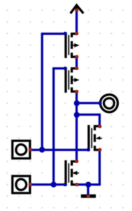
Switches in series
AND (PMOS)
NAND (CMOS)

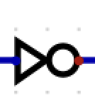
What is this?
PMOS “NOT”
In: 1 —> 0
In: 0 —> 1
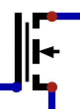
What is this?
NMOS “TRUE”
In: 1 —> 1
In: 0 —> 0
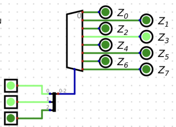
What is this?
Decoder: n inputs, 2n outputs of all minterms (combinations of inputs)
Used to:
1) generate a “one hot vector”: minterm where ONLY one bit is 1.
2) Converts memory or registers an address to a control line
3) Converts an opcode to n control lines (numerical representation of a command)
Section lines / Control lines
Number: log2(n) of the multiplexer’s inputs
input lines “conditional inputs” needed to narrow the n inputs to one output in a multiplexer
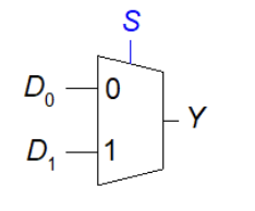
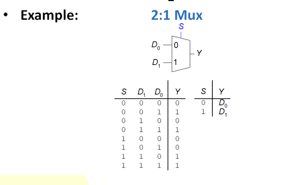
What is this?
Multiplexer
Outputs log2(n) bit-long output from n-bit inputs
Selects one of n inputs to send to control lines
Possibility to encode more than one input value into a multi-bit output value.
Minterm
Product that includes all the inputs (inverses of inputs are fine)
A term in the sum of products
ex. Inputs A,B,C
Minterms: ABC, A’BC, A’B’C, A’B’C’, ABC’, etc.
Maxterm
Sum that includes all the inputs (a term in the product of sums).
Multiplexer implementations
1) 2-Level: using AND, NOT, and OR gates to get a single output out of n inputs.
2) Tristate: Using tristate to select one of many inputs to send to an output.
3) Hierarchical: Using 2:1 multiplexers to simplify n to log2(n), use 2:1 multiplexers on next in series to simplify to one output at the end.
Sum of Products
Depicts all possible values of the inputs that are outputted as 1 (TRUE).
Used for NMOS sides of CMOS gates.
1) Look at truth table, find lines with TRUE as their output
2) take the product of all the inputs for each line.
3) Sum the products.
Product of Sums
AND combination of all the inverses of the terms (and combos) that would yield a zero.
The PMOS reflection of a true combination.
1) Find the rows with zero (FALSE) outputs
2) For each row, sum the invested of every single input in that line.
3) AND multiply the sums for the product of the sums.
Axiom Dual
For any axiom: Replace * with + and A with A’ (or vice versa)
B = 0 if:
B = 0 if B ≠ 1
0 * 0 =
0 * 0 = 0
Dual: 1+1 = 1
1*1 =
1*1 =1
“AND” gate
Dual:
0 + 0 = 0
0*1=
0*1 = 1*0 = 0
“OR” gate
Dual:
0+1 = 1+0 = 1
B * 1 =
B * 1 = B
Dual:
B+0 = B
B*B =
B* B = B
Dual:
B + B = B
(B’)’ =
(B’)’ = B
B*B’ =
B*B’ = 0
Dual:
B + B’ = 1
BC =
BC = CB
Dual:
B+C = C+B
(BC)D =
(BC)D = B(CD)
Dual:
(B+C)+D = B+(C+D)
B*(C+D) =
B*(C+D) = BC + BD
Dual:
B+(CD) = (B+C)(B+D)
B * (B+C) =
B * (B+C) = B
Dual:
B+(BC) = B
BC + BC’ =
BC + BC’ = B
Dual:
(B+C)*(B+C’) = B
DeMorgan’s Theorem
Key to any CMOS construction: a PMOS (PUN) / NMOS(PDN) and its dual.
(ABC)’ = A’ + B’ + C’
(A+B+C)’ = A’B’C’
Why is CMOS more popular than NMOS or PMOS?
CMOS is always connected to either ground or Vdd — AT NO POINT is there a current buildup on a single resistor —> Less overheating.
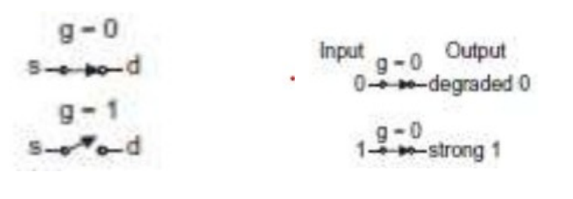
Floating Outputs / Floating Nodes
Denoted by Z
Might be 1, 0, or in-between 1 and 0 volts.
Caused by resistance in the circuit stripping away magnitude from Vdd.
—> Voltmeter’s DON’T DETECT Floating outputs/nodes.
—> Used for Tri-state Busses (Delivering one or more bits from one output node to several receiving nodes)
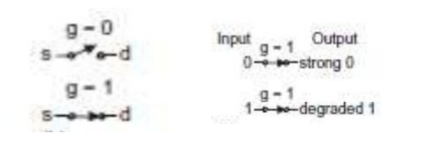
What is this?
NMOS Pass Gate
(Non positive feedback loop/ “non-regenerative”)
What is this?
PMOS Pass Gate
(Non-positive feedback loop/ “Non-regenerative”)
What is this?
Full Transmission Gate
Non-regenerative (no positive feedback loop)
No voltage threshold loss (same principle as CMOS)
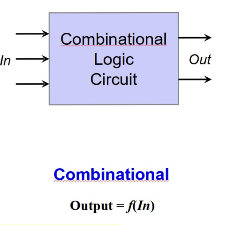
Combinational Logic Circuit
Circuit with no memory capability (no positive feedback looping), a “Stateless” machine.
Same out put for given set of inputs
Ex. Adder with Carry out and Sum out.
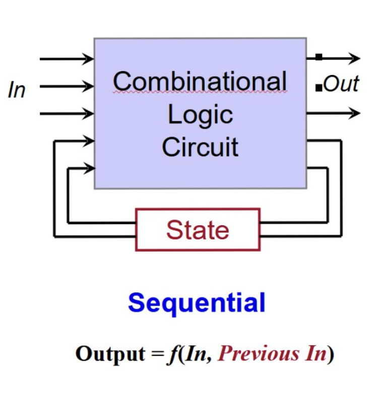
Sequential Logic Circuit
Circuit with feedback looping or “State” machines
Output depends on a SEQUENCE of inputs (past and present)
“Remembers” inputs previously with its “state”
NOTE: Alternative way to store memory w/o positive feedback loop: Capacitor storing charge
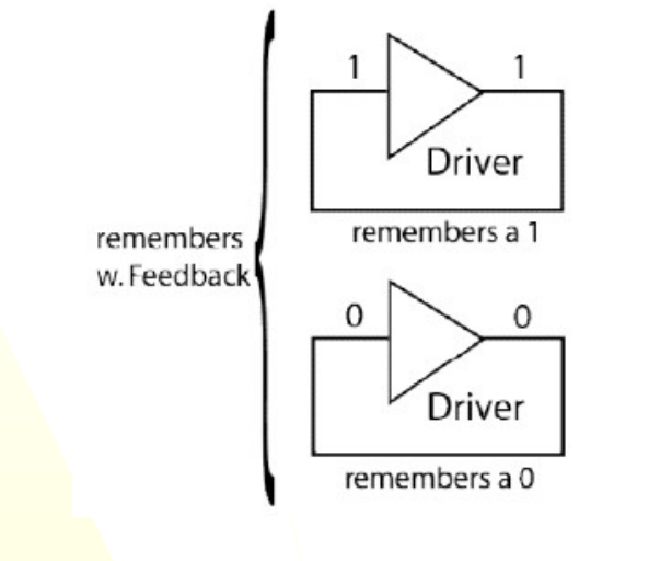
How do state machines work? How can you cell the function of a state machine?
Driver in a loop with itself ie. output of the driver goes to the input of the driver
The driver keeps repeating the inputted signal to itself before it is referenced again.
CANCELLING: Driver + inverter —> the signal flips every time it is repeated into the driver and the original signal is lost.
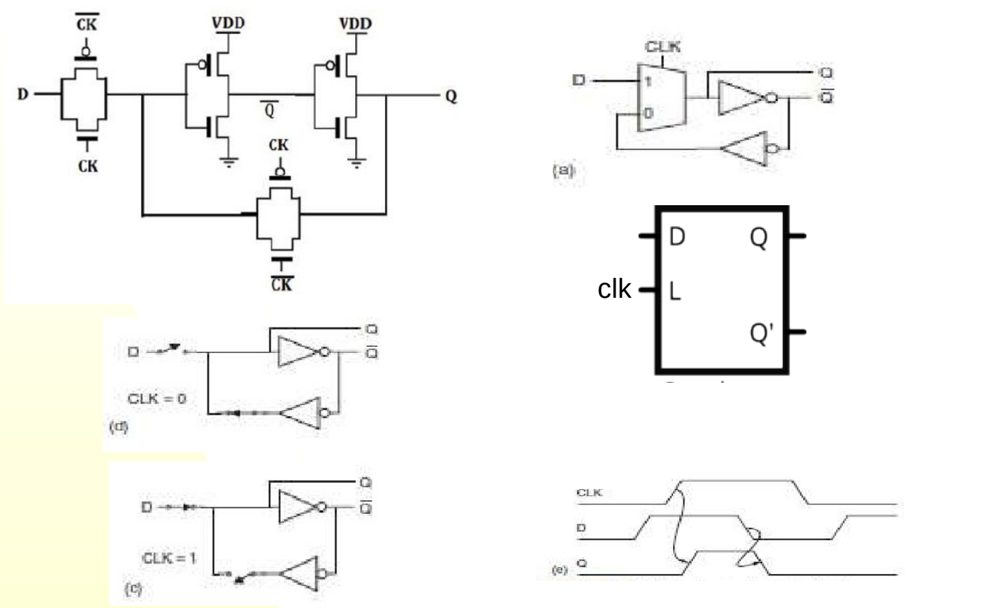
What is this?
See-through D-latch:
When the enable signal is 1, allows input d to go directly to output Q (hence the “See-through”)
When enable signal is 0, it “remembers” the last d value when enable was 1 and sends that to output Q.
What is this?
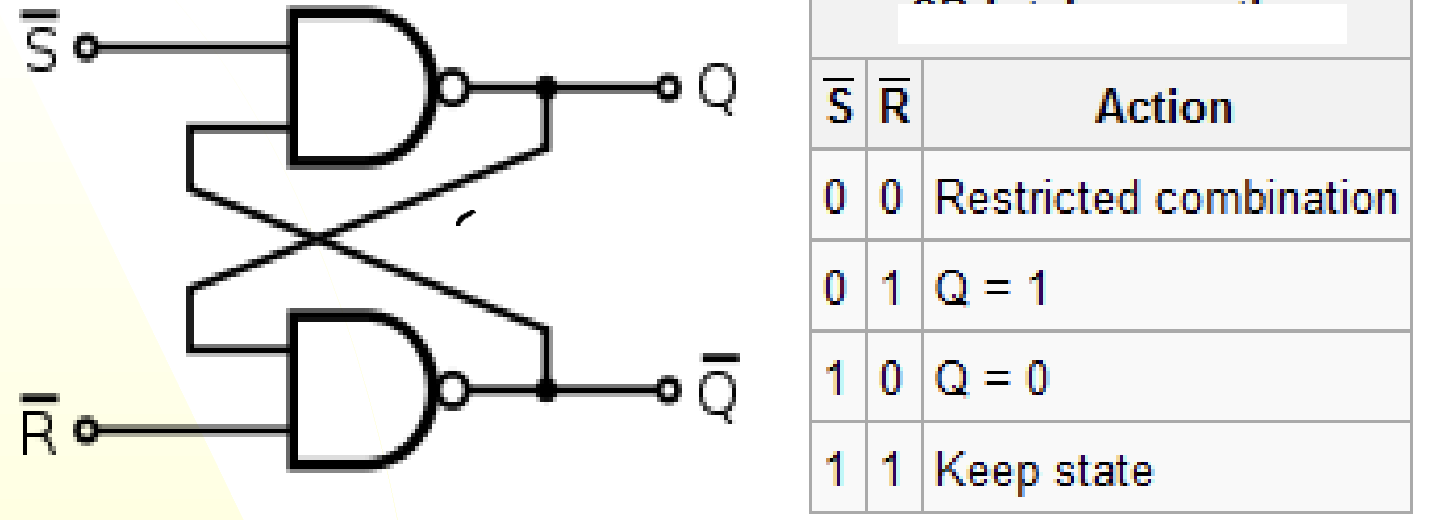
NAND SR Latch (“Set-reset latch”)
One input controls whether the value is set. (S)
The other controls whether the value is cleared. (R)
S = 0, R = 0 is an undefined output (non-functional)
S = 1, R = 1 keeps the state of the input.
SR’ —> Q = 1 or S’R —> Q = 0
What is this?
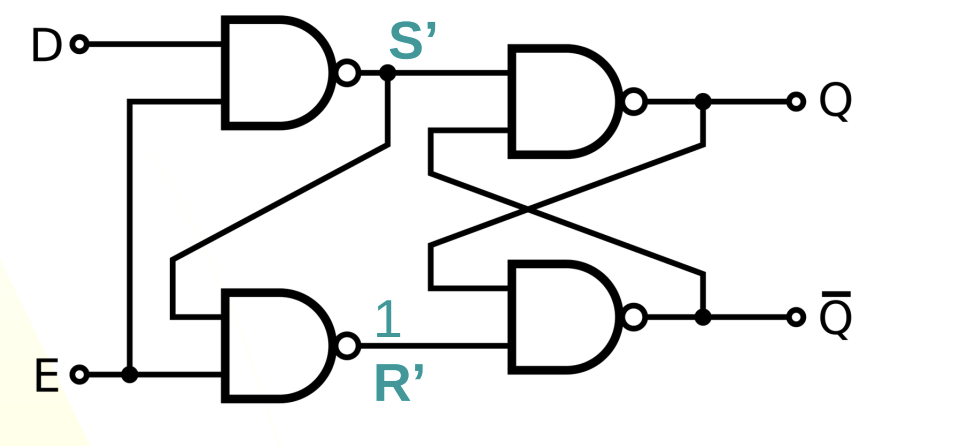
SR NAND D-Latch
Resets to D when E = 1, else it retains its previous value.
What is this?
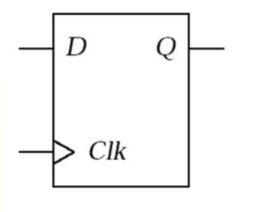
Positive edge-triggered Flip-flop
TRIANGLE IMPLIES EDGE TRIGGERED
When the Clock (Ck, the eval input) goes from 0—>1, then the system resets as D.
In ANY other circumstance, the flop does not flip.
EASY TO USE compared to see-thru gates (edge input is the only variable, D can be handled separately.)
What is this?
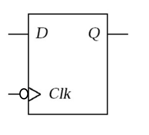
Negative edge-triggered D flip-flop:
when the clock (eval edge labeled “clk”) goes from 1—>0, the stored data is reset to D and then looped until the next “falling” edge.
NO OTHER clk inputs will make it change.
What is this?
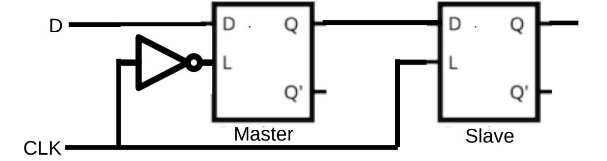
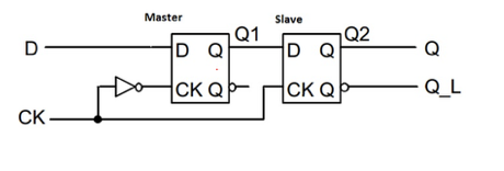
Positive edge-triggered latch
When the Clk = 1, signal is immediately passed through D to Q
Else, the D see-through latch locks.
“master” clock controls flow, “Slave” clock controls D.
“MASTER” clock: positive clock, “SLAVE” clock: negative clock
What is this?
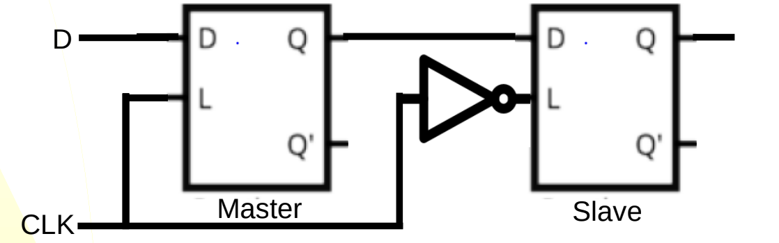
Negative edge-triggered D-latch
Circuit is completed ONLY when Clk goes to 0
Else, it is locked.
“master” clock controls flow, “slave” clock controls D.
“MASTER” Clock: negative clock, “SLAVE” clock: negative clock.
What is this?
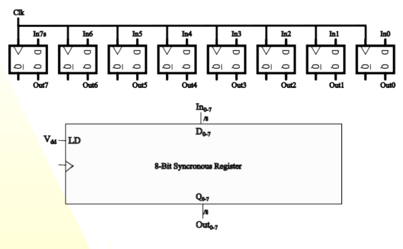
Synchronous register
Allows for parallel processing of the data (Registers can only store one bit, synchronizing registers gives the ability to process more than one bit).
Uses a clock to synchronize (time and work together) operations on bits.
Type of Shift register (because positive-shift or negative-shift edge register)
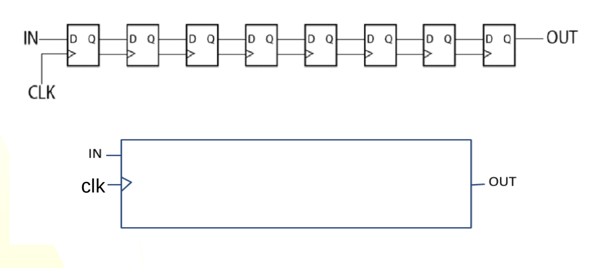
What is this?
Synchronous Register
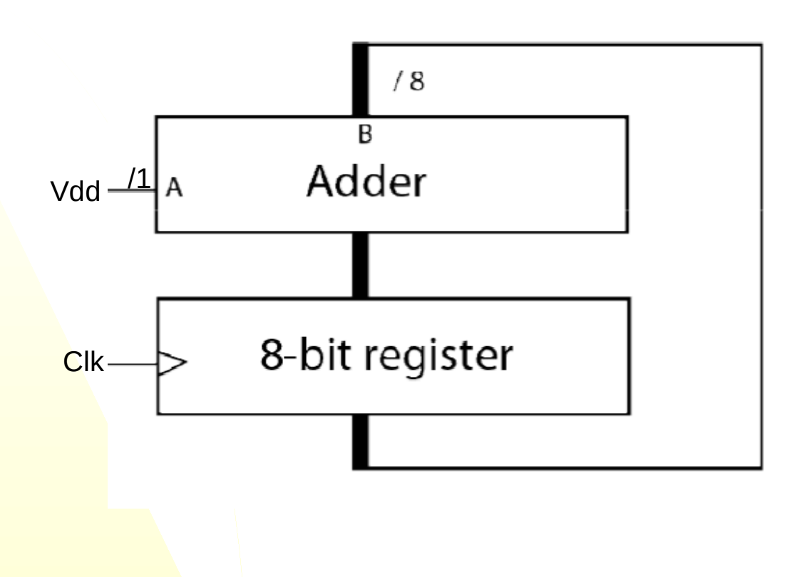
What is this?
A counter
Increments or decrements a saved (registered) value according to the pulses of the clock.
Binary
Base-2 language of computers
only 1 or 0 for 1 volt or 0 volt across recievers
combinations of 101-strings to convey complex data to registers.
Bit
1 digit of the binary string
2 possibilities: 0 or 1
KEY: 2n possible arrangements of n bits
Byte
8 bits
Number of bits of storage (characters, numbers, addresses)
Chars: 8-16 bits: 2³- 2^4 bits
Numbers: 32-64 bits: 2^5 - 2^6 bits
addresses: 32-64 bits: 2^5 - 2^6 bits
Integer representations
1) Unsigned integers
2) One’s complement (Archaic)
3) Two’s complement
Unsigned integers
Represents ONLY positive integer values in BINARY.
Records up to 2n-1 distinct values (one place being saved for the zero value, ie. zero indexing.)
Signed integers
Positive and negative values encoded in the number IN BINARY.
One bit represents the sign (this is the “most significant bit (MSB)”):
MSB = 0 → +
MSB = 1 → -
Range: -(2n-1) to 2n-1
Additive Inverse
Invert the sign bit on a signed integer.
One’s complement
Archaic
Negation of the positive signed numbers, inverting all bits on the positive unsigned version of that number
Wastes a bit value because there is a positive and negative zero with this system.
The top bit is the MSB or “sign bit”
All other bits are magnitude.
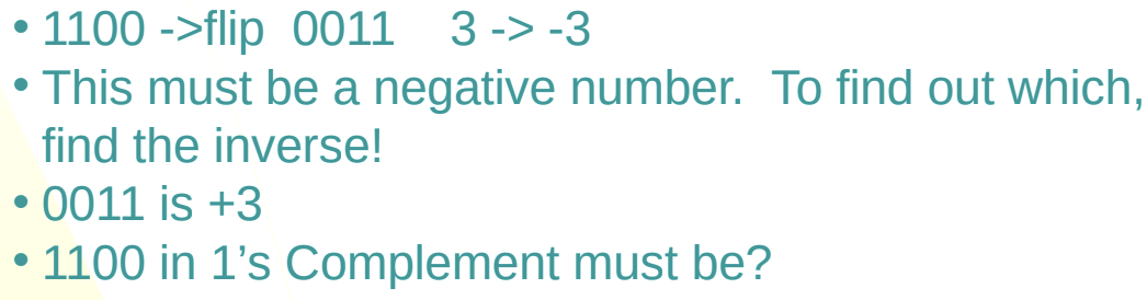
Two’s complement
Represents positive and negative signed integers
Range: -2n-1 to 2n-1
NOTE: largest negative number in 2’s complement bit range can’t be converted to positive in that bit range. (this is the “integer overflow” condition)
Does not contain negative zero, saving machinery compared to 1’s complement.
Positive: positive unsigned binary number, same as ever
Negative (converting to binary and evaluating binary): invert all bits of the positive number, add one to the new binary number.
ADDITIVE INVERSE (negation): One’s complement of the number, add one.
Sign Extension
Increasing the number of bits, but keeping the binary value those bits represent and their signs.
Makes processing work with registers of different sizes.
Process: add 0 bits in between the MSG and binary magnitude representation until the number of bits is satisfied.
Ex. 0001 = 1 in 4-bit, 00000001 = 1 in 8-bit
Ex. 1001 = -6 in 4-bit 2’s complement, 111110001 = -6 in 8-bit 2’s complement
Bitwise Logical operations
NOT the same as Language logical operations.
Language logical operations are performed on explicit boolean values (true, false)
These are used for binary numbers and the like.
Done IN PARALLEL with corresponding bits in the data.
Bitwise NOT
~
ex. ~101 = 010
Bitwise AND
&
Ex. 0011 & 1010 = 0010
Bitwise OR
|
ex. 0011|1010 = 1011
Bitwise XOR
^
ex. 0011^1010 = 1001
Binary Addition
Like decimal addition. Carry the 1’s over to the next exponent place if the limit in one sections reached.
Implemented:
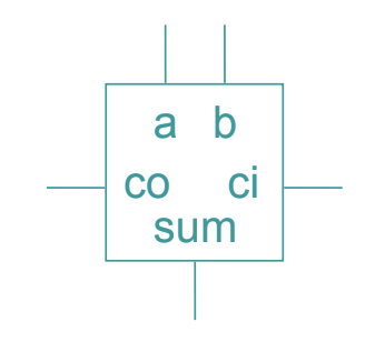
Full adder cells.
3 inputs: Carry-in (for carrying into the addition from the last bits), a (input number 1), b (input number 2)
2 outputs: Sum (total number), Carry-out (if there’s a carry to the next highest bit)
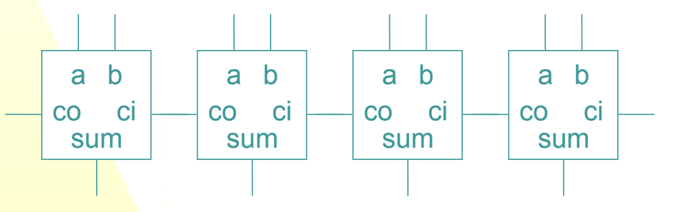
What is this?
Ripple-Carry adder
full-adders pass along the carryout into the carrying for the next adder (wired in series because all must be passed through)
time taken proportional to number of bits (LOTS of time)
What is this?
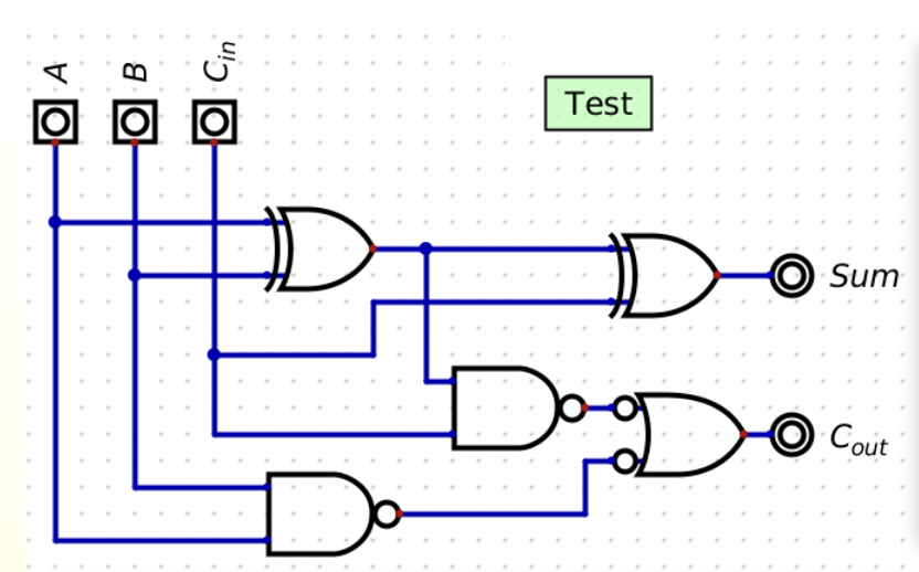
Full adder
Calculates the sum of two binary numbers in binary
3 inputs, 2 outputs
Sum = A xor B xor Cin, Cout = Majority(A,B,Cin)
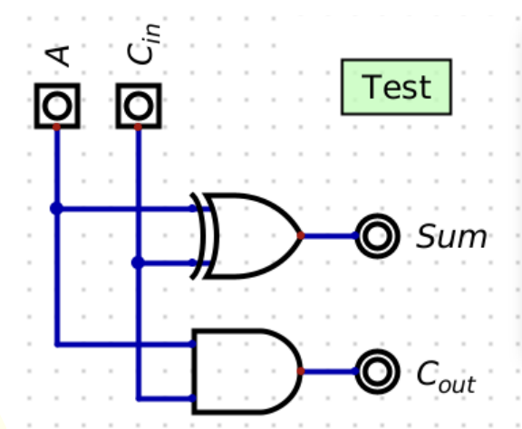
What is this?
Half-Adder
Used for counting up by increments of 1.
Sum = A xor Cin, Cout = A and Cin
Adding in Binary
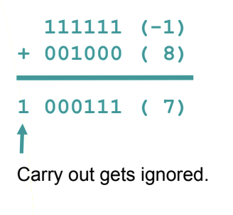
1) Unsigned: no issue, like standard addition (The carry-out IS KEPT as the “leading” number of the binary sequence ON TOP OF the resultant sum.)
2) SIGNED, 2’s complement: same as unsigned addition, BUT ignore the carry-outs on the very end if it doesn’t fit within the bit number. (see image)
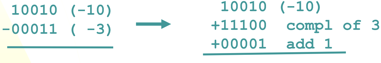
Subtraction in Binary
Treat the subtractant in 2’s complement (fully make it negative), then add the two numbers.
If there’s a carry beyond the total number of bits, ignore it (for SIGNED AND UNSIGNED SUBTRACTION)
Binary
Base 2 (0-1)
Octal
Base 8 (0-7)
Binary to Octal: Group binary starting at far right into groups of 3. Evaluate those groups of 3. The result is your number in octal.
Octal to binary: split each octal bit into three binary bit representations of that octal bit’s number.
Hexadecimal (hex)
Base 16 (0-9, A-F)
Binary to hex: Group the binary from far right to let in groups of four. evaluate those groups of 4. what remains is the number in hex.
hex to binary: split each hex number into its representation in 4-bits of binary.
Used to represent color values in RGB GUIs.
Used to create a multi-valued truth table.
Shifts
Operations moving bits to the right or left.
Logical Shifts
Treat operands like unsigned numbers. Do nothing to the signed bit, except include it in the move.
In effect, dividing (or multiplying) by powers of 2
Moves terms n times to the right or left, preserve order and pattern unless “fallen” off of the right side or “fallen” off the left side.
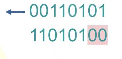
Replace space shifted rightward on the far left hand side with 0s, or space shifted leftward with 0s. (Logical shift left, see image)
Arithmetic shifts
Operations shifting according to the sign bit and sign extension.
In effect, dividing (or multiplying) a signed number by powers of 2.
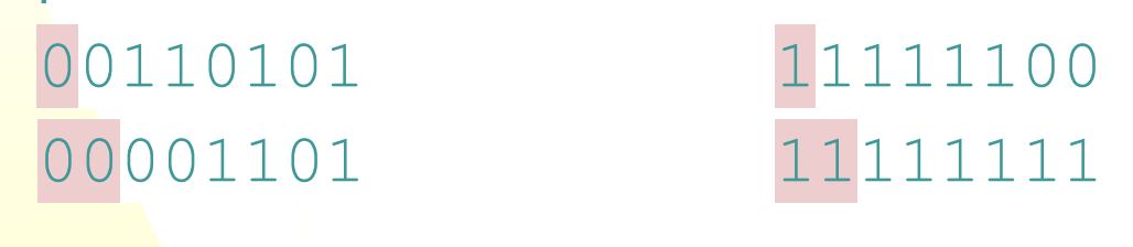
RIGHT: Preserve order and pattern of the original number and shift n place to the right. If digits “fall off” the right side, ignore it.
—> Fill the space left over from the shift with the MSB’s indicated sign of the number.
LEFT: Preserve order and pattern of the original number and shift n places to the left. If digits" “fall off” the left, ignore it.
—> Fill the space left over from the shift with 0s.
NOTE: LEFT shifting has the chance to create overflows.
—> python: rounds toward negative infinity if remainder left over in integer division
—> C: truncates towards 0 if remainder left over in integer division.
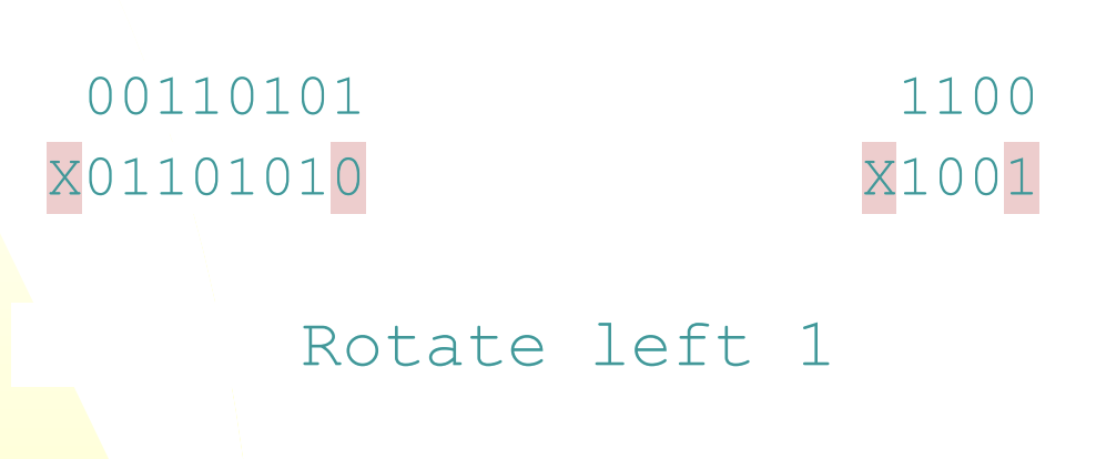
Rotations
Move data from one end to the other.
Treat operands being rotated as unsigned
MSB is not treated with any special regard
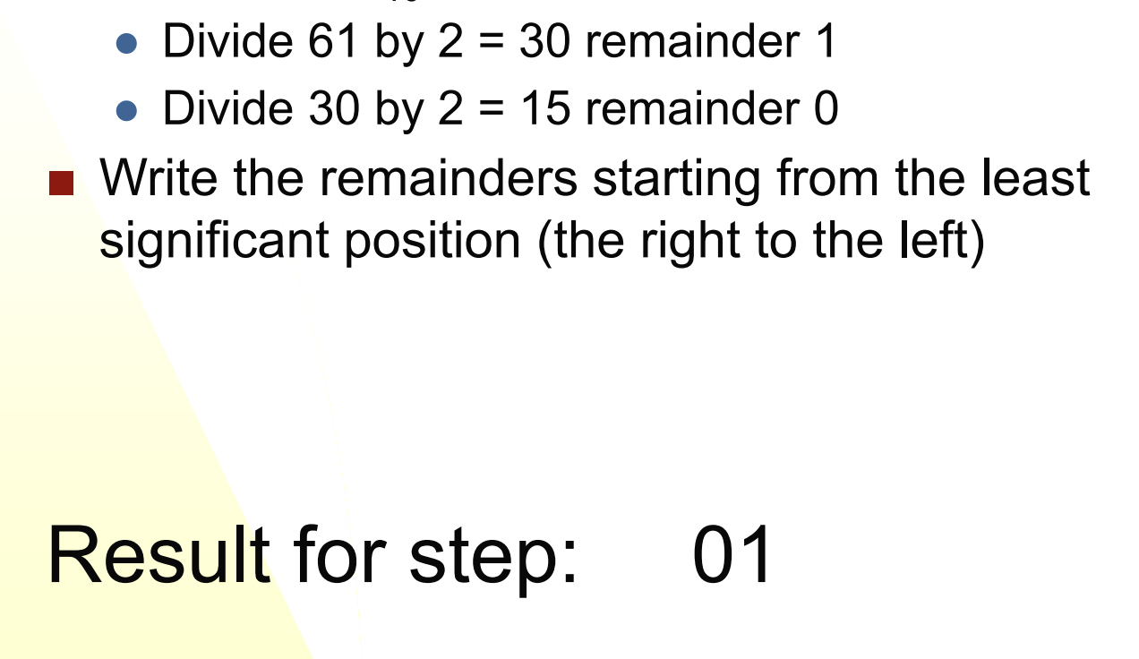
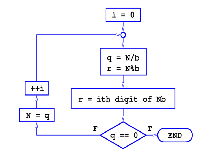
Decimal to Binary
Use repeated divisions
Divide the decimal number by 2 —> record the remainder of this
keep dividing by 2 until the quotient is 0. Write the remainders in reverse order (remainder gotten last at the far left and remainder gotten first at the right). this is your binary number.
Any base to any base
Convert from the first base to base ten, then the base ten to the desired second base.
How many bits are necessary to express a number n in base b?
logb (n) bits are needed
ie. (log(n)/log(b)) bits are needed.
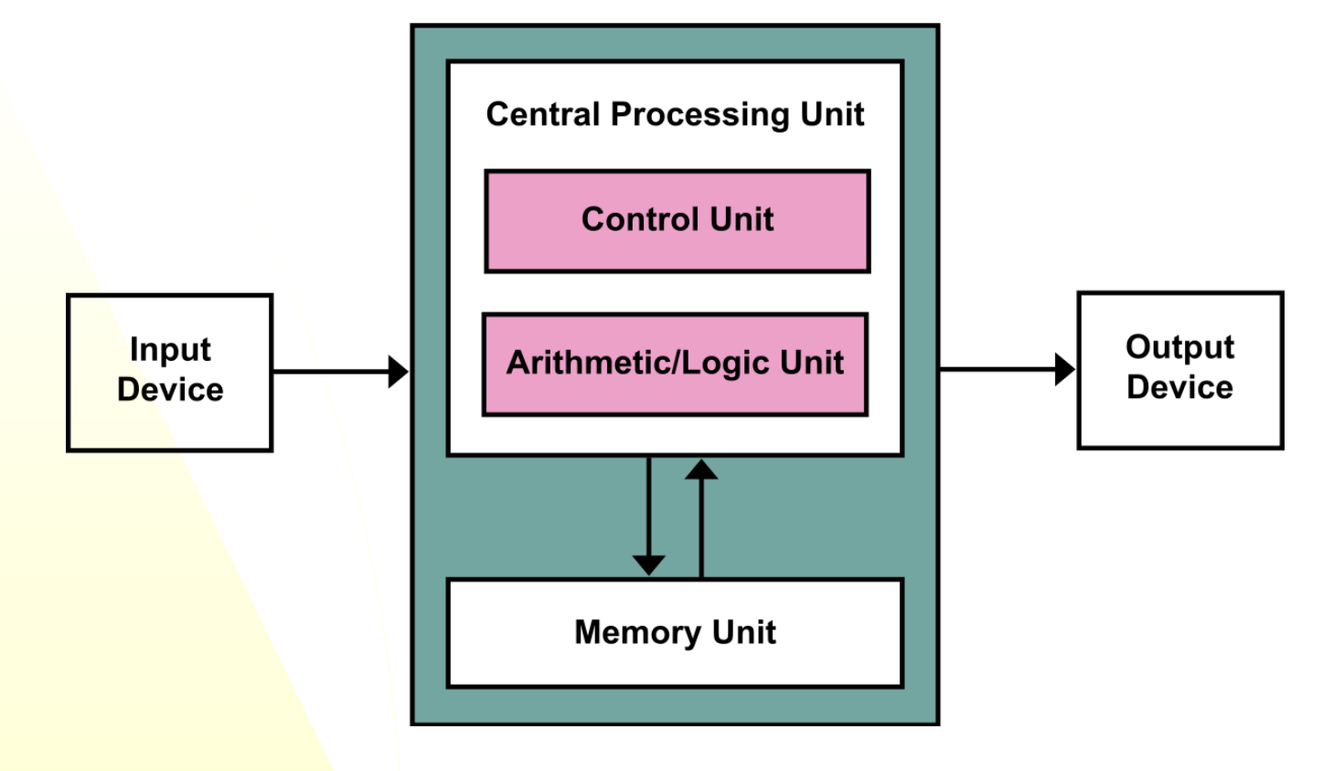
What is this?
The Von Neumann Model
CPU
Computer Processing unit
RALU (Register Arithmetic Logic Unit)
Arithmetic and logic unit (ALU)
General Purpose Registers (GPRs)
—> Control unit
Program counter
Branching Logic
Instruction register
Stored programs
The backbone of every computer theory; a set of instructions and executables that can be stored in a computer’s memory.
CPU Memory
Stores Data, program instructions (a set of 1s and 0s that is 32 bits is RISC-V)
GPRs are temporary storage for data being processed but the ALU.
NOTE: MAIN MEMORY IS NOT IN THE CPU
Main Memory
Ultimate destination and origin of data and instructions
Addresses
Data in the main memory is referred to by its addresses (within directories and subdirectories of the memory)
“Bit patterns that uniquely identify the location of a memory”
Contents: Bit pattern stored at that address
Number of bytes in a word
4 bytes (32 bits)
Addressability
Number of bytes of memory being called at a certain address.
RISC-V is byte addressable.
Overflow in addition
When in addition operations causes the signs to change unreasonably; ie. binary adding two negative 2’s complements results in a positive 2’s complement, (or adding two positives and getting a negative result) this is “overflow” and is not a valid addition result.
What is this?
Positive-Triggered D flip-flop
Sequential Circuit
(NOTE: 2 d see-throughs is a d flip-flop circuit)