Semiconductor Devices and Sensors
1/72
There's no tags or description
Looks like no tags are added yet.
Name | Mastery | Learn | Test | Matching | Spaced | Call with Kai |
|---|
No analytics yet
Send a link to your students to track their progress
73 Terms
On what factors are semiconductors classified and why is it important?
They are classified based on Nature of the energy band gap and
Relative positions of the CB Min & VB Max in energy (E) vs wave vector (k)
They are classified into Direct Band Gap SCs and Indirect BG SCs.
It is important because it determines the optical and electronic properties of semiconductors
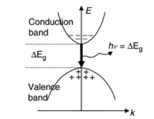
What are Direct Band Gap Semiconductors?
A direct band gap semiconductor is one in which the minimum of the conduction band and the maximum of the valence band occur at the same value of wave vector (k).
Explain the E-k Diagram of Direct Band Gap Semiconductors
• In the E–k diagram, both CBM and VBM lie vertically above each other. (aligned)
• Electron transition from valence band to conduction band does not require change in momentum.
• Energy transition occurs directly by absorption or emission of a photon.
What are the Characteristics of a Direct Band Gap Semiconductor?
• High probability of radiative recombination
• Efficient light emission
• Strong optical absorption and emission
List some examples of Direct Band Gap Semiconductors
• Gallium Arsenide (GaAs)
• Indium Phosphide (InP)
• Cadmium Sulphide (CdS)
• Gallium Nitride (GaN)
List some applications of Direct Band Gap Semiconductors
• Light Emitting Diodes (LEDs)
• Laser diodes
• Optoelectronic devices
• Solar cells (high efficiency)
What are Indirect Band Gap Semiconductors?
An indirect band gap semiconductor is one in which the conduction band minimum and valence band maximum occur at different values of wave vector (k).
Explain the E-k Diagram of Indirect Band Gap Semiconductors
In the E–k diagram, CBM and VBM are not aligned vertically.
Electron transition requires:
A photon for energy
A phonon for momentum conservation
Hence, transition probability is lower.
What are the Characteristics of a Indirect Band Gap Semiconductor?
• Low probability of radiative recombination
• Poor light emission
• More suitable for electronic than optical devices
List some examples of Indirect Band Gap Semiconductors
• Silicon (Si)
• Germanium (Ge)
• Silicon Carbide (SiC)
List some applications of Indirect Band Gap Semiconductors
• Transistors
• Integrated circuits
• Diodes
• Power electronic devices
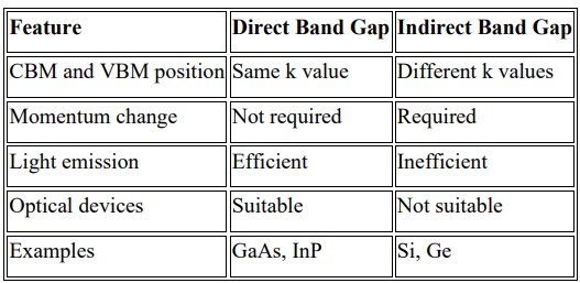
Compare Direct and Indirect Band Gap Semiconductors
What is a Semi-conductor Laser?
A semi-conductor diode laser is a specially fabricated PN junction device that emits coherent light when it is forward biased.
Explain the Construction of a Semi-conductor Laser
The diode is extremely small in size with sides of the order of 1 mm.
The junction lies in a horizontal plane through the center with thickness 1 μm.
A pair of parallel planes are cleaved or polished perpendicular to the plane of the junction.
The two end faces are polished (cleaved) so that they act as mirrors. The photons are reflected back and forth between these mirrors through the active region.
The top and bottom faces are roughened to prevent lasing action in that direction.
The top and bottom surfaces are roughened, so light travelling in those directions is scattered and cannot undergo repeated reflections. This prevents laser action in the vertical direction.
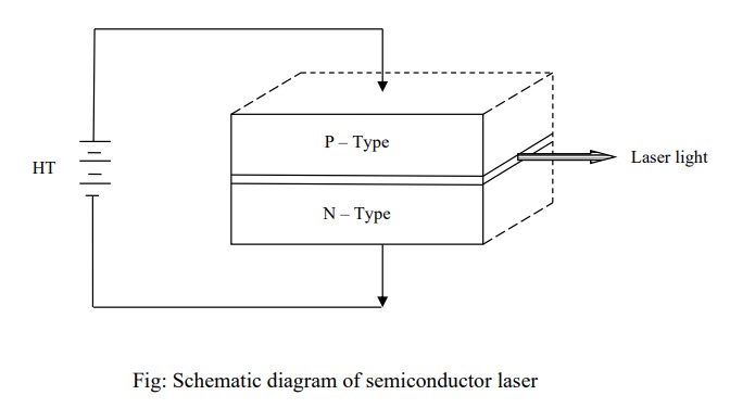
Explain the working of a Semi-conductor Laser
When a forward bias is applied to the semiconductor, perpendicular to the plane of the junction a forward current flows.
As the bias is increased, eventually a threshold current is reached
at which the stimulated emissions occur and a monochromatic and highly directional beam of light is emitted from the junction
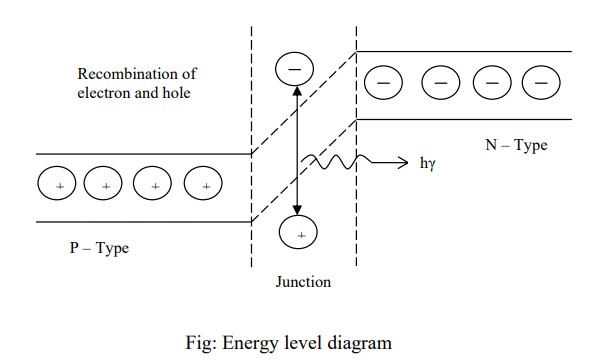
Simplify the Working of a Semiconductor laser
A forward bias is applied to the heavily doped PN junction.
Electrons move from the N-region and holes move from the P-region toward the junction.
The conventional current flows from the P-region to the N-region.
They recombine in the active region.
Initially, spontaneous emission produces photons.
The top and bottom surfaces are roughened, so light travelling in those directions is scattered and cannot undergo repeated reflections. This prevents laser action in the vertical direction.
The two end faces are polished (cleaved) so that they act as mirrors. The photons are reflected back and forth between these mirrors through the active region or junction.
When the forward current reaches the threshold current, the reflected photons cause stimulated emission.
The number of identical photons increases rapidly.
One polished face allows part of the amplified light to emerge as a coherent, monochromatic, highly directional laser beam.
What are the conditions to achieve laser action?
Conditions to achieve laser action are
We have to pass a large current
both P-type and N-type semiconductors are heavily doped
Because of large forward current a hole moves from the P to N side and an electron moves from N to P side.
At the junction a recombination of electron and holes takes place and the energy is released in the form of light, which is a stimulated radiation.
What are some advantages of Semiconductor Laser?
They are compact
They are efficient
They are highly stable
They can be easily fabricated
They are least expensive
What are photodiodes?
Photodiodes are semiconductor devices that respond to high-energy particles and photons.
Radiation-sensitive junction is formed in a semiconductor material whose resistivity changes when illuminated by light photons.
The junction can be made to respond to the entire electromagnetic spectrum
PN junction photodiodes comprise a two electrode, radiation-sensitive PN junction formed in a semiconductor material in which the reverse current varies with the amount of illumination.
What is an LDR?
A Light Dependent Resistor aka photoresistor, is a passive semiconductor device whose resistance varies with the intensity of incident light.
Its resistance decreases when light intensity increases and decreases in darkness.
LDRs work on the principle of photoconductivity.
How is LDR Constructed?
An LDR is made of photoconductive semiconductor material such as:
Cadmium Sulphide (CdS)
Cadmium Selenide (CdSe)
The material is deposited in a zigzag pattern on an insulating substrate to increase the effective length.
Metal electrodes are attached at both ends.
The assembly is enclosed in a transparent glass or plastic cover to allow light to fall on it.
Explain the Working Principle of LDR
Photoconductivity
In darkness:
Very few free charge carriers are available.
Hence, the resistance is very high (typically in megaohms).
When light falls on the LDR:
Photons with energy greater than the band gap excite electrons from the valence band to the conduction band.
Number of free charge carriers increases.
Electrical conductivity increases and resistance decreases.
Thus, resistance is inversely proportional to light intensity.
What are the characteristics of LDR?
1. Resistance in dark: Very high (≈ 1–10 MΩ) 2. Resistance in bright light: Low (≈ 100–500 Ω) 3. Response time: Slow compared to photodiodes 4. Sensitivity: High for visible light 5. Temperature dependence: Resistance decreases with rise in temperature
List some Advantages of LDR
List some Disadvantages of LDR
List some applications of LDR
• Automatic street light control • Light intensity meters (lux meters) • Burglar and security alarm systems • Automatic brightness control in displays • Camera exposure control • Fire and smoke detection systems
What are RTDs?
A Resistance Temperature Detector (RTD) is a temperature-sensitive sensor that operates on the principle that the electrical resistance of a metal changes with temperature. RTDs are widely used for accurate and stable temperature measurement over a wide range of temperatures.
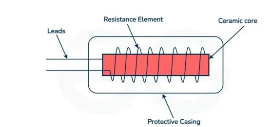
How is RTD constructed?
• RTD is made using pure metals such as: o Platinum (Pt) – most commonly used o Nickel (Ni) o Copper (Cu) • A fine metal wire is wound in a coil or deposited as a thin film on a ceramic or glass substrate. • The sensing element is enclosed in a protective sheath made of stainless steel or glass. • Electrical leads are connected using 2-wire, 3-wire, or 4-wire configurations to minimize lead resistance errors.
What are the types of RTD?
1. Wire-wound RTD o High accuracy o Used in precision measurements 2. Thin-film RTD o Small size o Faster response o Lower cost
Characteristics of RTD
Characteristics of RTD • High accuracy • Excellent stability and repeatability • Nearly linear resistance–temperature relation • Wide temperature range (–200°C to 850°C for platinum RTD) • Slow response compared to thermocouples
Advantages of RTD
• Very high measurement accuracy • Good long-term stability • High sensitivity • Suitable for industrial and laboratory use
Disadvantages of RTD
• Higher cost compared to thermistors • Slower response time • Requires external power supply • Lead wire resistance can introduce errors
Applications of RTD
• Industrial temperature monitoring and control • Power plants and chemical industries • Food processing industries • HVAC systems • Laboratory and calibration equipment • Medical instruments
Sensing Mechanisms
A sensing mechanism refers to the physical principle by which a sensor detects a change in a measurand (such as temperature, pressure, light, displacement, or gas concentration) and converts it into a usable electrical signal. The choice of sensing mechanism depends on accuracy, sensitivity, response time, and application requirements.
Major Sensing Mechanisms
Resistive Sensing Mechanism
• Based on the change in electrical resistance due to variation in a physical quantity. • The resistance changes according to: R=ρ L/A • Used in sensors where temperature, strain, or light affects resistivity. Examples: • Resistance Temperature Detectors (RTD) • Thermistors • Strain gauges • Light Dependent Resistor (LDR) Applications: • Temperature measurement • Pressure and strain sensing • Light intensity detection
2. Capacitive Sensing Mechanism
• Operates on the change in capacitance caused by variation in distance, area, or dielectric constant. • Capacitance: C=εA/d Examples: • Capacitive pressure sensors • Proximity sensors • Touch screens • Humidity sensors Applications: • Displacement measurement • Liquid level sensing • Touch-based devices
. Inductive Sensing Mechanism
• Based on the change in inductance due to movement of a magnetic core or conductive object. • Works on Faraday’s law of electromagnetic induction. Examples: • LVDT (Linear Variable Differential Transformer) • Eddy current sensors • Proximity sensorsApplications: • Position and displacement measurement • Speed sensing • Metal detection
Piezoelectric Sensing Mechanism
• Certain materials generate an electric charge when subjected to mechanical stress. • Known as the piezoelectric effect. Examples of materials: • Quartz • PZT (Lead Zirconate Titanate) Applications: • Vibration sensors • Accelerometers • Pressure and force sensors • Ultrasonic transducers
5. Optical (Photoelectric) Sensing Mechanism
• Based on interaction between light and matter. • Light intensity alters electrical properties of the sensing element. Types: • Photoconductive • Photoemissive • Photovoltaic Examples: • Photodiodes • Phototransistors • LDRs Applications: • Light meters • Optical encoders • Automatic lighting systems
6. Thermal Sensing Mechanism
• Operates based on temperature-dependent electrical properties. • Can use resistance change or thermoelectric effect. Examples: • Thermocouples (Seebeck effect) • RTDs • Thermistors Applications: • Industrial temperature control • Furnace monitoring • Medical thermometry
7. Magnetic Sensing Mechanism
7. Magnetic Sensing Mechanism • Based on changes in magnetic field or flux density. Examples: • Hall effect sensors • Magnetoresistive sensors Applications: • Speed and position sensing • Current measurement • Automotive sensors
Comparison Summary
Piezo-Electric Sensors
A piezo-electric sensor is a device that converts mechanical stress (force, pressure, vibration, or acceleration) into an electrical signal based on the piezo-electric effect. These sensors are widely used for dynamic measurements due to their high sensitivity and fast response.
Piezo-Electric Effect
The piezo-electric effect is the phenomenon in which certain crystalline materials generate an electric charge when subjected to mechanical stress. • Direct piezo-electric effect: Mechanical stress → Electrical charge (used in sensors) • Inverse piezo-electric effect: Electrical field → Mechanical deformation (used in actuators)
Piezo-Electric Materials
Common piezo-electric materials include: • Quartz • Rochelle salt • Barium titanate • Lead Zirconate Titanate (PZT) – most widely used
Construction of Piezo-Electric Sensor
• The sensor consists of a piezo-electric crystal sandwiched between two metallic electrodes. 20 • The assembly is mounted inside a protective casing. • When mechanical force is applied, charges appear on the crystal surfaces and are collected by electrodes. • The output is usually connected to a charge amplifier.
Working Princip
• When an external mechanical force or pressure is applied to the piezo-electric crystal: o The crystal lattice deforms. o Positive and negative charge centers separate. o An electric potential difference is developed across the electrodes. • The output voltage is proportional to the applied force. Q=d×F where: • Q = generated charge • d = piezo-electric constant • F = applied force
Characteristics of Piezo-Electric Sensors
• High sensitivity • Wide frequency range • Fast response time 21 • Small size and lightweight • High output voltage
Advantages • No external power supply required • High dynamic response • Wide operating temperature range • Rugged and reliable Disadvantages • Not suitable for static measurements • Output signal decays with time • Requires signal conditioning • Sensitive to temperature variations
Applications of Piezo-Electric Sensors
• Vibration and acceleration measurement • Pressure and force sensing • Acoustic sensors and microphones • Ultrasonic transducers • Knock sensors in automobiles • Structural health monitoring
Comparison with Other Sensors
• Compared to resistive sensors: faster response • Compared to capacitive sensors: better for dynamic forces • Compared to RTDs: not used for temperature sensing
Metal Oxide Semiconductor (MOS) Sensors
Metal Oxide Semiconductor (MOS) sensors are a class of chemical sensors used mainly for gas detection. They operate based on the change in electrical resistance of a metal oxide material when it interacts with surrounding gases. MOS sensors are widely used due to their high sensitivity, simple construction, and low cost.
Principle of Operation
MOS sensors work on the principle of surface-controlled conductivity. • When the sensor is exposed to air, oxygen molecules are adsorbed on the surface of the metal oxide. • These oxygen molecules trap free electrons, forming oxygen ions. • This creates a depletion layer near the surface and increases resistance. • When a target gas (reducing or oxidizing gas) comes in contact: o Reducing gases (CO, H₂, CH₄) react with adsorbed oxygen and release electrons. o This decreases resistance of the sensor. o Oxidizing gases increase resistance. Thus, the change in resistance is proportional to gas concentration
Construction of MOS Sensor
• Sensing Element: Metal oxide semiconductor such as: o Tin Oxide (SnO₂) o Zinc Oxide (ZnO) o Titanium Dioxide (TiO₂) • Heater Element: Maintains operating temperature (200–400°C). • Electrodes: Collect output signal. • Substrate: Ceramic or glass. • Protective Mesh: Allows gas diffusion and protects sensor.
Working Mechanism
1. Sensor is heated to operating temperature. 2. Oxygen adsorption creates an electron depletion layer. 3. Exposure to target gas changes surface chemistry. 4. Electrical resistance changes. 5. Resistance variation is converted into output signal.
Characteristics of MOS Sensors
• High sensitivity • Wide detection range • Fast response and recovery time • Long operational life • Operates at high temperature
Advantages of MOS Sensors
• Simple structure • Low manufacturing cost • High sensitivity to gases • Long lifespan • Suitable for continuous monitoring
Disadvantages of MOS Sensors
• High power consumption (due to heater) • Poor selectivity (responds to multiple gases) • Affected by humidity and temperature • Requires calibration
Applications of MOS Sensors
• Gas leakage detection (LPG, methane) • Carbon monoxide detection • Air quality monitoring • Industrial safety systems • Breath analyzers • Environmental monitoring
What are Gas Sensors?
Gas sensors are devices used to detect and measure the concentration of gases in the environment.
They convert the presence of a specific gas into an electrical signal.
Gas sensing is essential for industrial safety, environmental monitoring, medical diagnostics, and domestic applications.
How are Gas sensors classified?
Based on their sensing mechanism:
Metal Oxide Semiconductor MOS Gas Sensors
Electrochemical Gas Sensors
Infrared (IR) Gas Sensors
Catalytic Gas Sensors
Photoionization Detectors (PID)
Polymer and Conducting Polymer Sensors
MOS Gas Sensors (Principle, Materials)
Principle
• Based on change in electrical resistance of metal oxide materials due to gas adsorption.
• Oxygen adsorption creates a depletion layer.
• Reducing gases decrease resistance; oxidizing gases increase resistance. Materials
• SnO₂, ZnO, TiO₂, NiO
Advantages and Disadvantages of MOS Gas Sensors
Advantages
• High sensitivity
• Low cost
• Long life
Disadvantages
• High operating temperature
• Poor selectivity
Applications of MOS Gas Sensors
Applications
• LPG and methane detectors
• CO sensors
• Air quality monitoring
2. Electrochemical Gas Sensors
Principle • Gas undergoes electrochemical reaction at electrodes. • Produces a current proportional to gas concentration. Advantages • High selectivity • Low power consumption • Good accuracy Disadvantages • Limited lifespan • Sensitive to temperature Applications • Toxic gas detection (CO, NO₂, SO₂) • Industrial safety systems
Infrared (IR) Gas Sensors
3. Infrared (IR) Gas Sensors Principle • Based on absorption of infrared radiation by gas molecules. • Each gas absorbs IR at a characteristic wavelength. Advantages • High accuracy • Non-contact measurement • Long life Disadvantages • Expensive • Larger size Applications • CO₂ monitoring • Greenhouse gas detection • Industrial process control
Catalytic Gas Sensors
4. Catalytic Gas Sensors Principle • Combustible gas oxidizes on a catalyst-coated element. • Heat generated changes resistance. Advantages • Simple operation • Reliable for flammable gases Disadvantages • Requires oxygen • Risk of poisoning catalyst Applications • Explosion prevention • Mine safety
5. Photoionization Detectors (PID)
Principle • Gas molecules are ionized by UV radiation. • Resulting ions produce measurable current. Advantages • High sensitivity • Fast response Disadvantages • Limited to VOCs • High cost Applications • VOC detection • Environmental monitoring 6. Polymer and Conducting Polymer Sensors Principle • Gas absorption causes change in polymer conductivity. Advantages • Operates at room temperature • Flexible design Disadvantages • Limited durability • Humidity sensitive Applications • Electronic noses • Low-cost gas sensors
Comparison of Gas Sensors
Advantages and Disadvantages of Electrochemical Gas Sensors