Transistors
1/44
There's no tags or description
Looks like no tags are added yet.
Name | Mastery | Learn | Test | Matching | Spaced | Call with Kai |
|---|
No study sessions yet.
45 Terms
Moore’s Law
A prediction that the number of transistors placed on the chip will double every two years.
Gordon Moore
The co-founder of the Intel company who came up with the Moore’s law
American Standard Code for Information Interchange
Full form of ASCII
ASICs
Which one is better in performance? ASICs or FPGAs?
Yes, it is true
Is it true that the 2’s exponential product’s numerical place keeps on increasing in the order (gaps between the numerical increases) of 4, 3, 3, 4, 3, 3, 4 and so on
Transistors
The fundamental building blocks of the digital circuits
Function like switches or voltage amplifiers in the digital circuits.
CMOSFET
Transistors that are designed to operate with low power consumption.
Transistors that consume a very little power, when the digital circuit is not actively switching.
Having such characteristics allows these transistors for higher integration
Most of the digital circuits are made out of these transistors
Complementary Metal Oxide Semiconductor Field Effect Transistor
Full form of CMOSFET
3
No. of terminals inside a transistor
Source terminal (Terminal that is connected to power supply)
1st terminal of a transistor
Gate terminal (The control terminal of a transistor)
2nd terminal of a transistor
Drain terminal (Terminal that connected to the ground supply)
3rd terminal of transistor
N-type Metal Oxide Semiconductor
Full form of NMOS
P-type Metal Oxide Semiconductor
Full form of PMOS
N-type Metal Oxide Semiconductor
Full form of NMOS
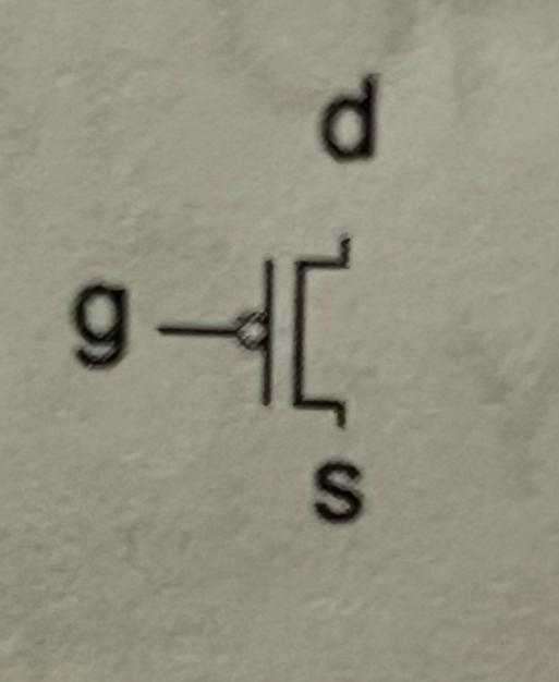
Symbol of pMOS transistor
Symbol of nMOS transistor
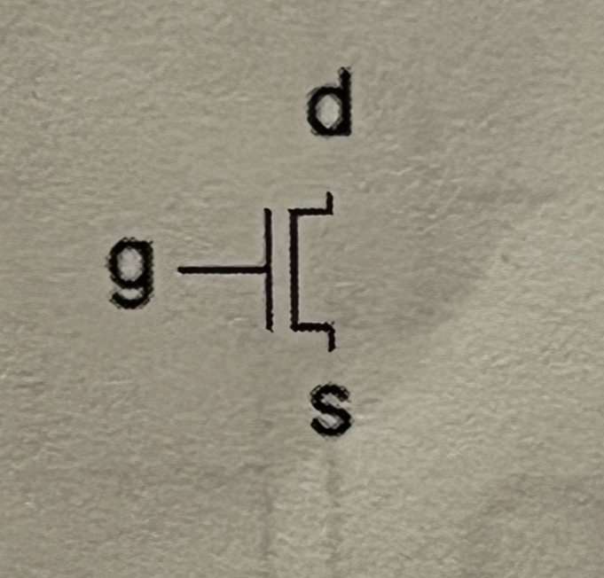
g = 0 indicates off and g = 1 indicates on
Functionality of an NMOS transistor
g = 0 indicates on and g = 1 indicates off
Functionality of a PMOS transistor
2N series
Series that are labelled as the part numbers for the discrete NMOS transistors.
BS series
Series that are labelled as the part numbers for the discrete PMOS transistors.
Layout lab
A design environment, where ICs are drawn at the mask level for fabrications
Green/Light Green
Color given for the NMOS or (n-diffusion) in an IC layout lab
Yellow/Pink inside an n-well
Color given for the PMOS or (p-diffusion) in an IC layout lab
Substrate
A base layer or surface that supports another material
Metal
Thin deposited layers of Aluminium or copper used to create interconnects (wires) between transistors and circuit blocks.
Crystalline material
A solid where atoms are arranged in a continuous, repeating 3D lattice structure (long-range order)
Polycrystalline material
A solid made of many small crystalline grains, each with its own orientation, separated by grain boundaries.
Wells
Doped regions (n-well or p-well) in the silicon substrate used to house transistors of the opposite types (PMOS in n-well, NMOS in p-well)
Polysilicon
A thin layer of polycrystalline silicon, usually heavily doped, used to form the gate terminal of MOS transistor.
Oxidation
A thin layer of silicon dioxide is thermally grown on the silicon wafer surface, used as the gate oxide of protective layer.
Polymer
Large molecules made up of repeating structural units called monomers and they play crucial roles in both natural and synthetic materials.
Photoresists
Specialized polymers that change their chemical structure when exposed to light, usually UV radiations.
Positive photoresist
A light sensitive photoresist
Etching
Removal process of selected regions of oxide or other layers (using wet chemicals or plasma) based on the photoresist pattern, to open windows for doping or deposition
Photolithography
A process where a positive photoresist is coated on the wafer then exposed to UV light through a mask to define patterns.
Doping/Ion implantation
Introducing controlled amount of n-type (P or As) or p-type (B) dopants into exposed regions of silicon to form source/drain or wells.
Polysilicon deposition
The process after ion/doping impantation.
2
No. of transistors inside an inverter
NAND and NOR
2 Logic gates are composed of total 4 transistors
6 (NAND + Inverter)
Composition of an AND gate
6 (NOR + Inverter)
Composition of an OR gate
Pull-Up-Network (PUN)
Network where pMOS transistors are present. And are always written in an SOP form.
Pull-Down-Network (PDN)
Network where nMOS transistors are present. And are always written in an POS form.
serial transistors, PUN
If parallel transistors are PUN then ________ are PDN. If parallel transistors are PDN then serial transistors are ____