Multiple Choice Questions in EAC 4: Vacuum and Semiconductor Theory
1/39
There's no tags or description
Looks like no tags are added yet.
Name | Mastery | Learn | Test | Matching | Spaced | Call with Kai |
|---|
No analytics yet
Send a link to your students to track their progress
40 Terms
Q: How many electrons are there in the fourth orbit of a copper atom?
Choices:
A. 1
B. 3
C. 2
D. 4
A. 1
Q: The maximum permissible number of electrons in the third orbit is ________.
Choices:
A. 8
B. 16
C. 18
D. 32
A: C. 18
Q: Valence orbit is the other term for ______.
Choices:
A. Outer orbit
B. 3rd orbit
C. 4th orbit
D. 2nd orbit
A. Outer orbit
Q: K shell means _________.
Choices:
A. 1st orbit
B. 2nd orbit
C. 3rd orbit
D. 4th orbit
A. 1st orbit
Q: The electrons in the largest orbit travel _________ than those in smaller orbits.
Choices:
A. More slowly
B. Faster
C. A bit slower
D. Very fast
A. More slowly
Q: What orbit controls the electrical properties of the atom?
Choices:
A. Valence orbit
B. First orbit
C. Fourth orbit
D. M shell
A. Valence orbit
What substance contains atoms with several bands of electrons but with only one valence electron?
Choices:
A. Insulator
B. Conductor
C. Semiconductor
D. Dielectric
B. Conductor
Q: Pure silicon crystal atoms contain how many valence electrons as a result of covalent bonding?
Choices:
A. 1
B. 4
C. 8
D. 16
C. 8
Q: Each atom in a silicon crystal has how many electrons in its valence orbit?
Choices:
A. 8
B. 2
C. 32
D. 4
D. 4
Q: Lifetime is the amount of time between the creation and disappearance of a/an:
Choices:
A. Free electron
B. Proton
C. Neutron
D. Ion
A. Free electron
Q: Which is a donor atom?
Choices:
A. Trivalent
B. Boron
C. Aluminum
D. Pentavalent
D. Pentavalent
Q: Silicon that has been doped with a pentavalent impurity is called a/an:
Choices:
A. N-type semiconductor
B. P-type semiconductor
C. Intrinsic semiconductor
D. Extrinsic semiconductor
N-type semiconductor
Q: In an n-type semiconductor, free electrons are called __________.
Choices:
A. Minority carriers
B. Valence electrons
C. Majority carriers
D. Charge carriers
C. Majority carriers
Q: What is the barrier potential of germanium at 25°C?
Choices:
A. 0.7V
B. 0.5V
C. 0.3V
D. 1.3V
C. 0.3V
Q: An extrinsic semiconductor is a ___________.
Choices:
A. Doped semiconductor
B. Pure semiconductor
C. Good insulator
D. Superconductor
A. Doped semiconductor
Q: Each pair of positive and negative ions at the junction is called a/an ____________.
Choices:
A. Anion
B. Positron
C. Cation
D. Dipole
D. Dipole
Q: In a pn-junction diode under reverse bias, the electric field is maximum at:
Choices:
A. Edge of depletion region on the n-side
B. Edge of depletion region on the p-side
C. Center of the n-type region
D. The PN-junction
D. The PN-junction
Q: Under low-level injection, injected minority carrier current is essentially the:
Choices:
A. Diffusion current
B. Induced current
C. Drift current
D. Recombination current
A. Diffusion current
Q: The band gap of silicon at room temperature:
Choices:
A. 1.3 eV
B. 0.7 eV
C. 1.1 eV
D. 1.4 eV
C. 1.1 eV
Q: What causes the depletion region?
Choices:
A. Doping
B. Diffusion
C. Barrier potential
D. Recombination
B. Diffusion
Q: Another name for vacuum tube diode:
Choices:
A. Thyratron
B. Fleming valve
C. Audion
D. Detector
B. Fleming valve
Q: Which terminal of the tetrode is nearest to its anode?
Choices:
A. Screen grid
B. Supressor grid
C. Cathode
D. Control grid
A. Screen grid
Q: It is the maximum permissible reverse voltage for the diode:
Choices:
A. PIV
B. Maximum voltage
C. Barrier voltage
D. Tolerable voltage
A. PIV
Q: What is another name for clamper?
Choices:
A. Slicer
B. Limiter
C. Clipper
D. DC restorer
D. DC restorer
Q: The process of converting AC to pulsating DC signal?
Choices:
A. Recombination
B. Rectification
C. Charging
D. Filtering
B. Rectification
Q: A full wave rectifier using a full input cycle has ripple frequency equal to:
Choices:
A. 60 Hz
B. 120 Hz
C. 110 Hz
D. 220 Hz
B. 120 Hz
Q: Maximum efficiency of a full wave rectifier:
Choices:
A. 50%
B. 81.2%
C. 40.6%
D. 100%
B. 81.2%
Q: Remaining variation in the output of a power supply filter:
Choices:
A. Residual voltage
B. Ripple
C. Offset voltage
D. Induced voltage
B. Ripple
Q: Type of bias required for LED to produce light:
Choices:
A. Reversed
B. Fixed
C. Forward
D. Zero
C. Forward
Q: A 50V supply drops to 45V with load. Voltage regulation is:
Choices:
A. 5%
B. 50%
C. 60%
D. 11.11%
D. 11.11%
Q: Peak output 100V. PIV for each diode in full wave center-tapped rectifier:
Choices:
A. 100V
B. 200V
C. 141V
D. 50V
B. 200V
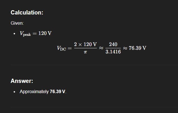
Q: DC voltage from full wave rectifier with 120V peak:
Choices:
A. 60V
B. 7.64V
C. 76.39V
D. 6.0V
C. 76.39V
Q: Band gap energy for light with 1240 nm wavelength:
Choices:
A. 1 eV
B. 2 eV
C. 1.3 eV
D. 5 eV
A. 1 eV
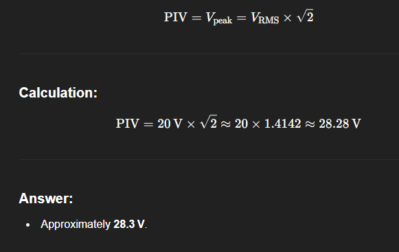
Q: RMS output 20V in bridge rectifier. PIV across diodes is:
Choices:
A. 20 V
B. 40 V
C. 28.3 V
D. 56.6 V
C. 28.3 V
Q: Ripple: 100 mV p-p, DC value: 20V. Ripple factor is:
Choices:
A. 0.05
B. 0.005
C. 0.00005
D. 0.02
B. 0.005
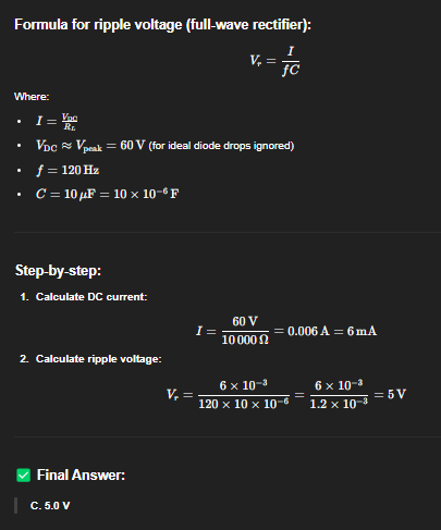
Q: 60V peak full wave rectified, f=120Hz, RL=10kΩ, C=10µF. Ripple voltage is:
Choices:
A. 0.6 V
B. 6 mV
C. 5.0 V
D. 2.88 V
C. 5.0 V
Q: Avg. input value of 200V peak half-wave rectified voltage:
Choices:
A. 63.7 V
B. 127.2 V
C. 141 V
D. 0 V
A. 63.7 V
Q: Avg. value of 75V peak full wave rectified voltage:
Choices:
A. 53 V
B. 47.8 V
C. 37.5 V
D. 23.9 V
B. 47.8 V
Q: 10Vp-p sinusoidal voltage across silicon diode and resistor. Max diode voltage:
Choices:
A. 9.3 V
B. 0.7 V
C. 5 V
D. 4.3 V
B. 0.7 V
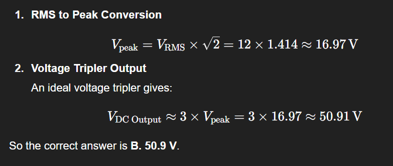
Q: Input to voltage tripler is 12V RMS. Approx. DC output:
Choices:
A. 36 V
B. 50.9 V
C. 33.9 V
D. 32.4 V
B. 50.9 V