Transistor and Amplifiers Review Questions
1/187
There's no tags or description
Looks like no tags are added yet.
Name | Mastery | Learn | Test | Matching | Spaced |
|---|
No study sessions yet.
188 Terms
1. A PNP transistor is made of
a. silicon
b. germanium
c. carbon
d. either silicon or germanium
d. either silicon or germanium
2. The transistor is usually encapsulated
a. graphite powder
b. enamel paint
c. epoxy raisin
d. black plastic
c. epoxy raisin
3. Power transistors are invariably provided with
a. solder connections
b. heat sink
c. metallic casing
d. screw bolt
b. heat sink
4. The transistor specification number 2N refers to a
a. diode
b. junction transistor
c. FET with one gate
d. SCR
b. junction transistor
5. Which of the following is necessary for a transistor action
a. the base region must be very wide
b. the base region must be very narrow
c. the base region must be made from insulating materials
d. the collector region must be heavily doped
b. the base region must be very narrow
6. As compared to a CB amplifier, a CE amplifier has
a. low current amplification
b. higher current amplification
c. lower input resistance
d. higher input resistance
c. lower input resistance
7. It is the most stable type of circuit biasing
a. self-bias
b. signal bias
c. voltage-divider bias
d. fixed bias
c. voltage-divider bias
8. The quiescent state of a transistor implies
a. zero bias
b. no output
c. no distortion
d. no input signal
d. no input signal
9. Each of the two cascaded stages has a voltage gain of 30. What is the overall gain?
a. 3
b. 9
c. 30
d. 900
d. 900
Solution: GTOTAL = (30) (30) = 900
10. Which class of amplifiers operates with the least distortion?
a. Class A
b. Class B
c. Class C
d. Class D
a. Class A
11. Which of the following circuit is the fastest switching device?
a. JFET
b. BJT
c. MOSFET
d. Triode
c. MOSFET
12. Which of the following device is unipolar?
a. FET
b. BJT
c. Zener diode
d. LED
a. FET
13. The cascaded amplifier which is often used in the IC is
a. inductively coupled
b. capacitively coupled
c. direct coupled
d. transformer coupled
c. direct coupled
14. Highest operating frequency can be expected in case of
a. bipolar transistor
b. JFET
c. MOSFET
d. IGFET
a. bipolar transistor
15. Which of the following is expected to have the highest input impedance?
a. MOSFET
b. JFET amplifier
c. CE bipolar transistor
d. CC bipolar transistor
a. MOSFET
16. The ______ is quite popular in digital circuits especially in CMOS which require very low power consumption.
a. JFET
b. BJT
c. D-type MOSFET
d. E-type MOSFET
d. E-type MOSFET
17. What is the amplification factor in FET transistor amplifiers?
a. Zi
b. gm
c. ID
d. IG
b. gm
18. The E-MOSFET is quite popular in what type of applications.
a. digital circuitry
b. high frequency
c. buffering
d. a, b and c
d. a, b and c
19. A JFET just operates with specifically
a. the drain connected to ground
b. gate to source PN junction forward biased
c. gate connected to the source
d. gate to source PN junction reverse biased
d. gate to source PN junction reverse biased
20. The main difference of a MOSFET from a JFET is that
a. JFET has PN junction
b. of the power rating
c. MOSFETs has two gates
d. MOSFETs do not have physical channel
a. JFET has PN junction
21. A small signal amplifier
a. uses only a small portion of its load line
b. always has an output signal in the mV range
c. goes into saturation once on each input channel
d. is always a common emitter amplifier
a. uses only a small portion of its load line
22. The parameter HFE corresponds to
a. β_DC
b. β_AC
c. r’e
d. r’c
b. β_AC
23. If the DC emitter current in a certain transistor amplifier is 3 mA, the approximate value of r’eis
a. 3 KΩ
b. 3 Ω
c. 8.33 Ω
d. .33 KΩ
c. 8.33 Ω

24. The input resistance of a common base amplifier is
a. very low
b. very high
c. the same as CE
d. The same as CC
a. very low
25. Each stage of a four stage amplifier has a voltage gain of 15. The overall voltage gain is
a. 60
b. 15
c. 50625
d. 3078
c. 50625
Solution: VOVERALL = (15) (15) (15) (15) = 50625
26. The maximum efficiency of a transformer coupled Class A amplifier
a. 25
b. 50
c. 78.5
d. 100
b. 50
27. In a MOSFET, the process of creating a channel by the addition of a charge carrier is called
a. inducement
b. improvement
c. balancing
d. enhancement
d. enhancement
28. What is the current gain of a common base circuit called?
a. gamma
b. delta
c. bravo
d. alpha
d. alpha
29. The name of the very first transistor
a. diode
b. junction transistor
c. point contact transistor
d. triode
c. point contact transistor
30. Region in a transistor that is heavily doped
a. collector
b. emitter
c. base
d. gate
b. emitter
31. In a common base amplifier the voltage gain is ______ (April, 2003)
a. medium
b. low
c. zero
d. high
d. high
32. In a common collector amplifier, the input resistance is ______ (Nov, 2003)
a. high
b. zero
c. medium
d. low
a. high
33. A depletion MOSFET (D-MOSFET) can operate with which of the following gate-source voltage? (Nov, 2003)
1. zero
2. positive
3. negative
a. 1 only
b. 2 only
c. 3 only
d. 1, 2 and 3
pero dida han nag answer kami c. 3 only nakadto ppt
correct: d. 1, 2 and 3
34. What problem is caused by a loosely coupled transformer in an RF amplifier? (April, 2004)
a. a too-narrow bandpass
b. over coupling
c. optimum coupling
d. a too-wide bandpass
d. a too-wide bandpass
35. Normally, how are high power tubes tested? (April, 2004)
a. visually
b. individually
c. in their circuit
d. use portable testers
c. in their circuit
1. Which are the three terminals of a bipolar transistor?
a. Cathode, plate and grid
b. Base, collector and emitter
c. Input, output and ground
d. Gate, source and sink
b. Base, collector and emitter
2. A transistor in which n-type and ptype materials are used is called
a. Unijunction
b. TTL
c. Bipolar
d. FET
c. Bipolar
3. The region in an electronic transistor that is lightly doped and very thin is referred to the
a. Collector-base
b. Collector
c. Base
d. Emitter
c. Base
4. In the BJT schematic symbol, the arrow
a. Points from p-type to n-type
b. Points from north to south
c. Points from n-type to p-type
d. Points from south to north
a. Points from p-type to n-type
5. _____ is the region in the transistor that is heavily doped
a. Collector
b. Ground
c. Base
d. Emitter
d. Emitter
6. The arrow in the symbol of a transistor indicates the direction of
a. Electron current in the collector
b. Donor ion current
c. Electron current in the emitter
d. Hole current in the emitter
d. Hole current in the emitter
7. The base of a transistor serves a purpose to what element of the FET?
a. Source
b. Ground
c. Substrate
d. Gate
d. Gate
8. ____ is the term used to express the ratio of change in the DC collector current to a change in base current in a bipolar transistor
a. Gamma
b. Beta
c. Alpha
d. Delta
b. Beta
9. Solve the collector current if the base current is 200mA and the current gain is 20
a. 10 A
b. 4 A
c. 1 A
d. 40 A
b. 4 A
10. In semiconductor technology, the characteristic of a transistor in cutoff refers to a condition when
a. The transistor is at its operating point
b. No current flows from emitter to collector
c. There is no base current
d. Maximum current flows from emitter to collector
b. No current flows from emitter to collector
11. The term “fully saturated” for a transistor refers to
a. The collector current at its maximum value
b. The collector current at its minimum value
c. The transistor beta at its maximum value
d. The transistor alpha at its maximum value
a. The collector current at its maximum value
12. The flow of electrons in an NPN transistor when used in electronic circuits is from
a. Collector to emitter
b. Collector to base
c. Emitter to collector
d. Base to emitter
c. Emitter to collector
13. A transistor acts as _____ when saturated
a. Open circuit
b. Very low resistance
c. Very high resistance
d. Variable resistance
b. Very low resistance
14. For a BJT, the BE junction is reverse biased and BC forward biased. The BJT is in what operating mode?
a. Forward active
b. Cut-off
c. Reverse active
d. Saturation
c. Reverse active
15. At this operating mode, further increase in base current will not increase the collector current.
a. Cut-off
b. Reverse active
c. Forward active
d. Saturation
d. Saturation
16. Line representing all the DC operating points of the BJT.
a. DC loadline
b. Collector curve
c. AC loadline
d. Operating line
a. DC loadline
17. In order to have the best efficiency and stability, where on the loadline should a solid state power amplifier be operated?
a. Just below the saturation point
b. At 1.414 times the saturation point
c. Just above the saturation point
d. At the saturation point
a. Just below the saturation point
18. What is another name for base bias?
a. Fixed bias
b. Gate bias
c. Emitter bias
d. Beta bias
a. Fixed bias
19. What is the most stable type of biasing
a. Current feedback
b. Fixed bias
c. Voltage divider
d. Voltage feedback
c. Voltage divider
20. Another name for voltage amplifier
a. Pre-amp
b. CE
c. Power amp
d. CB
a. Pre-amp
21. Semiconductor which is considered to be “low power” of “small signal” usually have power dissipation ratings of
a. 1 watt or less
b. 5 watts or less
c. Exactly 1 watt
d. 10 watts or less
a. 1 watt or less
22. A big metallic object that helps to cool transistors and usually attached to the collector
a. Leads
b. Bleeder resistor
c. Heat sink
d. Transformer
c. Heat sink
23. The h-parameter hf is a
a. Resistance
b. Reverse voltage gain
c. Conductance
d. Forward current gain
d. Forward current gain
24. Among the common emitter hparameters, which is the smallest?
a. hie
b. hre
c. hfe
d. hoe
b. hre
25. What is the approximate value of thermal voltage at room temperature?
a. 1 V
b. 26 mV
c. 0 V
d. 18.97 mV
b. 26 mV
26. Which of the BJT amplifier configuration has the highest power gain?
a. CE
b. CC
c. CB
d. Emitter follower
a. CE
27. Another name for common collector
a. Collector follower
b. Base follower
c. Emitter follower
d. Collector divider
c. Emitter follower
28. Which of the BJT amplifier configuration can be used as a buffer?
a. CB
b. CS
c. CC
d. CE
c. CC
29. Which transistor configuration has the highest input resistance?
a. Common base
b. Common emitter
c. Common collector
d. Common transistor
c. Common collector
30. Capacitor used to established an ac ground at a specific point in a circuit
a. Electrolytic
b. Coupling
c. Bypass
d. Choke
c. Bypass
31. What do you call an amplifier which has an output current flowing during the whole input current cycle?
a. Class AB amplifier
b. Class B amplifier
c. Class A amplifier
d. Class C amplifier
c. Class A amplifier
32. An amplifier class in which the transistor is biased way below cutoff and usually employs a tuned circuit
a. A
b. B
c. AB
d. C
d. C
33. An amplifier class in which a transistor is conducting for half of the input cycle
a. A
b. B
c. AB
d. C
b. B
34. Which statement is wrong regarding a class C amplifier?
a. Conductor angle less than 180o
b. Minimal noise
c. Biased way below cut-off
d. ηMAX = 100%
B. Minimal noise
35. Distortion at the upper end of the loadline
a. Cut-off clipping
b. Upper end noise
c. Saturation clipping
d. Compliance clipping
c. Saturation clipping
36. An amplifier with an input resistance of 600 Ωhas an input current of 500 μA. It delivers 100 mA to a 1000 Ωload. Calculate the dB gain of the amplifier.
a. 48.2 dB
b. 25.2 dB
c. 35.33 dB
d. 50.4 dB
a. 48.2 dB
37. If three amplifiers with a gain of 8 each are in cascade, how much is the overall gain?
a. 72
b. 24
c. 512
d. 8
c. 512
38. The decibel gain in cascaded amplifiers equal to the
a. Sum of voltage and current gains
b. Product of individual gains
c. Difference of individual gains
d. Sum of individual gains
d. Sum of individual gains
39. Which of the following is a characteristic of a cascaded amplifier
a. Double each amplifiers gain
b. Each amplifiers gain is increased
c. Increased overall gain
d. Total gain is decreased
c. Increased overall gain
40. ____ is a unipolar semiconductor device which the current is carried by the majority carriers only
a. Field-effect transistor
b. Point-contact transistor
c. Zener diode
d. Junction transistor
a. Field-effect transistor
41. Portion of an FET which serves as the path for current
a. Drain
b. Gate
c. Source
d. Channel
d. Channel
42. An FET can act as an excellent buffer amplifier because
a. It has a low input impedance and a high output impedance
b. It has a high input impedance and a low output impedance
c. It has a very high voltage gain and a low noise level
d. Smaller size, longer life and lower efficiency
b. It has a high input impedance and a low output impedance
43. What FET terminal corresponds to Base of BJT?
a. Drain
b. Source
c. Gate
d. Anode
c. Gate
44. The maximum value of IDfor JFET
a. 10 mA
b. IMAX
c. 100 A
d. IDSS
d. IDSS
45. Minimum VDS at which ID becomes constant when VGS is zero
a. Cut-off
b. Saturation
c. Pinch-off
d. Turn-on voltage
c. Pinch-off
46. A mode of operation for depletion type MOSFET to increase the size of the channel
a. On mode
b. Depletion mode
c. Positive mode
d. Enhancement mode
d. Enhancement mode
1. The two types of bipolar transistor are:
a. PN and NP
b. PNP and NPN
c. PPN and NNP
d. N and P
b. PNP and NPN
2. The three terminals of a bipolar junction transistor are called
a. p, n, p
b. n, p, n
c. Input, output and ground
d. Base, emitter and collector
d. Base, emitter and collector
3. The largest region of a bipolar transistor is the
a. Base
b. Emitter
c. Collector
d. N-region
c. Collector
4. The emitter of the transistor is generally doped the heaviest because it
a. Has to dissipate maximum power
b. Has to supply the charge carriers
c. Is the first region of the transistor
d. Must posses low resistance
b. Has to supply the charge carriers
5. In a PNP transistor, the p-regions are
a. Base and emitter
b. Base and collector
c. Emitter and collector
d. None of these
c. Emitter and collector
6. During normal operation, the highest percentage of electrons leaves a NPN transistor from which region?
a. Base
b. Emitter
c. Collector
d. N-region
c. Collector
7. For operation as an amplifier, the base of an NPN transistor must be
a. Positive with respect to the emitter
b. Negative with respect to the emitter
c. Positive with respect to the collector
d. 0 V
a. Positive with respect to the emitter
8. A bipolar transistor’s majority current carriers are:
a. Electrons
b. Holes
c. Dependent upon the type of transistor
d. Always both electrons and holes
c. Dependent upon the type of transistor
9. In which region is a bipolar transistor normally operated
a. Saturation
b. Cut-off
c. Linear
d. Beta
c. Linear
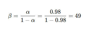
10. A transistor has a common base forward circuit gain hFE=0.98 the DC forward current gain hFEis
a. 49
b. 50
c. 98
d. Not determinable from the data given
a. 49
11. A CC amplifier has the highest
a. Voltage gain
b. Current gain
c. Power gain
d. Output impedance
b. Current gain
12. When the transistor is fully switched on, it is to be
a. Shorted
b. Open
c. Saturated
d. Cut-off
c. Saturated
13. In which operating region should normal figures calculated
a. Saturation
b. Breakdown
c. Cut-off
d. Active
d. Active
14. Which transistor circuit arrangement produces the highest power gain?
a. Common base
b. Common collector
c. Common emitter
d. A transistor’s power gain is the same in any circuit
c. Common emitter
15. The DC loadline of a transistor circuit
a. Has a negative slope
b. Is a curved line
c. Gives graphic relation between IC and IB
d. Does not contain the Q-point
a. Has a negative slope
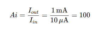
16. For an amplifying transistor, if the input signals current is 10 μA peak to peak, and the output signal current is 1 mA peak to peak and the voltage gain is 75, what is the current gain?
a. 10
b. 75
c. 100
d. 250
c. 100
17. The βDC of a transistor is its
a. Current gain
b. Voltage gain
c. Power gain
d. Internal resistance
a. Current gain
18. If in a bipolar junction transistor, Ib = 100 μA and Ic = 10 mA, what is the value of its beta?
a. 0.1
b. 10
c. 100
d. None of these
c. 100
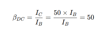
19. If Ic is 50 times larger than Ib then βDC is
a. 0.02
b. 100
c. 50
d. 500
c. 50