3B1 Amplifiers
1/40
There's no tags or description
Looks like no tags are added yet.
Name | Mastery | Learn | Test | Matching | Spaced | Call with Kai |
|---|
No analytics yet
Send a link to your students to track their progress
41 Terms
Gain of single stage amplifier (from SSM)?
How much of signal voltage is lost at each coupling?
And why?
50% when output and input impedances are matched
same impedance → voltage divider
(desirable because max power transfer and no reflections)
Steps to design bipolar transistor amplifier?
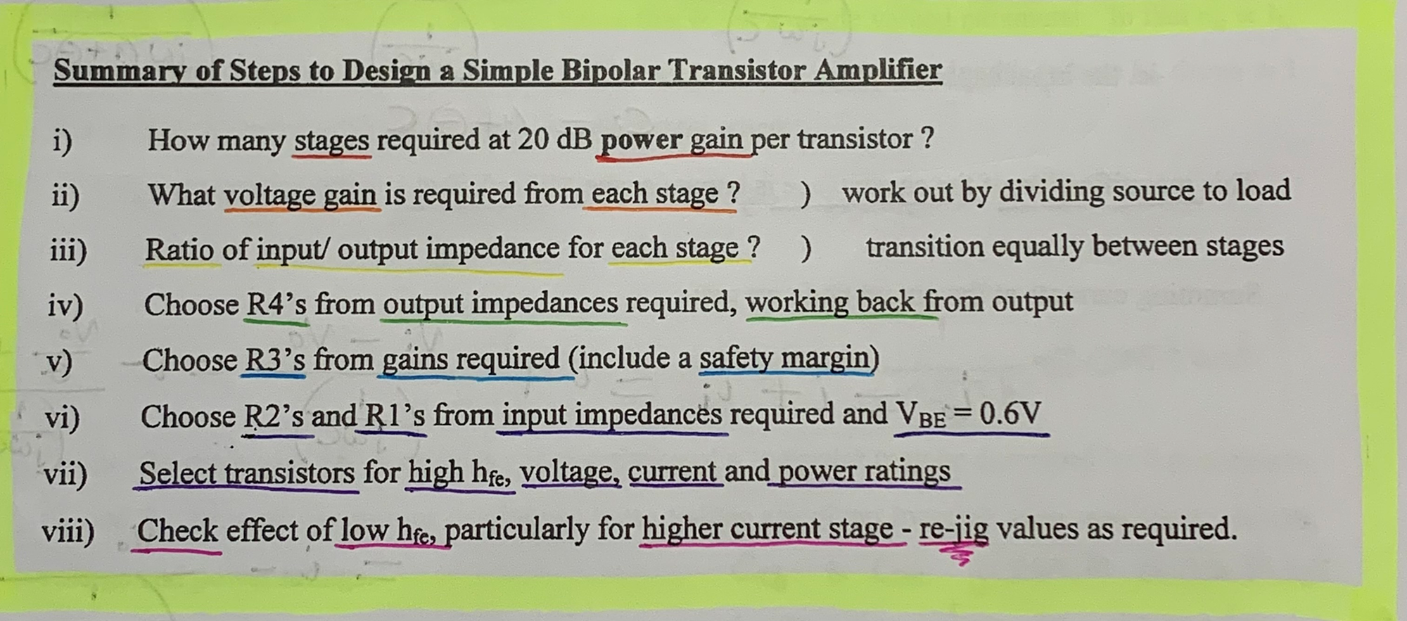
Choose series capacitors
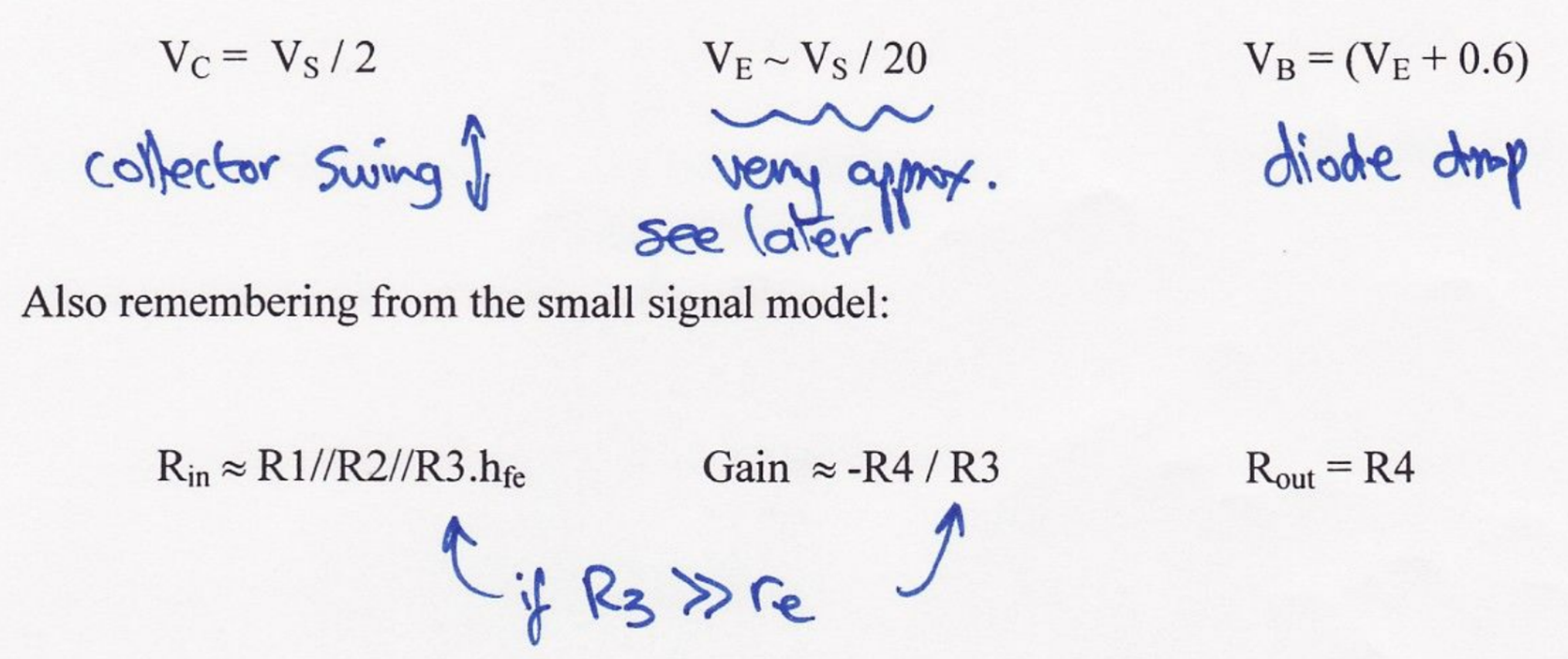
What should the output bias be and why?
Half the supply voltage ( whether emitter or collector)
Allows maximum voltage swing without clipping
Gain and output impedance for collector output?
Gain >1 & inverting
output impedance = R4
Gain and output impedance for emitter output?
Gain ≈1 & non-inverting
Output impedance = re
Convert Vpp to Vrms?
β Vrms = 2√2 β Vpp
i.e. multiply rms value by 2√2
Ebers-Moll equation?

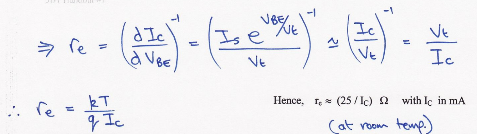
Equation for Vt?
And value at room temp?
Vt = kT/q
~25mV at room temp
Why can we ignore the base-emitter voltage and collector-emitter conductance in SSM?
base-emitter voltage: represents Early effect (voltage coupling between C & B)
collector-emitter conductance: negligible compared to collector load
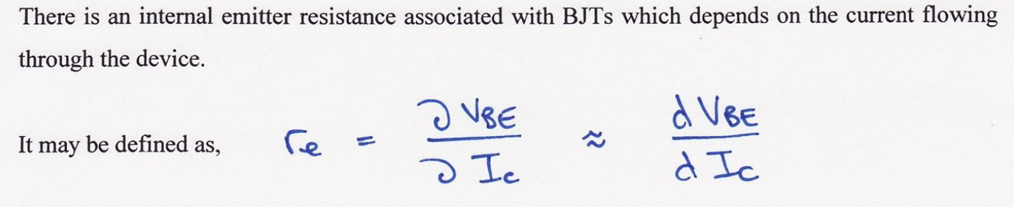
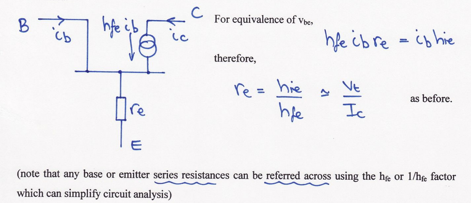
Derive emitter resistance equation?
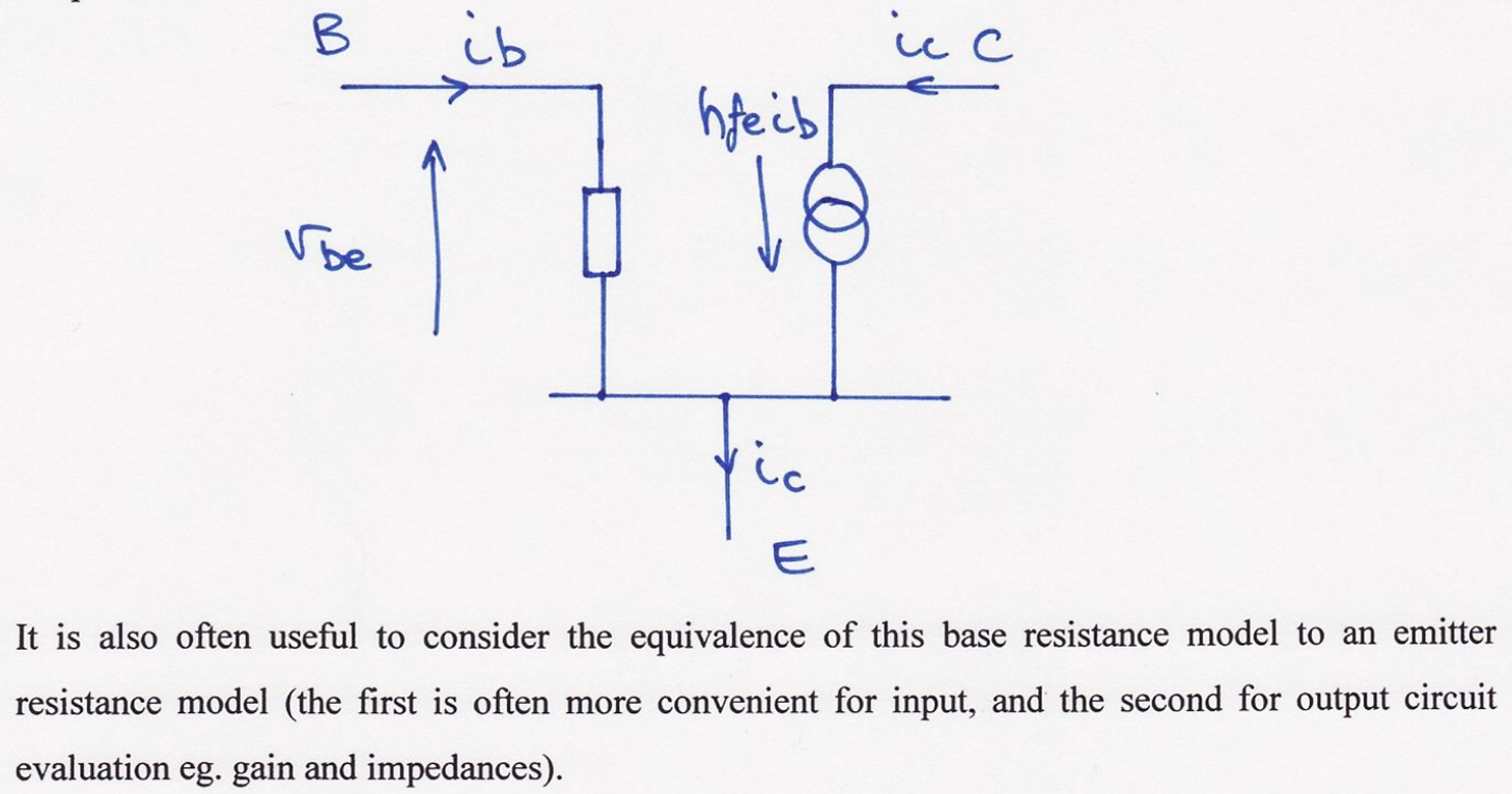
hie & hfe relationship equation derivation?
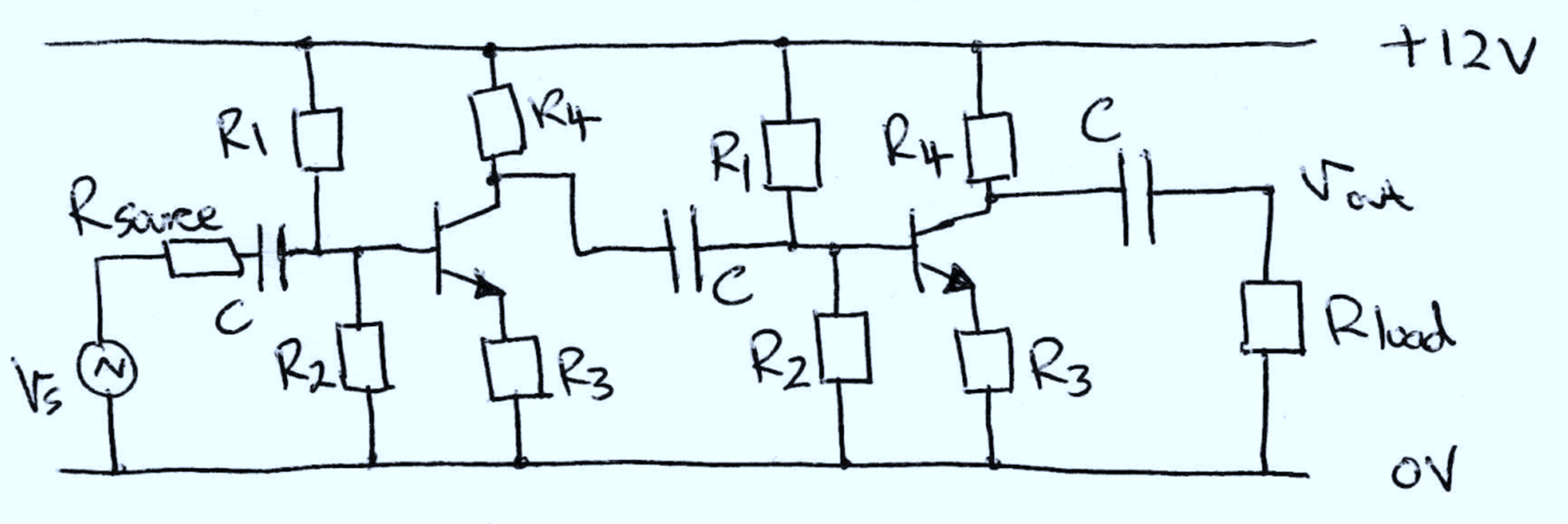
Role of passive components in transistor amplifier circuit?
C : ac signal coupling capacitor (isolates dc bias levels between stages)
R1 & R2 : form a voltage source to provide a dc base bias current
R3 : provides negative feedback to the base bias current to stabilise bias point
R4 : collector output load resistor (changes in collector current create an output voltage swing)
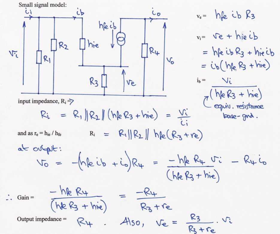
Find input impedance of this SSM?
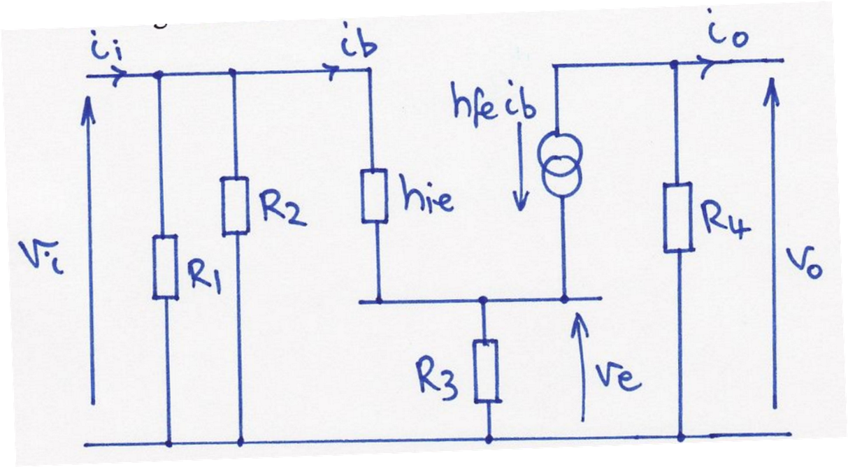
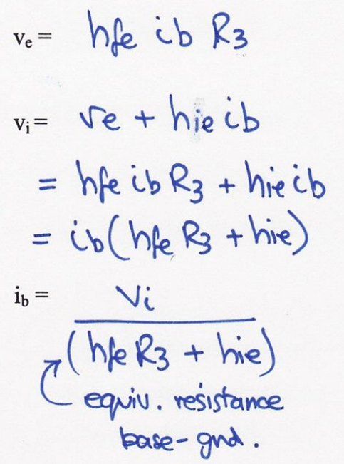
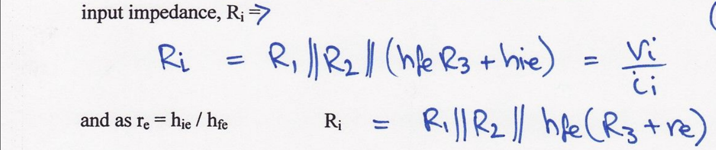
Find gain, output impedance and ve of this SSM?
What should Ebers-Moll be used for?
large signal properties
Rules to select R1-R4 for each stage?
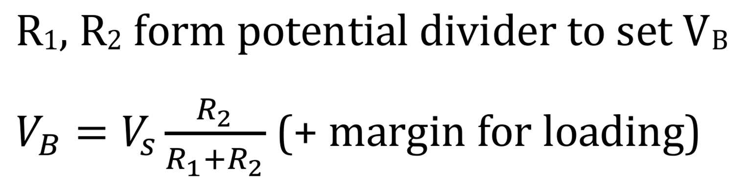
margin = + 20 % (to allow for base current loading) — 1.2 VB = Vs (R2 / R1 + R2)
R₂ ≈ 2× Rin
R₁ ≈ 2× Rin
^^(choose one at a time and see if value of other one would be permissible)
Check R₁ and R₂ in parallel give correct input impedance
Choose in order: R4, R3, R2, R1
Why is margin for base-current loading needed?
Diode between B & C, so VBE has to be above certain value to turn transistor on
What to consider in higher current devices?
hfe often lower, so check hfe = 50 as well to make sure there are no issues with input impedance and gain across stages
^^requires more base current for given collector current from bias resistors
^^must be able to provide this without appreciable voltage drop
When is matching impedance not necessarily important?
High output impedance—probably not a power circuit
What low frequency response roll-off/ frequency cut-off should you choose?
20 Hz
f-3dB and trise equations?
f-3dB = 1 / 2πRC
trise = 2.2 RC
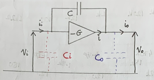
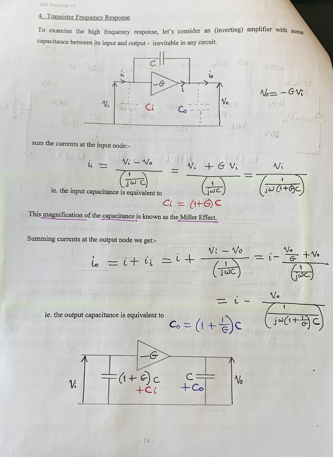
Show Miller effect for this inverting amplifier?
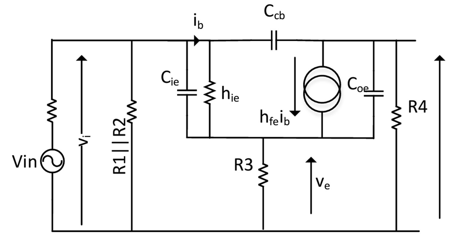
Where to draw Ccb, Cie and Coe on SSM?
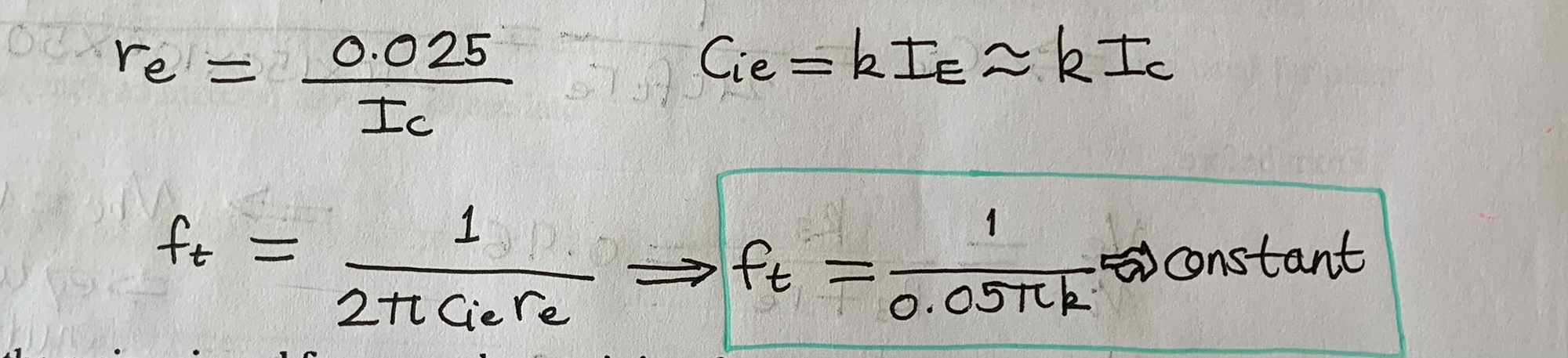
Derive ft equation?
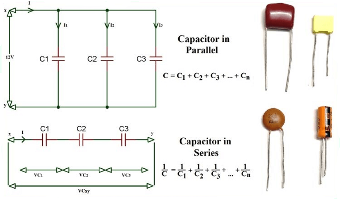
Sum capacitors in series vs parallel?

Method to find -3dB freq using internal capacitances?
Draw SSM with Ccb, Cie and Coe
Use ft equation to find Cie
Simplify SSM by referring hie, cie to ground
ve / vi = R3 / (R3 + re) = 0.96
cie, hie to ground need factor of 1/(1-0.96) = 25
plot voltage source and Rin in series
plot in parallel: R1//R2 , 25 hfe re (= hie) , cie / 25 , (1+G) ccb
f3dB = 1 / 2π R’ C’
[add output circuit equivalent too]
What can you do if Rin too high?
Reduce both R1 and R2 by same percentage
Briefly describe Miller effect?
Causes a capacitance between input and output of an inverting amplifier to appear magnified by the amplifier gain
How do you show Miller effect?
And what are the capacitance results?
[upload picture of your notes]
limits the bandwidth of RF amplifier circuits by increasing effective capacitance at input
How to mitigate Miller effect?
Want higher input impedance so CR time constant is small
Use pair of transistors:
1 provides voltage gain (with low input impedance)
1 provides input path with low capacitance (but no voltage gain)
E.g.
[upload pictures of differential amplifier & cascode circuit]
Schematic of 2-stage RF amplifier?
What do you divide to find impedance blending?
source / load
Why choose large C?
Should have small impedance to give low frequency response roll-off
How to find VE?
VE = IC R3
What is ve/vi?
Emitter gain
Where to draw source and load resistances on SSM?
Source = series
Load = parallel
Which gain should you use for SSM Miller effect?
Voltage gain
÷2 for LOADED!!
How can you compensate for -3dB freq too close to operating freq?
Decrease R3
(increases overall amplifier gain)
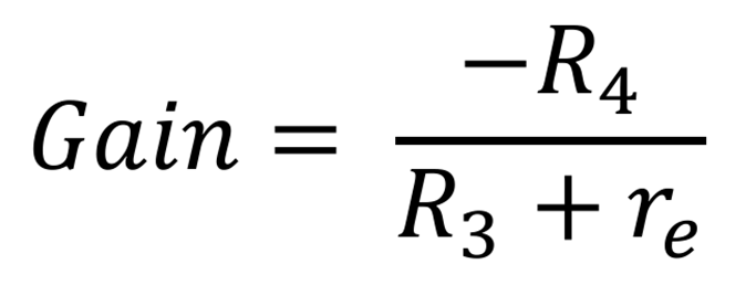
vo / vi = -R4 / (R3 + re)
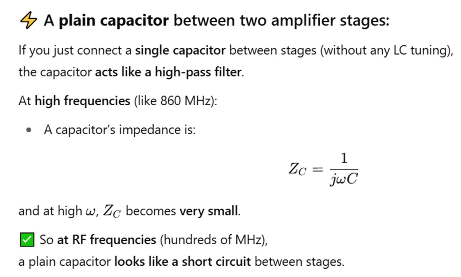
Plain capacitor between amplifier stages?
How does an LC circuit select certain frequencies?
Series LC
Resonance: acts like short circuit (impedance = 0 at 860 MHz)
Off resonance: impedance rises (signals far from 860 MHz are attenuated)