MTE3203 Week 7 Electric and magnetic properties
 Call Kai
 Learn
Learn Practice Test
 Spaced Repetition
 Match
Match Flashcards
 Knowt Play
1/15

There's no tags or description
Looks like no tags are added yet.
Name | Mastery | Learn | Test | Matching | Spaced | Call with Kai | Chat |
|---|
No analytics yet
Send a link to your students to track their progress
16 Terms
Total conductivity of a ceramic
σ_total = σ_electronic + σ_ionic. Current is carried by electrons and holes, by whole ions hopping through the lattice, or by a mixture of both.
How the bandgap classifies a material
A full band cannot conduct — every seat is taken, so an electron must reach the empty conduction band at a cost of E_g. Above 4 eV nothing crosses (insulator); 0.02–4 eV (semiconductor); metals have no gap because their single band is only half filled.
σ = neμ: what you can actually change
Only two things. n is the number of mobile carriers, μ is mobility. Raising conductivity in a ceramic means raising one or both — there is no third option.
What lowers electron mobility
Anything that breaks the periodic lattice: dislocations, point defects, grain boundaries. Electrons travel smoothly through a perfect repeating structure and scatter off irregularities, which shortens the distance travelled between collisions.
Why wide-gap ceramics never conduct thermally (MgO)
n_i = (N_cb·N_vb)^½ exp(−E_g/2kT). Reaching 10^17 carriers/cm³ in MgO requires about 9800 K, roughly three times its melting point. So any conductivity actually measured must come from defects or impurities, never from heat.
ITO: why doping matters in a wide-gap ceramic
In2O3 has a 3 eV gap and about 10^−7 carriers/cm³ — effectively an insulator. Adding 2.5% Sn gives ~10^21 carriers/cm³ and σ ≈ 10^4 S/cm. Doping does not improve the conductivity, it creates it. Transparent because a 3 eV gap does not absorb visible light.
What ionic conduction requires
An ion can only move if there is an empty site next to it: a vacancy, an unfilled interstitial, a Schottky defect or a Frenkel defect. Best in open lattices and layered structures, and steeply temperature-dependent through D = D0·exp(−Ea/kT).
Doping to create vacancies
Substituting an ion of different charge forces the crystal to create vacancies to stay neutral. Ca2+ on a Na+ site gives a cation vacancy (helps cation transport); O2− on a Cl− site gives an anion vacancy (helps anion transport). This is the basis of YSZ oxygen sensors and fuel cell electrolytes.
Superconductivity: definition and mechanism
Below the critical temperature T_c, resistivity is exactly zero and magnetic field is expelled — both, not just the first. BCS theory explains the low-temperature case through Cooper pairs formed by lattice distortion. The high-T_c ceramic pairing mechanism is unknown; it occurs in the CuO2 layers. Limits: brittle and expensive.
Dielectrics which polarise for storing more charge in capacitor
The dielectric polarises in opposition to the electric field, weakening this field between plates in a capacitor, so they accept more charge before reaching the same voltage. k′ multiplies stored charge directly.
The four polarisation mechanisms
Electronic (electron cloud sags off its nucleus)
ionic (lattice distorts and ions shift apart)
orientation (dipoles that already exist rotate into line)
space charge (charge accumulates at phase boundaries). They sum to α_total, and which ones are available is what sets k′.
Paraelectric vs ferroelectric BaTiO3
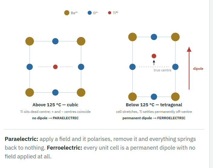
Above Curie temp it is cubic with Ti4+ centred and symmetric, so there is no built-in dipole and it polarises only while the field is applied. Below curie temp it is tetragonal with Ti4+ permanently off-centre, so every unit cell is a permanent dipole with no field applied. THis is how material switch betweeen paraelectric and ferroelectric
Why ferroelectric k′ of BaTiO3 is so large
The permanent dipoles (from offcentre Ti) organise into domains. An applied field reorients whole domains at once instead of nudging individual electron clouds, so millions of existing dipoles align together —
Piezoelectric effect and its structural requirement
One more consequence of the off-centre titanium in BaTiO3. A field pushes the ion sideways — and pushing an ion sideways also changes the cell's shape.
That two-way link between electric field and mechanical deformation is the piezoelectric effect. Mechanical strain producing an electrical signal is the direct effect, and an applied field producing strain is the reverse piezoelectric effect
Requirement:
an anisotropic crystal with no centre of symmetry
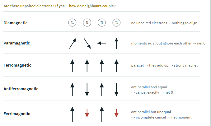
The five magnetic classes
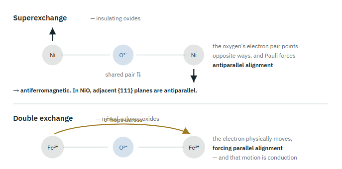
Superexchange vs double exchange