ELEX - EDC (Transistors) - A
1/40
There's no tags or description
Looks like no tags are added yet.
Name | Mastery | Learn | Test | Matching | Spaced |
|---|
No study sessions yet.
41 Terms
The current flow across the base-
emitter junction of a PNP transistor:
a. mainly electrons
b. equal numbers of holes and
electrons
c. mainly holes
d. the leakage current
C
In PNP, what can you say about its
collector current?
a. no base current
b. negative with respect to source
c. flows from emitter to collector
d. dependent on emitter
C
In a transistor, the base current is
about ___ of emitter current.
a. 25%
b. 20%
c. 35%
d. 5%
D
The primary function of the bias
circuit is to:
a. hold the circuit stable at vcc
b. hold the circuit stable at
c. ensure proper gain is achieved
d. hold the circuit stable at the
designed Q-point
D
When is degeneration tolerable in
an amplifier?
a. When it is necessary to prevent
amplitude distortion.
b. If an increase in signal amplitude
aside from the rated value is needed
c. When a decrease in signal
amplitude aside from the rated value
is needed
d. If stabilit is needed
A
The disadvantage of base bias is
that:
a. it's very complex
b. it produce low gain
c. it's too beta dependent
d. it produces high leakage current
C
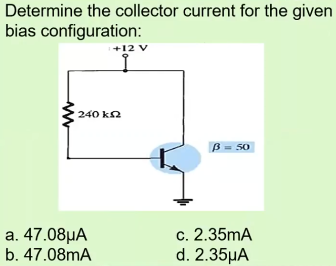
C
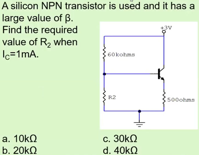
D
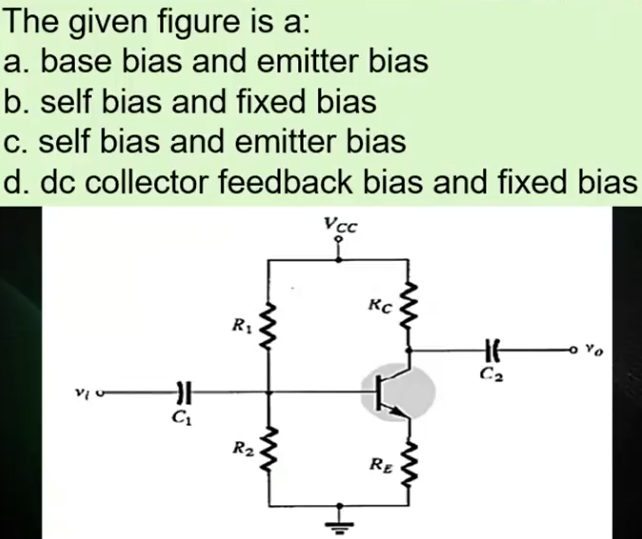
B
If a splash of solder shorts the
collector resistor of TSEB, the collector
voltage will:
a. Drop to zero
b. Equal the collector supply voltage
c. Stay the same
d. Double
B
The saturation current of a transistor
used in a fixed bias circuit is __ its
value used in an emitter-stabilized or
voltage-divider bias circuit for the same
values of Rc.
a. more than
b. the same as
c. less than
d. None of the above
A
What term is used to indicate current
gain in a common-collector configuration?
a. Alpha
b. Beta
c. Gamma
d. X-ray
C
A transistor has a current gain of 0.99
in the CB mode. Its current gain in the
CC mode is:
a. 100
b. 99
c. 1.01
d. 0.99
A
In a transistor-switching network,
the operating point switches from ___
to ___ regions along the load line.
a. cutoff, active
b. cutoff, saturation
c. active, saturation
d. None of the above
B
To amplify voltage, current and power
signals using BJT amplifiers, which of the
following configuration is used?
a. common collector, common base and
common emitter
b. common base, common emitter and
common collector
c. common emitter, common collector and
common base
d. common base, common collector and
common emitter
D
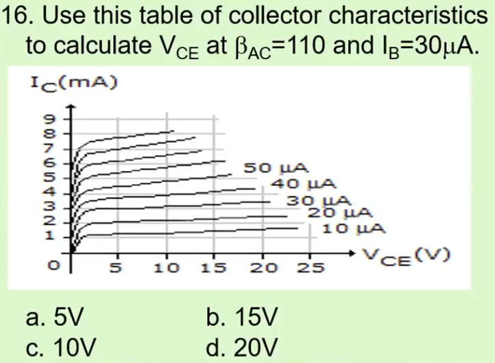
B
The phase shift in the common-collector
and common-base amplifier is:
a. 270 degrees
b. 180 degrees
c. 90 degrees
d. 0 degrees
D
A certain common-emitter amplifier
has a voltage gain of 100. If the
emitter-bypass capacitor is removed,
a. the circuit will become stable
b. the voltage gain will decrease
c. the voltage gain will increase
d. the Q-point will shift
B
The gain of the transistor in common
emitter amplifier circuit is 100 at a
frequency of 1000Hz. The gain is 70.7 at
335 KHz. The gain drops to 1 at 210MHz.
The alpha-cutoff is:
a. IKHz
b. 335KHz
c. 210MHz
d. none of the above
B
Manufacturers data sheets specify
transistors using ___ parameters.
a. r
b. h
c. s
d. z
B
Which of the following is referred to
as the reverse transfer voltage ratio?
a. hi
b. hr
c. hf
d. ho
B
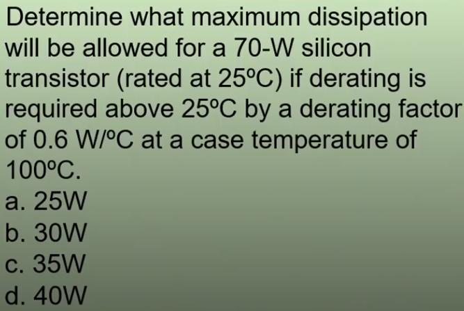
A
Maximum power dissipation in BJT
transistor occurs at:
a. base junction
b. collector junction
c. emitter junction
d. at the pn junction
B
What two primary items determine the
class of operation of an amplifier?
a. The amount of bias and the
amplitude of the input signal
b. DC and AC analysis
c. Amplitude of the input and output
signal
d. Fidelity and Efficiency
A
Class ____ eliminates crossover
distortion found in pure class B.
a. A
b. AB
c. C
d. D
B
What is the maximum collector
efficiency of a resistance loaded
class A power amplifier?
a. 50%
b. 78.50%
c. 25%
d. 30%
C
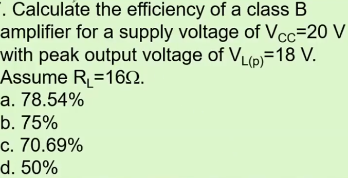
C
A Darlington transistor has:
a. A very low input impedance
b. Three transistor
c. A very high current gain
d. One VBE drop
C
What is the key to FET operation?
a. The amount of voltage that will control
the conduction
b. Effective cross-sectional area of the
channel
c. The amount of current that will control
the conduction
d. The low input impedance compared
with the high output impedance
B
In an N-channel JFET, pinch-off occurs
when the gate bias is:
a. slightly positive
b. zero
c. slightly negative
d. very negative
D
What is the "pinch off' voltage of an
FET?
a. The voltage required for the FET to
conduct
b. The voltage required to overcome the
FET reverse bias
c. The voltage required to reduce drain
current to zero
d. The voltage required to reduce gate
voltage to zero
C
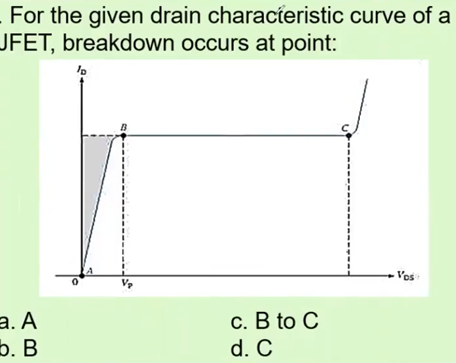
D

C
When internal temperature increases in a
power FET, the:
a. The threshold voltage increases
b. Gate current decreases
c. Drain current decreases
d. Saturation current decreases
C
For an n-channel enhancement type
MOSFET, if the source is connected at a
higher potential than that of the bulk
(VSB > 0), the threshold voltage VT of the
MOSFET will:
a. remain unchanged
b. decrease
c. change Polarity
d. increase
A
A gate to drain-connected enhancement
mode MOSFET is an example of:
a. an active load
b. a switching device
c. a three-terminal device
d. a diode
A
The threshold voltage of an n-channel
enhancement mode MOSFET is 0.5 when
the device is biased at a gate voltage of
3V. Pinch off would occur at a drain
voltage of:
a. 1.5V
b. 2.5V
c. 3.5V
d. 4.5V
B
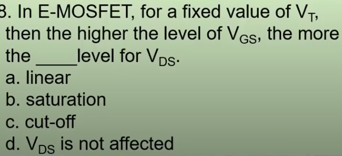
B
An n-channel E-MOSFET conducts when
it has:
a. VGS > VP
b. an n-type inversion layer
C. VDS > 0
d. depletion layers
B
An E-MOSFET that operates at cut-
off or in the ohmic region is an
example of:
a. a current source
b. an active load
c. a passive load
d. a switching device
D
When transistors are used in digital
circuits they usually operate in the:
a. active region
b. breakdown region
c. saturation and cutoff regions
d. linear region
C