04 Semiconductors
1/50
There's no tags or description
Looks like no tags are added yet.
Name | Mastery | Learn | Test | Matching | Spaced |
|---|
No study sessions yet.
51 Terms
What characterizes Semiconductors relative to its conductivity?
Conductivity between conductivity of a conductor and of an insulator
Around 1 × 10⁻² to 1 × 10² (Ωm)-1
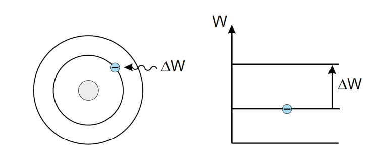
Which orbits correspond to a higher energy?
Outerer orbits
Addition of energy is needed to bring one electron from an inner orbit to an outer orbit
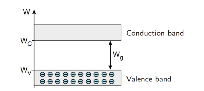
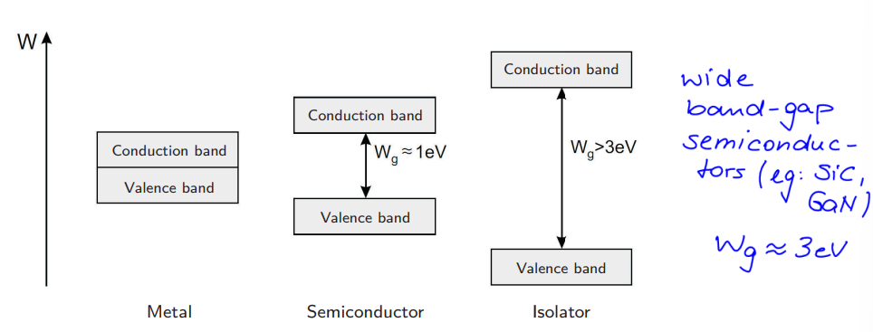
What are energy bands?
Groups of energy states in solids
The gaps between energy bands are called band gaps
We consider Valence Band - Band Gap - Conduction Band

Where are the electrons at T = 0 K?
In the valence band
The conduction band is empty
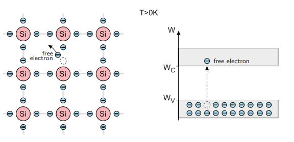
How many valence electrons has silicon?
4
What is the effect of heating up a silicon crystal?
Moving an electron form the valence band to the conduction band, allowing carge transport (a full band does not transport charges)
The higher the temperature, the more free electrons there are in the conduction band
What is the intrinsic conduction carrier density?
The density of free electrons
What is generation?
Creation of new mobile charge carriers by an electron jumping into the conduction band
What is generated is one free electron in the conduction band and one hole in the valence band
At a thermal equilibrium, the rate of generation and of recombination is the same
What is recombination?
Anhilation of mobile electron-hole pair by an electron losing energy and falling back into the valence band
At a thermal equilibrium, the rate of generation and of recombination is the same
What is the relationship between conductivity and band gap size?
The smaller the band gap, the easier for electrons to enter the conduction band → material is a good conductor
Semiconductors have a medium size band gap
(There exist wide band-gap semiconductors, tho)
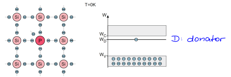
What is an n-doped semiconductor?
Intrinsic semiconductor with inclusion of pentavalent element (e.g. P)
Band gap of the fifth electron of the donator element is smaller than the band gap of the conductor
More electrons than holes
Electrons are majority charge carriers
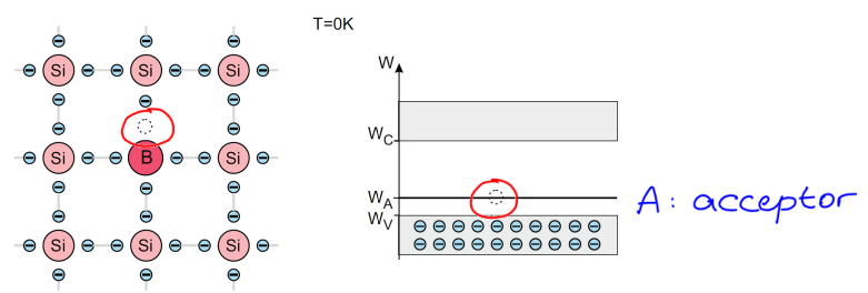
What is an p-doped semiconductor?
Intrinsic semiconductor with inclusion of trivalent element (e.g. B)
Band gap from the acceptor to the valence band is very small, so electrons can be easily absorbed by the valence band of the conductor
More holes tham electrons
Holes are majority charge carrier
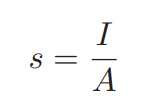
What causes a current flow?
Free movement of electrons or holes within the semiconductor
s is the current density
A is the cross-sectional area of the conductor
The total current density equals the sum of the electron and hole curren densities
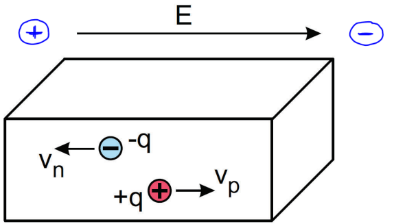
What are drift currents?
If an electric field E is applied to a semiconductor, the charge carriers experiment a force: electrons against the field and holes with the field direction
The velocity of the charge carriers is their averaged rate of displacement, since they do not accelerate arbitrarily due scattering by the crystal grid. Therefore, the velocity is constant
How is the average carrier velocity defined?
Negative for electron displacement
Positive for hole displacement
Product of respective mobility factor μ and applied Electric Field
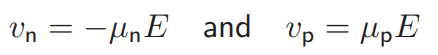
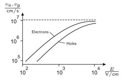
What is the general behavior of μ?
Almost constant at lower field strengths
Decreases with increasing field strength (due to scattering)
Decreases with increasing temperature
Decreases with doping intensity
How is the drift current density defined?
As the sum of the electron and hole current densities
Current density of a charge carrier is the absolute value of its speed multiplied by the respective charger density (n or p) and the elementary charge q
Mobility factor, elementary charge and charger density is summarized by the parameter σ (conductivity)

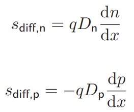
What is diffusion?
Movement of free particles of a region of higher concentration to a region of lower concentration
How are the diffusion currents defined?
As independent of the electric field and the charge of the particles
Negative for holes
Positive for electrons
As a derivative of the charger density with respect to its position in the junction
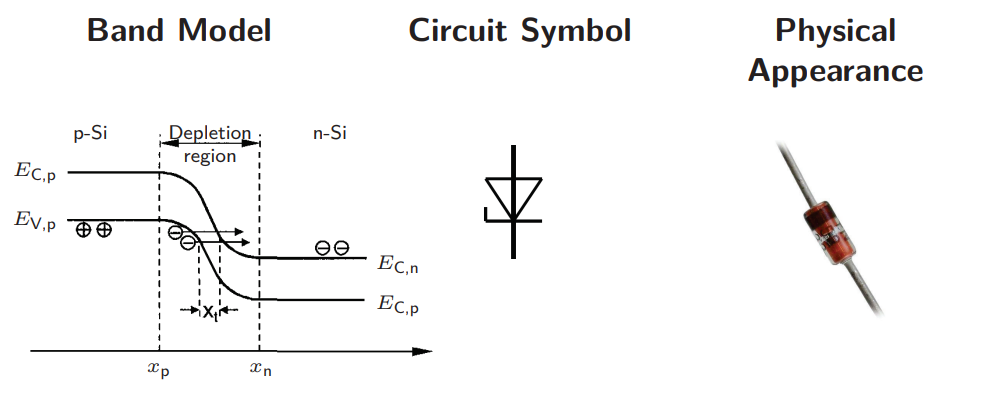
What is a p-n junction?
A p-doped region connected with an n-doped region
Implies diffusion of holes into the n-region and of electrons into the p-region
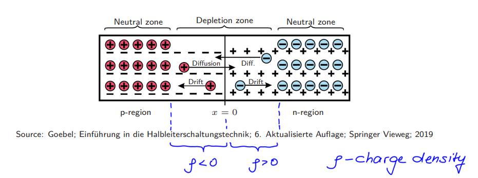
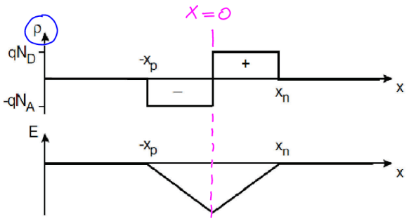
How is the depletion zone created?
By the diffusion of the charge carriers in the opposite direction, leaving a net opposite charge in their respective region (electrons leave a positive charge in the n-region and holes leave a negative charge in the p-region)
The charge difference at both sides of the depletion zone generates an eelctric field (from positive to negative)
The electric field leads to the drift of electrons and holes (electrons against the field and towards the n-region, and holes with the field and towards the p-region)
Diffusion current and drift current get into thermodynamic equilibrium

How do the charge density and the electric field behave at the p.n junction?
Electric field ressembles the integration of the charge density over the distance of the junction
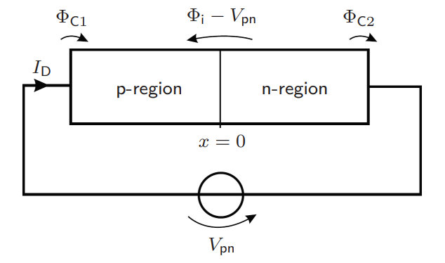
How does the semiconductor diode works?
Blocks the current until enough voltage is applied to get the pn-junction conducting
Widely considered, allows current flow in one direction and blocks current flow in the other

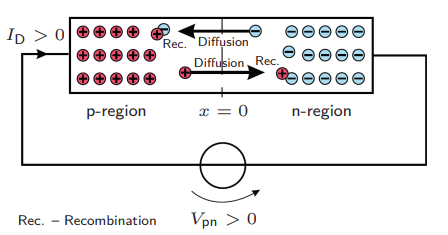
What is the behavior of the semiconductor diode for Vpn > 0?
Electric field in the junction decreased
Diffusion dominates
Depletion zone gets smallers
Electron flow in the p-region leads to recombination
Electric potential decreses (flow decreses the “will“ of charge carriers to cross the junction, since they are already crossing)
What is the behavior of the semiconductor diode for Vpn < 0?
Electric field in the junction increased
Drift dominates
Depletion zone increases in size
Generation of electron-hole pairs and flow from p-region to n-region
Blocking direction is established
Electric potential increses (blocking in the junction increases the “will“ of the charge carriers to go across)
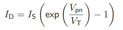
How is the current in a diode defined?
As the saturation current increased by the exponential of Vpn/VT - 1
VT the Temperature Voltage
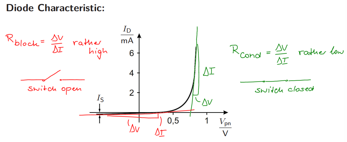
How can be the Diode Characteristic be expressed in terms of resistance?
R is very high (switch open) for blocking state (ΔV > ΔI)
R is rather low (switch closed) for conducting state (ΔV < ΔI)

What happens when the voltage (| V |) in the reverse direction is high? Recall: reverse direction means negative voltage
Current increases sharply above certain value
Breakdown
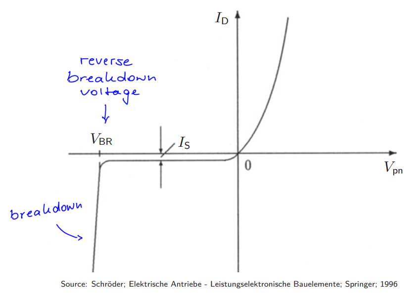
What are the different types of breakdown?
Avalanche Breakdown: generated charge carriers lead to more electron-hole pairs collisions with atoms of the grid (for higher voltages and lightly doped junctions which have therefore larger depletion zones)
Zener (Tunnel) Breakdown: high doping and smaller voltages lead to a smaller depletion region, causing the tunneling from charge carriers from the valence band into the conduction band
Thermal Breakdwon: destructive breakdown of the component if the permitted power dissipation of the diode is exceeded
What are Zenner Diodes?
Used for:
Voltage limitation
Voltage Stabilization
Operation in reverse direction
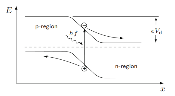
What are LEDs?
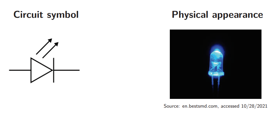
Light Emitting Diodes
Recombination for voltage in forward direction
Energy released during recombination, emitted as a photon (electroluminescence)
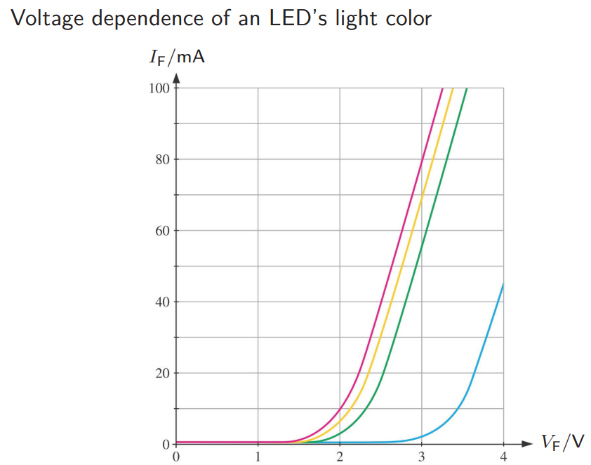
Emitted power proportional to forward current
Light wavelength depending on the band gap (the higher the band gap, the higher the required forward voltage)
The smaller the wavelength, the higher the forward voltage
The wider the band gap, the smaller the wavelength
Used for:
Lighting
Radiation of infrared light in sensor technology
Generation of UV radiation
Singal generation in optical fibers
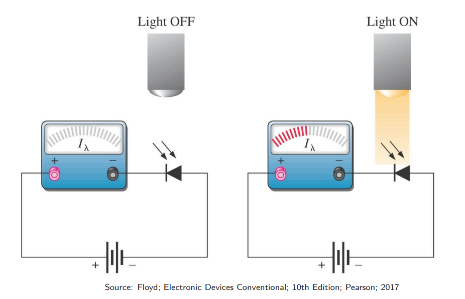
What are photodiodes?
Raised in energy of electrons in the pn-junction by light irradiation
Light energy is sufficient to overcome deplation zone
What are technical applications of diodes? (1)
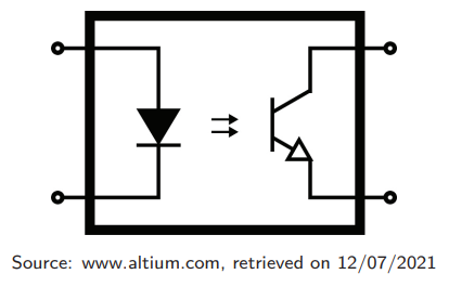
Galvanic isolation in circuits (e.g. Optocouplers): LED + Photoreceiver (Photodiode or Phototransistor) to transmit signals purely optically at extremley high cut-off frequencies
What are technical applications of diodes? (2)
High Voltage Direct Current (HVDC) transmission
Switching of line votlages without additional transformers for control circuits
What are active components?
Components that allow a circuit to output more power than the provided by its energy source (e.g. amplifier)
Transistors are active components
Active elements are modelles as switches: open/closed states (power electronics)
What are the big two types of transistors?
Bipolar Junction Transistors (BJT)
Field Effect Transistors (FET)
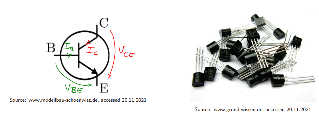
What are BJTs?
Bipolar Junction Transistor
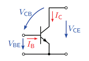
Implement 1 low power terminals (B - base) and 2 high power terminals (C - collector and E - emitter) (Diagram order: CBE)
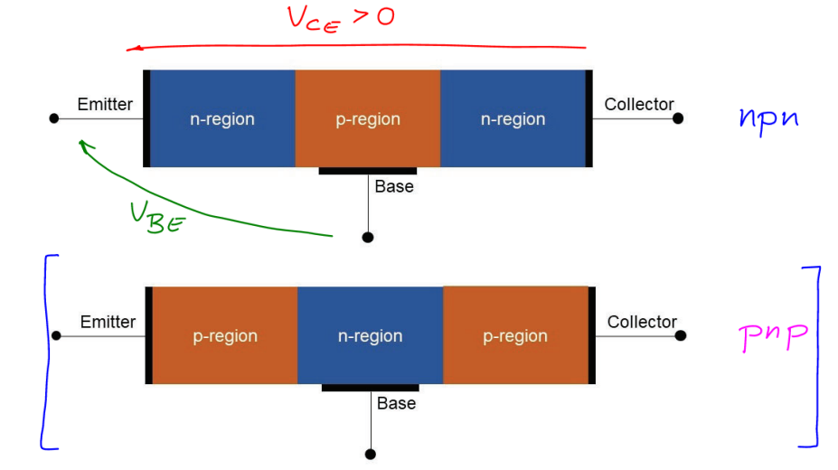
Correspond to two pn-junctions in series (either npn or pnp)
What are the operation modes of a BJT?
Output goes in the positive-to-negative direction
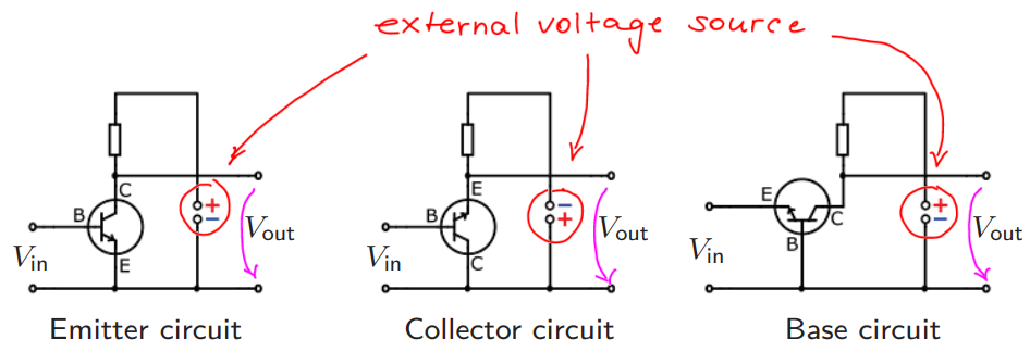
Emitter Circuit: most common and suitable for amplifier circuits (Input: B; Output: Collector)
Collector Circuit: high input resitance with low output resistance (Input: B; Output: Emitter)
Base Circuit: low input resitance with high output resistances (Input: Emitter; Output: Collector)
How does a transistor work?
Modelled using emitter circuit of an npn bipolar transistor
Positive voltage between collector and emitter VCE > 0 (due to potential) leads to reverse mode. No current flows through the collector and base IC = 0
If a positive base-emitter votlage is applied VBE > 0 (exceeding the diffusion voltage of the transistor), a current starts to flow thorugh collector and emitter, turning the transistor into conductive state
In normal operatior IB « IC
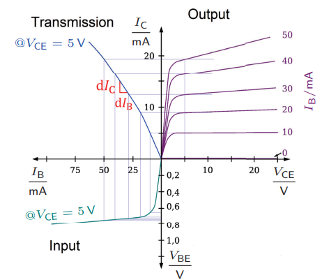
What does the current thorugh the transistor depend on?
On the base-collector voltage and the base current
There are 3 regions to be observed:
Saturation area (from A to B)
Linear/Active Range (from B to C) (never use it for power electronics)
Breakdown Area (from C onwards)
For power electronics applications: use it in the saturation are
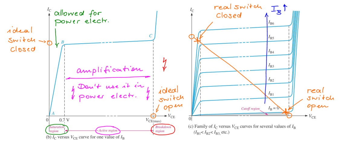
How does the characteristic of a BJT look like?
With gain factor β defined as the slope of the transmission curve
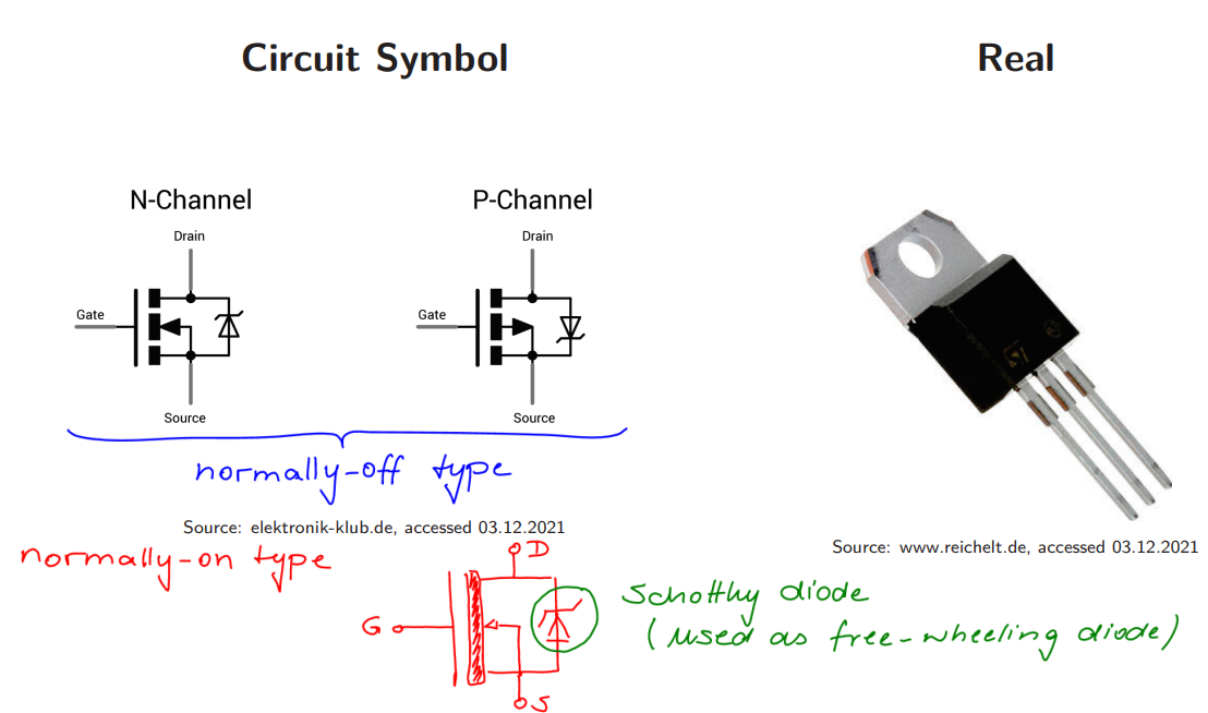
What are MOSFETs?
Metal Oxide Semiconductor Field-Effect Transistors
Have normally-off and normally-on variants
Three terminals: Gain (G), Drain (D) and Source (S)
Classified into n-channel and p-channel according to their internal structure
Have 3 operation modes:
Source Circuit (cf. Emitter Cirucit)
Drain Circuit (cf. Collector Circuit)
Gate Circuit (cf. Base Circuit)
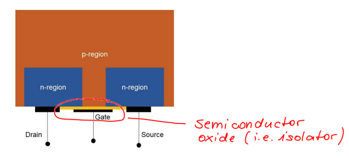
How is a MOSFET structured?
Gate connected to the doped regions via semiconductor exide (i.e. insulating layer)
Upon applying voltage, the insulated connection effects an electric field between the drain and source, allowing or preventing current flow
At low frequencies at the gate inpute, the MOSFET requires very low power
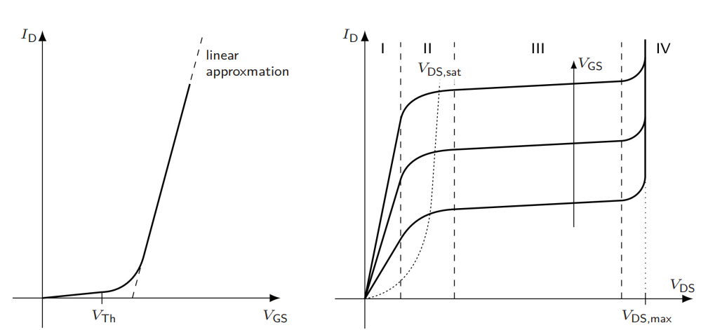
How does the characteristic of a MOSFET look like?
Three regions:
Ohmic/triode Range
Saturation Range
Breakdown Range
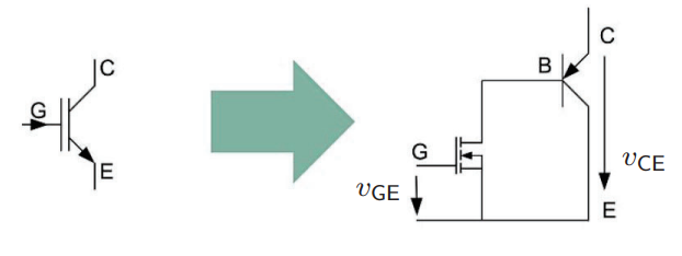
What are IGBTs?
Insulated-Gate Bipoler Transistors
Combination of advantages of BJTs (high reverse voltage with low forward restance) + MOSFETs (little power required for driving)
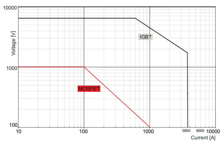
Suitable for high-power, high-voltage and high-current appplications
Terminals: Collector (C), Gate (G), Emitter (E)
How are IGBTs structured?
Darlington circuit of pnp-BJT and n-channel MOSFET used to large currents that need to be switched with low powers
Controlled through the MOSFET gate. If gate-emitter VGE exceed the threshold voltage, current flows across the BJT
How does the characteristic of an IGBT look like?
3 Regions:
Reverse Blocking Range
Linear/Stauration Range
Active Range
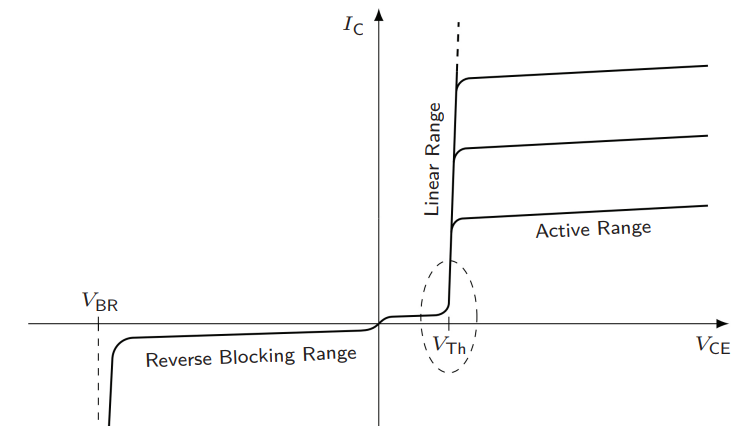
Safet Operating Area (SOA)
IGBTs can be operated at way higher voltages and currents and therefore at hgigher powers than MOSFETs
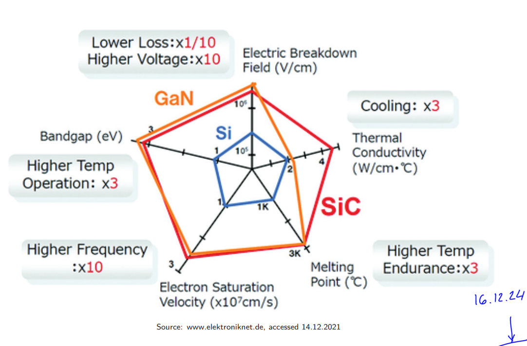
What are modern semiconductor materials?
Bandgap semiconductors (semiconductors with very wide band gap)
SiC or GaN (Gallium Nitride)
Properties and Applications of SiC
High critical field strength → Work at high voltages
High electron mobility (not as high as GaN) → Work at high switching frequencies
High thermal conductivity (highest) → Work with high power density
Useful for SiC Photodiodes (UV-sensitive) and SiC MOSFETs (low on-resistance, smaller cooling surfaces, lower switching times for high precision)
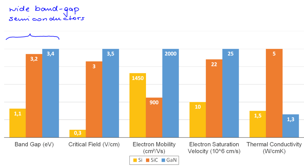
Properties and Applications of GaN
High critical field strength
Very high electron mobility → Work at very high switching frequencies
Low(er) thermal conductivity (work with lower power density)
Used in GaN-HEMT (High Electron Mobility Transfer) fvor high-frequency applications due to low gate capacitance (smaller passive components)
48 V DC/DC converter: 5G infrastructure, AI applicationsm and LIDAR technologies due to stable power supply, high power density and switching frequencies at low cost