scanning tunnelling microscopy (STM)- revision
1/13
There's no tags or description
Looks like no tags are added yet.
Name | Mastery | Learn | Test | Matching | Spaced | Call with Kai |
|---|
No analytics yet
Send a link to your students to track their progress
14 Terms
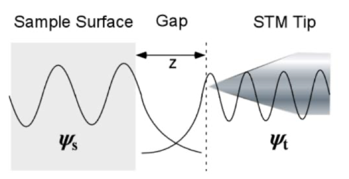
1.The diagram below shows the electron tunnelling process between a tip and the sample in STM.
a. In the diagram what does the symbol Ψ represent?
b. What is electron tunnelling? Why does it occur.
c. How important is z?
a. What does the symbol Ψ represent?
The symbol Ψ (psi) represents the quantum mechanical wavefunction of the electrons:
Ψₛ is the wavefunction of the electrons in the sample surface.
Ψₜ is the wavefunction of the electrons in the STM tip.
The wavefunction describes the probability amplitude of finding an electron in a particular region. Where these wavefunctions overlap (in the gap), electron tunnelling can occur.
b. What is electron tunnelling? Why does it occur?
Electron tunnelling is a quantum mechanical phenomenon where electrons move through a potential energy barrierthat, classically, they don’t have enough energy to overcome.
In STM:
A small bias voltage is applied between the conductive tip and the conductive sample.
When the tip is extremely close to the surface (a few angstroms), their wavefunctions overlap.
Electrons can "tunnel" through the vacuum gap between tip and sample, creating a measurable tunnelling current.
This occurs because in quantum mechanics, there is a non-zero probability of finding an electron in the barrier region (the vacuum), even if its energy is lower than the barrier height.
c. How important is z (the gap distance)?
z is critically important because the tunnelling current is exponentially sensitive to the gap distance:
This means:
A 0.1 nm change in z can change the tunnelling current by an order of magnitude.
STM achieves atomic resolution by measuring these ultra-sensitive changes in tunnelling current as the tip scans the surface.
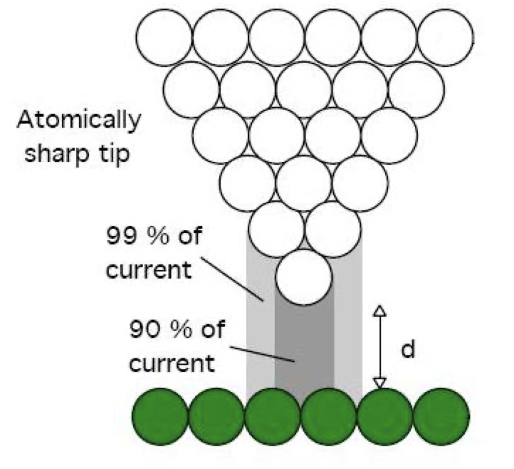
2. The diagram below shows an STM tip near a sample:
a.There is one component missing in the diagram above. Hint – it helps electrons move in one direction.
b. Give the range of values for d.
c. What happens when d = 0?
d. Why is atomic resolution possible in STM?
a. What component is missing from the diagram?
The missing component is the bias voltage source (power supply).
This is essential in STM because it creates a potential difference between the tip and the sample, allowing electron tunnelling in one direction (from tip to sample or vice versa).
Without this voltage, no tunnelling current would flow.
b. What is the range of values for d (tip–sample distance)?
The typical range of d (gap distance) in STM is:
0.3 to 1 nanometre (nm)
This is equivalent to 3–10 angstroms (Å)
At this ultra-short distance, quantum tunnelling becomes possible, but the tip is still physically separated from the sample.
c. What happens when d = 0?
When d = 0, the STM tip touches or contacts the sample.
This results in a mechanical contact rather than a tunnelling interaction.
The tunnelling regime breaks down, and the system may switch to conductive atomic force microscopy (C-AFM) behaviour or cause sample/tip damage.
This is not ideal and typically avoided in STM operation.
next question
Why is W a preferred material or STM tips.
Tungsten (W) is a preferred material for STM (Scanning Tunnelling Microscopy) tips due to its excellent physical, chemical, and electrical properties that make it ideal for high-resolution, stable scanning.
Tungsten’s combination of conductivity, hardness, thermal stability, and ease of sharpening makes it a top choice for crafting reliable, high-resolution STM tips.

When using STM, the feedback control is essential. Why?
Feedback control in Scanning Tunnelling Microscopy (STM) is essential because it ensures stable imaging, maintains constant tunnelling conditions, and enables high-resolution topographic mapping at the atomic scale.
Why Feedback Control Is Essential in STM:
Function | Explanation |
|---|---|
Maintains Constant Tunnelling Current | The tunnelling current depends exponentially on tip–sample distance. Feedback adjusts the vertical position (z) of the tip to keep the current constant. |
Accurate Surface Topography | The z-movement of the tip (controlled by feedback) is recorded as the image. Without it, the topographic data would be inaccurate or blurred. |
Prevents Tip–Sample Contact | If the tip gets too close, it can crash into the sample, causing damage. Feedback rapidly adjusts the tip to prevent this. |
Compensates for Surface Variations | As the tip scans across a surface with atomic bumps and valleys, the feedback loop dynamically adjusts height in real time. |
Enables Stable Imaging | It corrects for drift, vibrations, or noise that could otherwise destabilise tunnelling. |
Feedback control is the core mechanism that allows STM to maintain the tiny, precise distance (a few angstroms) between the tip and surface, enabling atomic-resolution imaging while protecting both the tip and the sample.
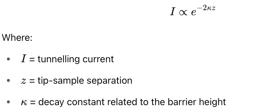
State the equation relating the current and d. Define all the terms in the equation. How big are
electrical currents in STM.
Equation Relating Tunnelling Current and Distance dd in STM
The tunnelling current II in Scanning Tunnelling Microscopy is given by the exponential relationship:
Typical tunnelling currents in STM are extremely small:
Range:
10 pA to 10 nA10 pA to 10 nA
(picamperes to nanoamperes)
These low currents are stable and measurable with sensitive electronics, and they allow non-destructive imaging with atomic-scale precision.
Because the current depends exponentially on distance, even a 0.1 nm change in dd can result in a 10× change in tunnelling current, which is why precise feedback control is so critical in STM.

How important are environmental conditions when operating and STM? Discuss.
Environmental conditions are critically important when operating a Scanning Tunnelling Microscope (STM) because STM relies on measuring extremely small tunnelling currents (in the pA–nA range) and maintaining sub-nanometre tip–sample distances. Even minute external disturbances can affect image quality, resolution, and instrument stability.
1. Vibration Isolation
Why it matters: Even slight vibrations (from footsteps, traffic, or building movement) can cause the STM tip to jump or drift, disrupting the tunnelling condition.
Control: STMs are often mounted on vibration isolation tables or suspended with air-damped platforms to suppress mechanical noise.
Effect: Poor vibration isolation can blur atomic resolution images or prevent proper feedback control.
2. Temperature Stability
Why it matters: Temperature fluctuations cause thermal drift in the sample and the piezoelectric scanner, shifting the tip position during scanning.
Control: STMs are placed in thermally insulated enclosures or operated in temperature-controlled rooms.
Effect: Thermal instability leads to distortion in images, especially in long scans or atomic-resolution work.
3. Acoustic and Electromagnetic Noise
Why it matters: Airborne sound waves and electromagnetic interference (EMI) can introduce noise into the current signal.
Control: STMs are often housed in acoustically shielded and electromagnetically grounded enclosures.
Effect: High noise can mask weak tunnelling currents and reduce signal-to-noise ratio.
4. Vacuum or Atmospheric Control
Why it matters: Many STMs operate in ultra-high vacuum (UHV) to prevent contamination and oxidation, especially when using reactive tip materials like tungsten.
Alternative: Some STMs work in ambient air or in liquids for biological or electrochemical samples, but resolution is usually reduced.
Effect: Poor vacuum can alter tip shape, contaminate surfaces, or introduce drift due to outgassing.
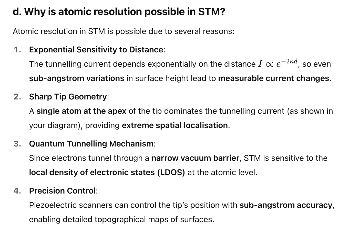
The STM image of graphene on carbon is shown below.
The imaging was taken with a scan speed of 2Hz with resolution 256 x 256 pixels. Calculation the
time taken to collect the image

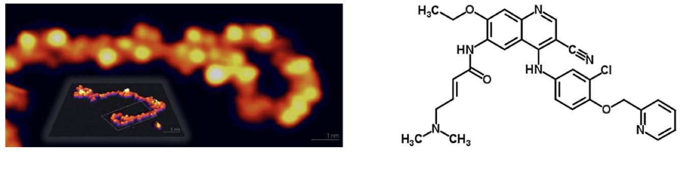
8. The STM image of unfolded BSA is shown below:
a. Comment on what you can see.
b. Explain the main difficulties in obtaining such an image.
c. How could you improve the resolution of the STM image.
a. Comment on what you can see.
The STM image shows a chain-like structure consistent with an unfolded protein molecule (BSA), displayed with nanometre resolution. The molecule appears as a bright, irregular path, likely reflecting regions of varying height and electron density. The colour contrast represents topographical features, and the inset 3D view highlights the overall curvature and conformation of the protein on the substrate. At this scale (~1–5 nm), individual subdomains or amino acid chains may be partially resolved, although atomic resolution is not fully achieved
b. Explain the main difficulties in obtaining such an image.
Protein Instability and Motion:
Proteins like BSA are soft and flexible. They can move, collapse, or denature when placed on a surface, especially under vacuum or without proper fixation.Sample Preparation:
Unfolded proteins must be adsorbed onto a conductive substrate without aggregation or conformational collapse. This is chemically and technically demanding.Non-conductivity of Biomolecules:
BSA is non-conductive, so tunnelling current is weak. Imaging often requires modified tips, functionalisation, or ultra-high vacuum (UHV) to enhance contrast.STM Tip Stability:
Maintaining an atomically sharp tip and controlling drift, vibrations, and noise is critical. Imaging such a soft, extended molecule requires a highly stable system.Resolution Limits:
The large molecular size, combined with thermal vibrations and surface interactions, limits atomic-level resolution.
c. How could you improve the resolution of the STM image?
Use of UHV Conditions:
Reduces contamination, stabilises the molecule, and improves signal-to-noise ratio.Cryogenic Temperatures:
Cooling the sample to liquid helium or nitrogen temperatures reduces molecular motion and thermal drift.Functionalised Tips:
Coating the STM tip with specific molecules (e.g., CO-terminated tips) can enhance resolution and interaction sensitivity.Optimised Sample Preparation:
Use atomically flat, conductive substrates (e.g., Au(111), HOPG) and gentle deposition techniques to preserve native conformation.Signal Filtering and Slow Scanning:
Slower scan speeds and signal averaging reduce noise, while feedback optimisation improves vertical sensitivity.
what are the limitations of STM?
Scanning Tunnelling Microscopy (STM) is a powerful technique capable of imaging surfaces at atomic resolution, but it has several important limitations that affect its applicability and performance:
1. Requires Conductive or Semiconductive Samples
Limitation: STM relies on electron tunnelling, so the sample must conduct electricity.
Impact: Insulators and most biological samples (e.g., DNA, proteins) cannot be imaged directly without modification or special techniques (e.g., coating, conductive substrate).
2. Limited to Surface Imaging
Limitation: STM only maps the topmost atomic layers.
Impact: It cannot provide subsurface or bulk structural information, unlike techniques such as TEM or AFM (in tapping mode).
3. Ultra-Clean and Stable Environment Needed
Limitation: STM is highly sensitive to vibrations, temperature drift, and contamination.
Impact: Requires ultra-high vacuum (UHV), vibration isolation, and often low temperatures for stable, high-resolution imaging.
4. Difficult Sample Preparation
Limitation: Samples must be atomically flat, clean, and well-prepared on conductive substrates.
Impact: Limits the range of materials that can be studied easily, especially complex or rough samples.
5. Slow Imaging Speed
Limitation: Scanning is line-by-line, with feedback adjustments per point.
Impact: High-resolution imaging can take minutes to hours, limiting throughput and live imaging capability.
6. Tip Condition Affects Results
Limitation: Imaging depends on the quality and shape of the STM tip.
Impact: Contamination or blunting of the tip can distort images, cause artefacts, or reduce resolution.
7. No True Chemical Information
Limitation: STM primarily measures electronic density of states and topography.
Impact: Cannot directly identify atomic species (though combined STM/STS or functionalised tips can offer limited chemical sensitivity)
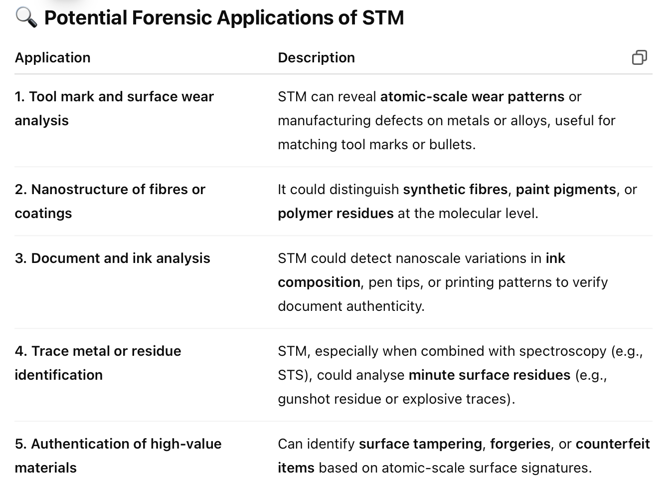
10. Do you see any potential use of STM for forensic science.
Yes, Scanning Tunnelling Microscopy (STM) holds promising potential for forensic science, particularly in nano-scale surface analysis and trace evidence examination, though its use is currently limited by practical constraints. Here's how STM could contribute:
Current Limitations in Forensic Use
Non-conductive materials (e.g., many biological and organic forensic samples) are difficult to image.
Sample prep is demanding and often destructive.
Requires ultra-high vacuum (UHV) and stable lab conditions, not field-operable.
High cost and need for specialised operators.